Scanning Tunneling Spectroscopy of Suspended Single-Wall Carbon Nanotubes
Abstract
We have performed low-temperature STM measurements on single-wall carbon nanotubes that are freely suspended over a trench. The nanotubes were grown by CVD on a Pt substrate with predefined trenches etched into it. Atomic resolution was obtained on the freestanding portions of the nanotubes. Spatially resolved spectroscopy on the suspended portion of both metallic and semiconducting nanotubes was also achieved, showing a Coulomb-staircase behavior superimposed on the local density of states. The spacing of the Coulomb blockade peaks changed with tip position reflecting a changing tip-tube capacitance.
Transport measurements on single-wall carbon nanotubes (SWCNTs) show Coulomb blockade Bockrath et al. (1997); Tans et al. (1997) and Luttinger liquid behavior.Bockrath et al. (1999); Yao et al. (1999) While it would be desirable to use the high spatial resolution of scanning tunneling microscopy (STM) to study these effects, they are obscured by the close proximity of a conducting substrate. Suspending SWCNTs can circumvent this limitation. Several ways of suspending SWCNTs for transport measurements have been reportedTombler et al. (2000); Nygard and Cobden (2001) but none of these is compatible with STM.
In this letter, we demonstrate that it is possible to obtain atomic-resolution STM images and perform local spectroscopy measurements on suspended carbon nanotubes. The tubes are grown across trenches on a metallic substrate to allow STM imaging. Spatially resolved spectroscopy on metallic and semiconducting nanotubes shows a Coulomb staircase due to the addition of single electrons. The spacing between steps in the staircase corresponds to the energy necessary to add an electron. By measuring this spacing, we determine the capacitance between the tip and nanotube, which is found to depend on the distance of the tip from the edge of the trench.
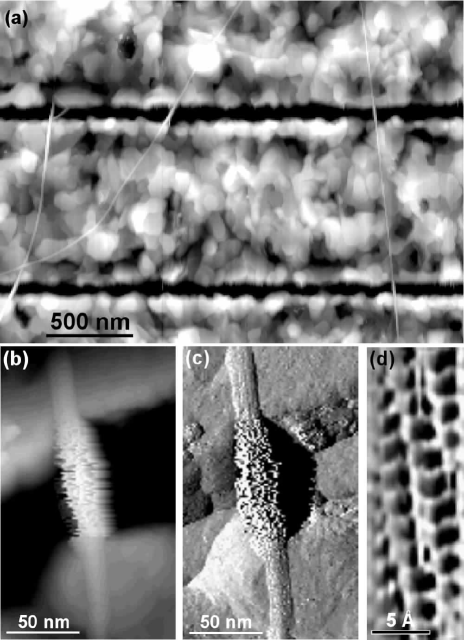
Figure 1(a) shows an Atomic Force Microscopy (AFM) image of the structure with suspended carbon nanotubes. 100 nm wide trenches were dry-etched in SiO2 to a depth of 200 nm. The spacing between trenches was 1 m. After the etching, a 100 nm thick film of Pt was deposited onto the entire sample by evaporation to create a conducting substrate. This was followed by deposition of 5 m square areas of Fe:Mo catalyst. Nanotubes were grown from the catalyst by CVD at 800 ∘C for ten minutes.Kong et al. (1998) The tubes grow from the catalyst in random directions; some of them cross over the trenches and are therefore suspended for a distance of approximately 100 nm. The nanotubes can be seen as narrow straight lines running over the trenches in several locations of Fig. 1(a).

The samples were measured using a UHV low-temperature STM with a base temperature of 4.7 K (Omicron LT-STM). STM tips were mechanically cut from Pt-Ir wire. The tips are sufficiently blunt ( 60 nm radius of curvature) that the apex never reaches the bottom of the trench. Figure 1(b) is a STM topography image in constant current mode of a nanotube crossing a trench. The dark horizontal area is the trench, which the nanotube crosses. Figure 1(c) shows the corresponding current image. The nanotube appears slightly higher in the region over the trench due to attractive forces between the tip and nanotube. This attraction also leads to sharp spikes in the current because of the movement of the nanotube. The dark area (no current) to the right of the nanotube is where the tip loses contact with the tube and where it has not yet reached the trench.
Figure 1(d) is an image showing atomic resolution on the free-standing portion of the nanotube. The height of the atoms measured in constant current mode was approximately 4 Å. This is about five times larger than on supported nanotubes. The large apparent height of the atoms may be due to the ability of the nanotube to move due to the forces acting on it from the tip. These images demonstrate the ability to image and obtain atomic resolution on free-standing nanotubes.
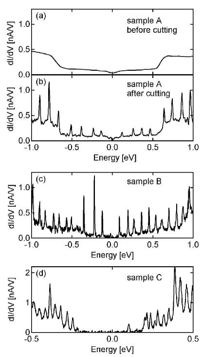
Figure 2(a) shows spectroscopy on a suspended nanotube. The spectroscopy curves were obtained using lock-in detection (867 Hz). We observe a constant density of states at low energy and the first van Hove singularities are visible at higher energies, characteristic of a metallic nanotube.Wildoer et al. (1998); Odom et al. (1998) The nanotube was then cut to a shorter length by applying voltage pulses to it on both sides of the trench, reducing its length to 140 nm.Venema et al. (1997) Figure 2(b) plots the differential conductance after cutting. Sharp spikes have appeared superimposed on the background density of states. The spike pattern can be attributed to Coulomb blockade, where the peaks are caused by the addition of single electrons to the SWCNT.

The Coulomb staircase is characterized by the resistances and capacitances of the two tunnel barriers. These determine the slope of the curve and also the spacing between peaks in . The resistances and capacitances in the system can be determined from the spectroscopy measurements.Grabert and Devoret (1992); Hanna and Tinkham (1991) The tunneling gap between the tip and the SWCNT ensures that , where is the resistance between the tip and the SWCNT and is between the SWCNT and substrate. Therefore, approximately equals the total resistance as determined by the tunneling setpoint. The capacitance between the tip and the SWCNT, is determined from the spacing between peaks in the Coulomb staircase,
| (1) |
Here we have neglected the level spacing in the SWCNT, which causes a small variation in the values of as discussed below. The capacitance between the SWCNT and the substrate, is determined from the slope between steps in the curves. For the nanotube of Fig. 2 (b), 1 aF and 10 aF. The value for is in agreement with numerical simulations, where the tip is modelled as a 60 nm radius sphere. A rough estimate for the capacitance of a cylinder lying above a metal plane gives a value of 0.06 aF/nm, or 2.4 aF for our nanotube, consistent with the observed order of magnitude. We have observed that reducing the tunnel current increases the peak spacing. This is consistent with the increased distance between tip and SWCNT decreasing . We have also observed that the height of the spikes in is proportional to the density of states; the peaks increase in height at energies greater than the first van Hove singularities. This is also consistent with the Coulomb staircase model.
Figure 2(c) shows spectroscopy on another metallic nanotube. In this case a Coulomb staircase was observed without cutting the nanotube. This is the behavior that is seen more often in our nanotubes; we have observed the Coulomb staircase on all 12 SWCNTs that we have measured, with 9 showing it without being cut. It is attributed to the presence of local defects (tunnel barriers) induced by the edges of the trench. These may be caused by the nanotube bending at the edge of the trench, therefore creating a tunnel barrier. When the tunnel barriers are present, the relevant length for the nanotube device is approximately the distance between the two metal contacts. Once again, we can determine the capacitances from the spectroscopy data. The measured capacitances were 2 aF and 1 aF. The low value for further supports the conclusion that there is a tunnel barrier near the edge of the trench, isolating the portion of the nanotube that is over the trench from the part that is on the Pt.
Figure 2(d) shows spectroscopy on a suspended semiconducting nanotube. At low energy, there is a gap while at higher energy there is a finite density of states. Once the energy is sufficient to overcome the gap, the spikes from the Coulomb staircase appear superimposed on the local density of states. This shows that the Coulomb staircase is not particular to the metallic nanotubes but rather is a generic feature of suspended nanotubes.

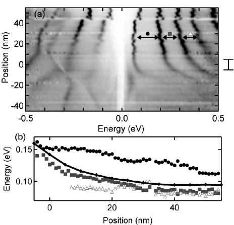
We have also performed spatially resolved spectroscopy on nanotubes going over a trench. Figure 3(a) plots the local density of states as a function of position in a metallic nanotube. Our best estimate for the position of the edge of the trench from topography measurements is indicated by the bracket on the right of the image. The dark lines correspond to high conductance and the addition of electrons. The spacing between peaks in the Coulomb staircase, , is determined by the capacitance between the tip and the nanotube (Eq. 1). The increased spacing of the Coulomb peaks as the tip approaches the edge of the trench implies that the capacitance is decreasing. This is due to screening of the field from the tip by the metal of the substrate. The spacing between successive peaks thus gives a local measurement of the capacitance between the tip and nanotube. We observed no change in along the length of the nanotube.
Figure 3(b) shows the energy spacing between the Coulomb peaks as a function of position along the nanotube. We have performed a numerical simulation of the capacitance between the tip and nanotube. The calculated capacitances have been converted to a peak spacing using Eq. 1. The solid line plots the result showing qualitative agreement with the measured peak spacing. The simulations predict a 30% decrease in the capacitance when the tip is at the edge of the trench compared to the center.
We attribute the different spacings between peaks to the level spacing in the nanotube. The average spacing between levels in a nanotube is given by where is the Fermi velocity and is Planck’s constant. For a 100 nm nanotube, is 9 meV. The measured energy difference between peaks must be scaled by the fraction of the voltage that drops across the tip-nanotube junction, . This is a factor of 1/3 for the nanotube of Fig. 3(b), giving a of 12 meV in good agreement with the expected for a 100 nm nanotube.
We have demonstrated that it is possible to obtain atomic resolution and perform spectroscopy measurements on suspended individual single-walled carbon nanotubes. The suspended portions of the nanotubes showed a Coulomb staircase, which is not observed in conventional STM measurements due to the large . The Coulomb staircase allows a local determination of the capacitance between the tip and nanotube. The ability to fabricate and image devices with freely suspended nanotubes will allow simultaneous transport and scanning tunneling spectroscopy measurements.
The authors would like to thank NWO Pionier and FOM for funding, and Abdou Hassanien who was involved in earlier stages of this project.
References
- Bockrath et al. (1997) M. Bockrath et al., Science 275, 1922 (1997).
- Tans et al. (1997) S. Tans et al., Nature 386, 474 (1997).
- Bockrath et al. (1999) M. Bockrath et al., Nature 397, 598 (1999).
- Yao et al. (1999) Z. Yao et al., Nature 402, 273 (1999).
- Tombler et al. (2000) T. Tombler et al., Nature 405, 769 (2000).
- Nygard and Cobden (2001) J. Nygard and D. H. Cobden, Appl. Phys. Lett. 79, 4216 (2001).
- Kong et al. (1998) J. Kong et al., Nature 395, 6705 (1998).
- Wildoer et al. (1998) J. W. G. Wildoer et al., Nature 391, 59 (1998).
- Odom et al. (1998) T. W. Odom et al., Nature 391, 62 (1998).
- Venema et al. (1997) L. Venema et al., Appl. Phys. Lett. 71, 2629 (1997).
- Grabert and Devoret (1992) H. Grabert and M. H. Devoret, Single Charge Tunneling (Plenum, New York, 1992).
- Hanna and Tinkham (1991) A. E. Hanna and M. Tinkham, Phys. Rev. B 44, 5519 (1991).