Ab-initio study of the electric transport in gold nanocontacts
Abstract
By employing a real-space formulation of the Kubo-Greenwood equation based on a Green’s function embedding technique combined with the fully relativistic spin-polarized Korringa-Kohn-Rostoker method a detailed investigation of the electrical transport through atomic-scaled contacts between two Au(001) semi-infinite systems is presented. Following a careful numerical test of the method the conductance of Au nanocontacts with different geometries is calculated. In particular, for a contact formed by a linear chain of Au atoms a conductance near 1 is obtained. The influence of transition metal impurities (Pd, Fe and Co) placed on various positions near the center of a particular contact is also studied. We found that the conductance is very sensitive to the position of the magnetic impurities and that the mechanism for the occurring relative changes can mainly be attributed to the impurities’ minority -band inducing resonant line-shapes in the -like DOS at the center of the contact.
pacs:
73.20.Hb, 73.63.Rt, 73.40.Jn, 75.75.+aI Introduction
The number of theoretical and experimental investigations of electronic structure and transport properties of atomic-sized conductors has greatly been increased over the last decade. The increasing interest for investigating atomic-sized conductors is driven by the possibility of using such systems in future nanoelectronic technologies. Widely applied methods for fabricating nanocontacts between macroscopic electrodes are the mechanically controllable break junction (MCBJ) technique mcbj1 ; mcbj2 ; Smit ; halbritter and scanning tunneling microscopy (STM) crommie ; gimzewski ; brandbyge by pushing the tip intentionally into the surface. The crucial problems for both methods are the presence of contaminants and the mechanical stability. At sufficiently low temperatures the measurements revealed a quantized conductance for atomic sized nanocontacts made of various materials, not only pure metals but also alloys AuPd ; heemskerk . Nanocontacts made of gold are presumably the most studied systems in the literature both theoretically and experimentally. A dominant peak very close to the conductance quantum, 1 , has been reported for gold (and other noble metals) in the conductance histogram mcbj2 ; brandbyge , attributed to the highly transmitting –channel across a linear chain connecting the two electrodes. It was also found that the chain formation is in close connection with surface reconstruction phenomena Smit . For a comprehensive review of the field of atomic-sized conductors, see Ref. RuitRev, .
In order to understand the mechanism of nanocontact formation, electronic structure and transport, different theoretical methods have been developed. Some theoretical studies use tight–binding methods brandbyge1 ; solanki , others are based on ab initio density functional theory stepanyuk ; mertig ; opitz . Most of the transport studies rely on the Landauer-Büttiker approach landauer ; buttiker , although Baranger and Stone adopted the more sophisticated Kubo-Greenwood formula kubo ; greenwood ; luttinger ; butler for calculating the conductance between free electron leads baranger . By using this approach a recent study mertig focused on the effect of transition metal imperfections inserted into an infinite Cu wire showing that the conductance of the wire decreased due to the different conductance for the two spin channels (spin-filter effect).
The fully relativistic screened Korringa-Kohn-Rostoker (SKKR) Green’s function method proved to be an effective method to calculate electronic structure and magnetic properties of layered systems skkr ; rsp-skkr . Combined with an embedding technique based on multiple scattering theory, calculations have been performed for magnetic clusters on surfaces bence1 ; bence2 ; bence3 . Employing the Kubo-Greenwood formula within this method permits one to investigate transport properties of atomic sized structures palotas . In this paper we report on calculations of transport properties of gold nanocontacts. We first briefly review the theoretical background of the applied method and give numerical evidence of its reliability. We then calculate and analyze the conductance for different atomic arrangements between semi-infinite Au(001) systems and investigate the effect of transition metal impurities on the conductance. We find a qualitatively satisfactory explanation of the observed changes in the conductance in terms of changes in the -like local density of states (LDOS) at the center of the point contact caused by interactions with the -like states of the impurity.
II Theoretical approach
II.1 Expression of the conductivity
The static limit of the optical conductivity tensor is given by the Kubo-Luttinger formula kubo ; luttinger as
| (1) | ||||
where V is the volume of the system, is the Fermi-Dirac distribution function, is the th component ( or ) of the current density operator, are the corresponding (upper or lower) side limits of the resolvent of an appropriate Kohn-Sham(-Dirac) Hamiltonian, while denotes the trace of an operator. Integration by parts yields
| (2) |
with
| (3) |
which has the meaning of a zero-temperature, energy dependent conductivity. For is obviously given by
| (4) |
A numerically tractable formula can be obtained only for the diagonal elements of the conductivity tensor, namely,
| (5) |
yielding the widely used Kubo-Greenwood formula greenwood ; butler of the dc-conductivity at finite temperatures,
| (6) |
On the other hand, Eq. (1) can be reformulated as follows,
| (7) | ||||
namely in terms of an equation which is similar to the formulation of Baranger and Stone baranger but clearly can be cast into a relativistic form.
II.2 Expression of the conductance
Linear response theory applies to an arbitrary choice for the perturbating electric field because the response function is obtained in the zero limit of perturbation. Let us assume, therefore, that a constant electric field, , pointing along the axis, i.e., normal to the planes, is applied in all cells of layer . Denoting the component of current density averaged over cell in layer by , the microscopic Ohm’s law reads as
| (8) |
where is the volume of the unit cell in layer . Note, that in neglecting lattice relaxations, is uniform in the whole system. According to the Kubo-Greenwood formula, Eq. (6), the component of the non-local conductivity tensor, can be written at zero temperature as
| (9) | ||||
Here the integration is carried out over the th unit cell in layer , , and the th unit cell in layer , , while denotes a trace over four-component spinors. The total current flowing through layer can be written as
| (10) |
where the applied voltage is
| (11) |
and and denote the area of the 2D unit cell and the interlayer spacing, respectively (). Combining Eqs. (8),(10) and (11) results in an expression for the conductance,
| (12) |
where the summations should, in principle, be carried out over all the cells in layers and . An alternative choice of the non-local conductivity tensor is given by Eq. (II.1). This leads to a huge simplification for the conductance because, as shown by Baranger and Stone baranger for free electron leads, the second term appearing in Eq. (II.1) becomes identically zero when integrated over the layers, . It should be noted that recently Mavropoulos et al. mavropoulos rederived this result by assuming Bloch boundary conditions for the leads. The conductance can thus be written as
| (13) |
It has to be emphasized that because of the use of linear response theory and current conservation, the choice of layers and is arbitrary in the above formula. The numerical test of the method will clearly demonstrate this feature (see Section III.). On the other hand, as shown in Ref. mavropoulos, , when the layers and are asymptotically far from each other, the present formalism naturally recovers the Landauer-Büttiker approach landauer ; buttiker .
II.3 Computational details
Using the embedding technique of multiple scattering the matrix representation of the scattering path operator (SPO) of a given cluster, , with and denoting sites in the cluster, and indexing angular momentum quantum numbers, can be expressed as bence1
| (14) |
where , stand for the corresponding single-site t-matrices of the host medium and the cluster, and for the host-SPO. For a two-dimensional (2D) translational invariant host medium, the latter one is calculated by
| (15) |
where and are 2D lattice vectors and the integral is performed over the 2D Brillouin zone of area .
The self-consistent calculations for both the host and the finite clusters were performed within the local spin-density approximation (LSDA) Vosko , by using the atomic sphere approximation (ASA) and for the angular momentum expansion. The semi-infinite host system was evaluated in terms of the screened Korringa-Kohn-Rostoker method (SKKR) skkr ; rsp-skkr by sampling 45 points in the irreducible (1/8) part of the fcc(001) Brillouin zone, see Eq. (15), and 16 energy points along a semi-circular contour in the upper complex energy semi-plane. The latter set-up also applied for the self-consistent cluster calculations, whereby a sufficiently large number of atoms from the neighboring host (including sites in the vacuum) was taken into account in order to serve as a buffer for charge fluctuations. In the case of magnetic impurities, the orientation of magnetization was chosen to be normal to the fcc(001) planes (direction ). Additional calculations of the magnetic anisotropy energy confirmed this choice.
In terms of the SPO the conductance in Eq. (13) can be calculated as
| (16) |
where stands for the relativistic angular momentum representation of the current density operator in cell of layer (see, e.g., in Ref. palotas, ), and, correspondingly, the trace is performed in angular momentum space. Inherent to the SKKR method, a finite imaginary part, , of the Fermi energy has to be applied, , which, however, has to be continued to zero in order to ensure current conservation. Concomitantly, the number of points taken in Eq. (15) has to be considerably increased. All results presented in the next Section for the conductance refer to Ryd.
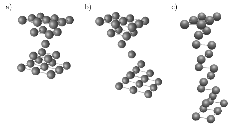
In the present work no geometry optimization has been carried out, that means all of the considered sites (both Au, vacuum and impurity sites) correspond to the positions of an ideal fcc(001) structure of gold with a lattice constant of A schematic view of a typical contact is displayed in Fig. 1. As follows from the above, atomic sites refer to layers for which we use the notation: the central layer, and the layers below and above, etc. For the contact shown in Fig. 2a, e.g., the central layer contains 1 Au atom (the rest is built up from empty spheres), layers and contain 4 Au atoms, layers and contain 9 Au atoms and, though not shown, all layers and () are completely filled with Au atoms and will be denoted by full layers.
III Results and discussion
III.1 Numerical tests on different gold contacts
As mentioned in Section II a finite Fermi level broadening, , has to be used for the conductance calculations. As an example, for the point contact depicted in Fig. 2a, we investigated the dependence of the conductance on . The summation in Eq. (16) was carried out up to convergence for the first two (symmetric) full layers (). As can be seen from Fig. 3, the calculated conductances depend strongly but nearly linear on . A straight line fitted for mRyd intersects the vertical axis at 2.38 . Assuringly enough, a calculation with Ryd resulted in . Although the nearly linear dependence of the conductance with respect to enables an easy extrapolation to , as what follows all the calculations refer to Ryd.
For the same type of contact we investigated the convergence of the summation in Eq. (16) over the layers and , whereby we chose different symmetric pairs of full layers. The convergence with respect to the number of atoms in the layers is shown in Fig. 4. Convergence for about 20 atoms can be obtained for the first two full layers (), whereas the number of sites needed to get convergent sums gradually increases if one takes layers farther away from the center of the contact. This kind of convergence property is qualitatively understandable since the current flows from the contact within a cone of some opening angle that cuts out sheets of increasing area from the corresponding layers. As all the calculations were performed with Ryd, current conservation has to be expected. Consequently the calculated conductance ought to be independent with respect to the layers chosen for the summation in Eq. (16). As can be seen from Fig. 4 this is satisfied within a relative error of less then 10%. It should be noted, however, that for the pairs of layers, , convergence was not achieved within this accuracy: by taking more sites in the summations even a better coincidence of the calculated conductance values for different pairs of layers can be expected. Fig. 4 also implies that an application of the Landauer-Büttiker approach to calculate the conductance of nanocontacts is numerically more tedious than the present one, since, in principle, two layers situated infinitely far from each other have to be taken in order to represent the leads.
Although only one Au atom is placed in the center of the point contact considered above, see Fig. 2a, the calculated conductance is more than twice as large as the conductance unit. This is easy to understand since the planes and , each containing four Au atoms, are relatively close to each other and, therefore, tunneling contributes quite a lot to the conductance through the contact. In order to obtain a conductance around 1 , detected in the experiments, a linear chain has to be considered. The existence of such linear chains is obvious from the long plateau of the corresponding conductance trace with respect to the piezo voltage in the break-junction experiments. Since, as mentioned in Section II, our method at present can only handle geometrical structures confined to three dimensional translational invariant simple bulk parent lattices, as the simplest model of such a contact we considered a slanted linear chain as shown in Fig. 2b. In here, the middle layer () and the adjacent layers () contain only one Au atom, layers and 4 and 9 Au atoms, respectively, while layers refer to the first two full layers. The sum in Eq. (16) was carried out for two pairs of layers, namely for , (full layers) and for , (not full layers). The convergence with respect to the number of atoms in the chosen layers can be seen from Fig. 5. The respective converged values are 1.10 and 1.17 . In the case of , we observed that the contribution coming from the vacuum sites is nearly zero: considering only 4 Au atoms in the summation already gave a value for the conductance close to the converged one. The small difference between the two calculated values, 0.07 , can most likely be attributed to an error caused by the ASA. Nevertheless, as expected, the calculated conductance is very near to the ideal value of 1 .
Another interesting structure is the 2x2 chain described in Ref. mertig, . Here we considered a finite length of this structure sandwiched between two semi-infinite systems, see Fig. 2c. The conductance was calculated by performing the summation for 100 atoms from each of the first two full layers. As a result we obtained a conductance of 2.58 . Papanikolaou et al. mertig got a conductance of 3 for an infinite Cu wire to be associated with three conducting channels within the Landauer approach. For an infinite wire the transmission probability is unity for all states, therefore, the conductance is just the number of bands crossing the Fermi level. For the present case of a finite chain, the transmission probability is less than unity for all the conducting states. This qualitatively explains the reduced conductance with respect to an infinite wire.
Finally, we studied the dependence of the conductance on the thickness of the nanocontacts. All the investigated structures have symmetry and the central layer of the systems is a plane of reflection symmetry. The set-up of the structures is summarized in Table 1. Contact 0 refers to a broken contact, while the others have different thicknesses from 1 up to 9 Au atoms in the central layer. In Fig. 6 the calculated conductances are displayed as performed by taking nearly 100 atoms from each of the first two full layers: for the broken contact and for all the other cases, see Table 1. It can be seen that the conductance is nearly proportional to the number of Au atoms in the central layer. This finding can qualitatively be compared with the result of model calculations for the conductance of a three-dimensional electron gas through a connective neck as a function of its area in the limit of for the opening angle Torres . In the case of the broken contact, the non-zero conductance can again be attributed to tunneling of electrons.
III.2 Gold contact with an impurity
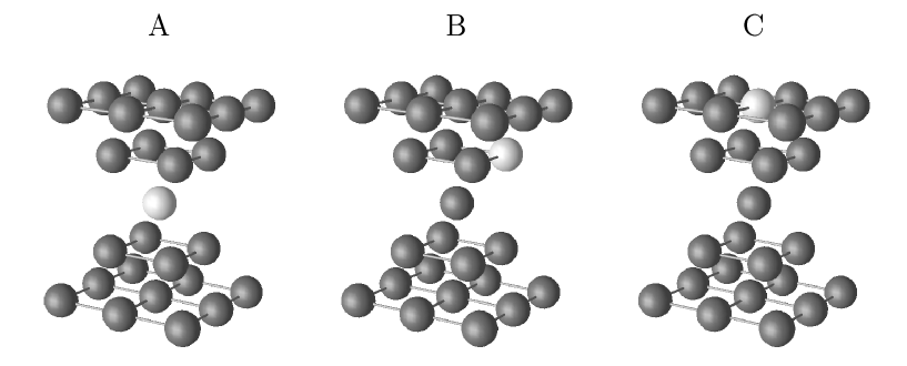
In recent break junction experiments AuPd remarkable changes of the conductance histograms of nanocontacts formed by AuPd alloys have been observed when varying the Pd concentration. Studying the effect of impurities placed into the nanocontact are, in that context, at least relevant for dilute alloys. The interesting question is whether the presence of impurities can be observed in the measured conductance. For that reason we investigated transition metal impurities such as Pd, Fe, and Co placed at various positions of the point contact as shown in Fig. 2a. For the notation of the impurity positions see Fig. 7. The calculated spin and orbital moments of the magnetic impurities are listed in Table 2. As usual for magnetic impurities with reduced coordination numberbence1 , both for Fe and Co we obtained remarkably high spin moments, and in all positions of a Co impurity large orbital moments. In particular, the magnitude of the orbital moments is very sensitive to the position of the impurity. This is most obvious in case of Fe, where at positions B and C the orbital moment is relatively small, but at position A a surprisingly high value of 0.47 was obtained.
The summation over 116 atoms from each of the first two full layers () in Eq. (16) has been carried out in order to evaluate the conductance. The calculated values are summarized in Table 3. A Pd impurity (independent of position) reduces only little the conductance as compared to a pure Au point contact. This qualitatively can be understood from the local density of states (LDOS) of the Pd impurity (calculated by using an imaginary part of the energy of = 1 mRyd). In Fig. 8 we plotted the corresponding LDOS at positions A and C. Clearly, the change of the coordination number (8 at position A and 12 at position C), i.e., different hybridization between the Pd and Au bands, results into different widths for the Pd -like LDOS. In both cases, however, the Pd states are completely filled and no remarkable change in the LDOS at Fermi level (conducting states) happens.
The case of the magnetic impurities seems to be more interesting. As can be inferred from Table 3, impurities at position B change only a little the conductance. Being placed at position A, however, Fe and Co atoms increase the conductance by 11 % and 24 %, while at position C they decrease the conductance by 19 % and 27 %, respectively. In Ref. mertig, it was found that single Fe, Co (and also Ni) defects in a 2x2 infinite Cu wire decreased the conductance. By analyzing the DOS it was concluded that the observed reduction of the conductance is due to a depletion of the states in the minority band. The above situation is very similar to the case of an Fe or Co impurity in position C of the point contact considered, even the calculated drop of the conductance ( -20 % for Fe and -28 % for Co) agrees quantitatively well with our present result. Our result, namely, that Fe and Co impurities at position A increase the conductance can, however, not be related to the results of Ref. mertig, . In order to understand this feature we have to carefully investigate the LDOS calculated for the point contact.
In Fig. 9 we plotted the minority -like LDOS of the Fe and Co impurities in positions A and C as resolved according to the canonical orbitals , , , and . We have to stress that this kind of partial decomposition, usually referred to as the representation of the LDOS, is not unique within a relativistic formalism, since due to the spin-orbit interaction the different spin- and orbital components are mixed. However, due to the large spin-splitting of Fe and Co the mixing of the majority and minority spin-states can be neglected. As can be seen from Fig. 9, the LDOS of an impurity in position A is much narrower than in position C. This is an obvious consequence of the difference in the coordination numbers (8 for position A and 12 for positions C). Thus an impurity in position A hybridizes less with the neighboring Au atoms and, as implied by the LDOS, the corresponding states are fairly localized. Also to be seen is a spin-orbit induced splitting of about 8 mRyd ( 0.1 eV) in the very narrow - states of the impurities in position A. The difference of the band filling for the two kind of impurities shows up in a clear downward shift of the LDOS of Co with respect to that of Fe.
In explaining the change of the conductance through the point contact caused by the impurities in positions A and C, the -like DOS at the center site, i.e., at the narrowest section of the contact, is plotted in the top half of Fig. 10. As a comparison the corresponding very flat -like DOS is shown for a pure Au contact. For contacts with impurities this -like DOS shows a very interesting shape which can indeed be correlated with the corresponding -like DOS at the impurity site, see bottom half of Fig. 10. Clearly, the center positions and the widths of the -like DOS peaks and those of the respective (anti-)resonant -like DOS shapes coincide well with each other. This kind of behavior in the DOS resembles to the case studied by Fano for a continuum band and a discrete energy level in the presence of configuration interaction (hybridization) Fano . Apparently, by keeping this analogy, in the point contact the -like states play the role of a continuum and the -like state of the impurity acts as the discrete energy level. Since the two kinds of states share the same cylindrical symmetry, interactions between them can occur due to backscattering effects. It should be noted that similar resonant line-shapes in the STM I-V characteristics have been observed for Kondo impurities at surfaces madhavan ; manoharan and explained theoretically ujsaghy .
Inspecting Fig. 10, the enhanced -like DOS at the Fermi level at the center of the point contact provides a nice interpretation to the enhancement of the conductance when the Fe and Co impurity is placed at position A. As the peak position of the -like states of Fe is shifted upwards by more than 0.01 Ryd with respect to that of Co, the corresponding resonance of the -like states is also shifted and the -like DOS at the Fermi level is decreased. This is also in agreement with the calculated conductances. In the case of impurities at position C, i.e., in a position by = 7.63 a.u. away from the center of the contact, the resonant line-shape of the -like states is reversed in sign, therefore, we observe a decreased -like DOS at the Fermi level, explaining in this case the decreased conductance, see Table 3. Since, however, the -like DOS for the case of a Co impurity is larger than for an Fe impurity, this simple picture cannot account correctly for the opposite relationship we obtained for the corresponding conductances.
Summary
By using a Green’s function technique based on the embedding scheme of the multiple scattering theory and the Kubo-Greenwood linear response theory as formulated by Baranger and Stone baranger we studied the conductance of gold nanocontacts depending on the contact geometry and transition metal impurities placed at various positions. We performed several numerical tests that proved the efficiency of our method. In good agreement with experiments and other calculations we obtained a conductance of 1.1 for a finite linear chain connecting two semi-infinite Au leads. The calculated conductance for a thicker 2x2 wire, 2.58 , can be related to a recent result for an infinite 2x2 chain (3 ) mertig . Also in agreement with quantum mechanical model calculations Torres we found a nearly linear dependence of the conductance on the “thickness” of the contact. By embedding magnetic transition metal impurities into a point contact we found both enhancement and reduction of the conductance depending on the position of the impurities. On analyzing the local density of states we concluded that the effect of the impurity is mainly controlled by the interaction of the minority -like and -like states giving rise to a resonant line-shape (Fano-resonance) in the -like DOS at the center of contact. We suggest that this line-shape should also be observed in conductance characteristics providing thus an “experimental” tool to detect magnetic impurities (even their position) in a noble metal point contact.
Acknowledgements
This paper resulted from a collaboration partially funded by the RTN network “Computational Magnetoelectronics” (Contract No. HPRN-CT-2000-00143) and by the Research and Technological Cooperation Project between Austria and Hungary (Contract No. A-3/03). Financial support was also provided by the Center for Computational Materials Science (Contract No. GZ 45.451), the Austrian Science Foundation (Contract No. W004), and the Hungarian National Scientific Research Foundation (OTKA T038162 and OTKA T037856).
References
- (1) C.J. Muller, J.M. van Ruitenbeek, and L.J. de Jongh, Phys. Rev. Lett. 69, 140 (1992)
- (2) J.M. Krans, I.K. Yanson, Th.C.M. Govaert, R. Hesper, and J.M. van Ruitenbeek, Phys. Rev. B 48, 14721 (1993)
- (3) R.H.M. Smit, C. Untiedt, A.I. Yanson, and J.M. van Ruitenbeek, Phys. Rev. Lett. 87, 266102 (2001)
- (4) A. Halbritter, Sz. Csonka, O. Yu. Kolesnychenko, G. Mihály, O.I. Shklyarevskii, and H. van Kempen, Phys. Rev. B 65, 045413 (2002); Sz. Csonka, A. Halbritter, G. Mihály, E. Jurdik, O.I. Shklyarevskii, S. Speller, and H. van Kempen, Phys. Rev. Lett. 90, 116803 (2003)
- (5) M.F. Crommie, C.P. Lutz, and D.M. Eigler, Science 262, 219 (1993)
- (6) J.K. Gimzewski and R. Möller, Phys. Rev. B 36, 1284 (1987)
- (7) M. Brandbyge, J. Schiøtz, M.R. Sørensen, P. Stoltze, K.W. Jacobsen, J.K. Nørskov, L. Olesen, E. Laegsgaard, I. Stensgaard, and F. Besenbacher, Phys. Rev. B 52 8499 (1995)
- (8) A. Enomoto, S. Kurokawa, and A. Sakai, Phys. Rev. B 65, 125410 (2002)
- (9) J.W.T. Heemskerk, Y. Noat, D.J. Bakker, J.M. van Ruitenbeek, B.J. Thijsse, and P. Klaver, Phys. Rev. B 67, 115416 (2003)
- (10) N. Agraït, A.L. Yeyati, and J.M. van Ruitenbeek, Phys. Rep. 377, 81 (2003)
- (11) M. Brandbyge, N. Kobayashi, and M. Tsukada, Phys. Rev. B 60, 17064 (1999)
- (12) A.K. Solanki, R.F. Sabiryanov, E.Y. Tsymbal, and S.S. Jaswal, J. Magn. Magn. Mat., in press
- (13) V.S. Stepanyuk, P. Bruno, A.L. Klavsyuk, A.N. Baranov, W. Hergert, A.M. Saletsky, and I. Mertig, Phys. Rev. B 69, 033302 (2004)
- (14) N. Papanikolaou, J. Opitz, P. Zahn, and I. Mertig, Phys. Rev. B 66, 165441 (2002)
- (15) J. Opitz, P. Zahn, and I. Mertig, Phys. Rev. B 66, 245417 (2002)
- (16) R. Landauer, IBM J. Res. Dev. 1, 223 (1957)
- (17) M. Büttiker, Phys. Rev. Lett. 57, 1761 (1986)
- (18) R. Kubo, J. Phys. Soc. Jpn. 12, 570 (1957)
- (19) D.A. Greenwood, Proc. Phys. Soc. London 71, 585 (1958)
- (20) J.M. Luttinger, in Mathematical Methods in Solid State and Superfluid Theory (Oliver and Boyd, Edinburgh) Chap. 4, pp. 157, 1962
- (21) W.H. Butler, Phys. Rev. B 31, 3260 (1985)
- (22) H.U. Baranger and A.D. Stone, Phys. Rev. B 40, 8169 (1989)
- (23) L. Szunyogh, B. Újfalussy, P. Weinberger, and J. Kollár, Phys. Rev. B 49, 2721 (1994)
- (24) L. Szunyogh, B. Újfalussy, and P. Weinberger, Phys. Rev. B 51, 9552 (1995)
- (25) B. Lazarovits, L. Szunyogh, and P. Weinberger, Phys. Rev. B 65, 104441 (2002)
- (26) B. Lazarovits, L. Szunyogh, and P. Weinberger, Phys. Rev. B 67, 024415 (2003)
- (27) B. Lazarovits, L. Szunyogh, and P. Weinberger, Phys. Rev. B 68, 024433 (2003)
- (28) K. Palotás, B. Lazarovits, L. Szunyogh, and P. Weinberger, Phys. Rev. B 67, 174404 (2003)
- (29) P. Mavropoulos, N. Papanikolaou, and P.H. Dederichs, cond-mat/0306604 (2003)
- (30) S.H. Vosko, L. Wilk, and M. Nusair, Can. J. Phys. 58, 1200 (1980)
- (31) J.A. Torres, J.I. Pascual, and J.J. Sáenz, Phys. Rev. B 49, 16581 (1994)
- (32) U. Fano, Phys. Rev. 124, 1866 (1961)
- (33) V. Madhavan, W. Chen, T. Jamneala, M.F. Crommie, and N.S. Wingreen, Science 280, 567 (1998)
- (34) H.C. Manoharan, C.P. Lutz, and D.M. Eigler, Nature 403, 512 (2000)
- (35) O. Újsághy, J. Kroha, L. Szunyogh, and A. Zawadowski, Phys. Rev. Lett. 85, 2557 (2000); O. Újsághy, G. Zaránd, and A. Zawadowski, Solid State Comm. 117, 167 (2001)
| layer | Contact | ||||
|---|---|---|---|---|---|
| position | 0 | 1 | 4 | 5 | 9 |
| C4 | Full | Full | Full | Full | Full |
| C3 | 9 | Full | Full | Full | Full |
| C2 | 4 | 9 | 16 | 21 | 25 |
| C1 | 1 | 4 | 9 | 12 | 16 |
| C | 0 | 1 | 4 | 5 | 9 |
| position | ||||
|---|---|---|---|---|
| Fe | Co | Fe | Co | |
| A | 3.36 | 2.01 | 0.47 | 0.38 |
| B | 3.46 | 2.17 | 0.04 | 0.61 |
| C | 3.42 | 2.14 | 0.07 | 0.22 |
| impurity | Conductance | ||
| position | Pd | Fe | Co |
| A | 2.22 | 2.67 | 2.97 |
| B | 2.24 | 2.40 | 2.26 |
| C | 2.36 | 1.95 | 1.75 |
| pure Au | 2.40 | ||