Phenomenological Model for the 0.7 Conductance Feature in Quantum Wires
Abstract
One dimensional (1D) quantum wires exhibit a conductance feature near in connection with many-body interactions involving the electron spin. With the possibility of exploiting this effect for novel spintronic device applications, efforts have focused on uncovering a complete microscopic theory to explain this conductance anomaly. Here we present conductance calculations based on a simple phenomenological model for a gate-dependent spin gap that are in excellent agreement with experimental data taken on ultra-low-disorder quantum wires. Taken together the phenomenology and experimental data indicate that the feature depends strongly on the potential profile of the contact region, where the reservoirs meet the 1D wire. Microscopic explanations that may under-pin the phenomenological description are also discussed.
The quantization of conductance in ballistic quantum wires (QWs) forms one of the cornerstones of mesoscopic physics van Wees et al. (1988); Wharam et al. (1988). A prominent and controversial exception to this well understood phenomena is the conductance feature occurring between , below the first conductance plateau, which has been observed in several different one dimensional (1D) systems Thomas et al. (1996); Kristensen et al. (2000); Reilly et al. (2001); Cronenwett et al. (2002); de Picciotto et al. (2004); Morimoto et al. (2003); Bird and Ochiai (2004); Biercuk et al. (2004). Strong evidence, initially uncovered by Thomas et al., Thomas et al. (1996) has linked the occurrence of this feature (and higher order features near ) with many-body interactions involving the electron spin. Driven by the possibility of exploiting this effect for device applications based on the spin degree of freedom, efforts continue to focus on uncovering a detailed microscopic explanation for the origin of the conductance feature Meir et al. (2002); Cornaglia and Balseiro (2003); Hirose et al. (2003); Matveev (2004); Seelig and Matveev (2003); Starikov et al. (2003). The work presented here shows that a simple phenomenological model for the conductance anomaly Reilly et al. (2002) is in excellent agreement with all of our data taken on ultra-low-disorder QWs. Motivated by the remarkable agreement between model and experiment, we discuss several microscopic descriptions that could account for the phenomenology. In addition, evidence is presented linking the conductance feature to the relative potential mis-match between the 1D QW and the two-dimensional (2D) contact reservoirs.
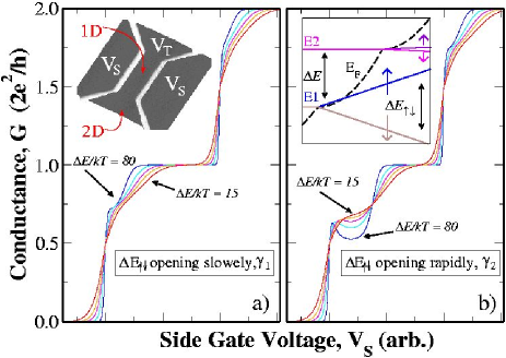
Extending our earlier work Reilly et al. (2002), the phenomenological description is as follows (see inset to Fig. 1(b)). Near pinch-off, at very low gate bias the probability of transmission is equal for both spin-up and spin-down electrons. Our premise is that with increasing gate bias an energy gap forms between up and down spins (or triplet and singlet states) and increases near linearly with 1D density . For the moment we defer discussion of the possible microscopic explanations for this gate dependent spin gap, and focus just on the phenomenology. Key to our model the Fermi-level , where is the electron effective mass and is the Fermi wave vector, is parabolic with density or gate bias since , where is the capacitance between the gate and 1D electrons. Consistent with experimental results Reilly et al. (2001, 2002); Thomas et al. (2000); Pyshkin et al. (2000), at low temperatures this model predicts a feature near when exceeds the spin-down energy but is yet to cross the spin-up band edge. As the temperature is increased the occurrence of a feature closer to is due to the continued opening of the spin-gap with increasing so that the contribution to the current from the thermally excited electrons into the upper-spin band remains approximately constant over a small range in . Although similar in spirit to the model of Bruus et al., Bruus et al. (2000) our picture is based on a spin-gap that is not fixed, but density-dependent and in which and features do not co-exist. Further, in contrast to Fermi-level ‘pinning’ Bruus et al. (2000) the model discussed here suggests that the spin-gap continues to open even as is above the spin-up band-edge.
The only free parameter in this phenomenological model is the rate at which the spin gap opens with gate bias : . This rate governs the detailed shape and position of the feature as a function of temperature. Fig. 1 shows calculations based on this model for two different spin-gap rates, . The conductance is calculated in a very simple way in an effort to show the simplicity of the model. It is assumed that in the linear response regime, with a small bias applied between the left and right leads the conductance is approximated by:
| (1) |
where is the bottom of the band in the left lead, is the Fermi function and are separately the spin-up and down sub-band edges. Assuming that tunneling leads to broadening on a much smaller scale than thermal excitation, we use a classical step function for the transmission probability where for and for . Under this simplification the linear response conductance of each spin-band is well approximated by just the Fermi probability for thermal occupation multiplied by the conductance quantum: .
Comparing Fig. 1(a) and 1(b) we note that the shape of the feature is characterized by both and relative to the 1D sub-band spacing . In Fig. 1(a) a feature near occurs even at low temperatures, since the spin-gap opens slowly () as crosses so that the Fermi function also overlaps by an amount. Contrasting this behavior, Fig. 1(b) illustrates the regime where the spin-gap opens rapidly with (increased ). In this case the low temperature conductance tends towards , after crosses . Increasing the temperature causes the feature to broaden and rise from to .
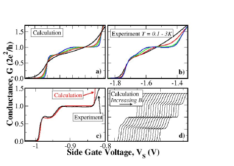
We now turn to compare the results of our model with data taken on ultra-low-disorder QWs free from the disorder associated with modulation doping. Although the fabrication and operation of these devices has been described elsewhere Kane et al. (1998), we reiterate that they enable separate control of both the 2D and 1D densities (see inset Fig1. (a)). Fig. 2(a) and 2(b) compare the calculated temperature dependence of the feature to data taken on a quantum point contact device. The only parameters of the model that were adjusted are the sub-band energy spacing () and the rate at which the spin gap opens () (setting an arbitrary gate capacitance ). As is evident, this model is in good agreement with the shape and dependence of the feature with temperature. Continuing with our comparison between model and experiment, Fig. 2(c) shows data taken on a QW of length at =100mK (black) and calculated conductance based on the model (red), where is now greater than in Fig. 2(a). Note the non-monotonic behavior of the conductance (near ) which we have observed for many of our devices. This oscillatory structure can be traced to the parabolic dependence of and linear dependence of with in the model.
Extending the model to include a Zeeman term: , where is the in-plane electron g factor, is the magnetic field, is the Bohr magnetron and , Fig. 2(d) shows the calculated in-plane magnetic field dependence of the feature. The calculated traces strongly resemble the experimental results of Thomas et al., and Cronenwett et al., Thomas et al. (1996); Cronenwett et al. (2002), in which the feature near evolves smoothly into the Zeeman spin-split plateau at with increasing in-plane magnetic field. A similar but weak dependence is also seen for the feature, where has been reduced in the calculations.
The data shown in Fig. 2(c) was taken with . In comparison to Fig. 2(b) where , the high data (Fig. 2(c)) shows a feature closer to and exhibits non-monotonic behavior. In the context of the model, is the only parameter varied to achieve a fit with both the high and low data.
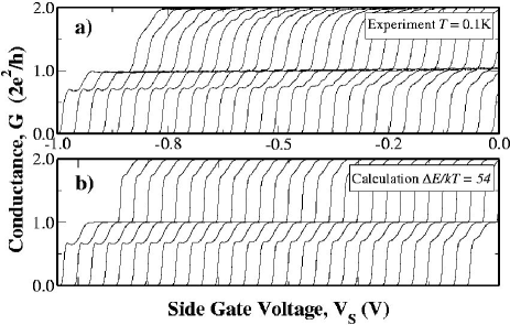
Extending this phenomenological link between and , Figs. 3(a) & 3(b) compare the model with additional data taken on a QW at =100mK. The different traces shown in each of the Figures correspond to an increasing top gate bias or (right to left) for the experimental data and an increasing spin gap rate (right to left) for the calculations. With increasing (data) or (calculations) the conductance feature exhibits an evolution from a slight shoulder feature near to a broader feature, approaching .
The dependence of the feature with has long been debated, with different groups observing conflicting results Thomas et al. (1998); Reilly et al. (2001); Nuttinck et al. (2000); Pyshkin et al. (2000); Thomas et al. (2000). We now present results that indicate that the strength and position of the feature is linked not to the absolute value of , but to the mis-match between the potential of the 1D and 2D regions. Fig. 4 shows data taken on a QW in which is fixed at and is swept negative, reducing the conductance (see Fig. 4 inset diagram). Traces from left to right correspond to sweeps, as is stepped more negative and () is held constant. The effect of stepping negative is to increase the electrostatic confinement, making the relative potential difference between the 2D and 1D regions larger. Similar to the data in Fig. 3, the feature grows in strength and lowers in conductance as is stepped negative, although in this case is not varied. Unlike the behavior expected from an impurity in the 1D channel, these results are reproducible when and are interchanged and the direction of the side-gate confinement potential is reversed. This data indicates that the position and strength of the feature depends not on the absolute value of , but the relative difference between the 1D and 2D potentials.
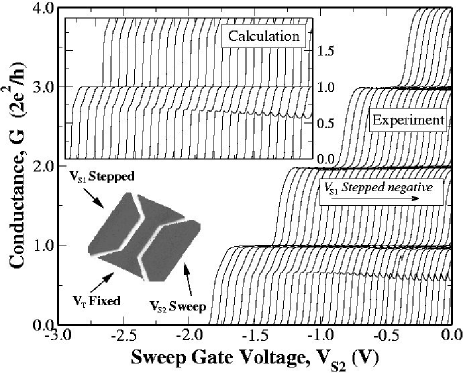
Returning to the phenomenological model, we again draw a link between the 1D-2D potential profile and . The inset to Fig. 4 shows calculations based on the model for differing values of , spanning the regime shown in the experimental results (main plot Fig. 4). As is increased from left to right the feature evolves from a slight inflection to a strong non-monotonic feature consistent with the experimental data.
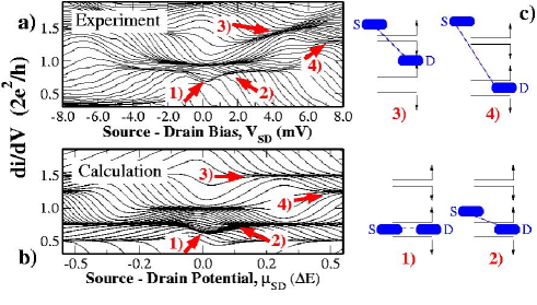
Finally we compare our phenomenology with the dependence of the feature with applied source - drain (SD) bias. Such measurements are key since they permit the evolution of the 1D band-edge energies to be studied as a function of . Fig. 5 compares the differential conductance () of a QW (Fig. 5(a)) to calculations based on the model (Fig. 5(b)). For small equation (1) for the conductance can be extended to finite , where is a weighted average of two zero- conductances, one for a potential of , and the other for , where characterizes the symmetry of the potential drop across the QW Martín-Moreno et al. (1992). In line with this picture Fig. 5(c) is a schematic showing the energies of the S and D potentials relative to the spin-band edges, in connection with the conductance features shown in the data and calculations. Case (1) corresponds to a =0 conductance of which increases to with the application of a bias as shown in case (2). In case (3), the S and D potentials differ by one sub-band (two spin-bands) and the exhibits the well known half-plateaus at due to the averaging of at S () and D ().
Addressing case (4), we focus on the features seen in the data near 8mV (Fig. 5(a)) which are mirrored in the calculations (Fig. 5(b)). To our knowledge, these features have not previously been discussed. In the context of our model the features are due to S and D differing by 3 spin-bands and provide evidence that the spin energy gap remains open well below the Fermi level. Below the first plateau a cusp feature is observed in both the data and calculations shown in Fig. 5 case (1). In the context of our model this cusp arises as the spin gap opens with so that a larger SD bias is needed before S (or D) cross , and increase the conductance. In regard to this cusp feature, we again note the remarkable resemblance between the experimental data and calculations based on the model.
Having presented our model and shown it to be in excellent agreement with experimental data taken on ultra-low-disorder QWs, we now discuss microscopic explanations that may under-pin this phenomenology. These include spontaneous spin polarization Wang and Berggren (1996), the Kondo effect Meir et al. (2002); Hirose et al. (2003); Cronenwett et al. (2002), backscattering of electrons by acoustic phonons Seelig and Matveev (2003) and Wigner-crystallization Matveev (2004). The notion of a spontaneous spin polarization, originally suggested by Thomas et al., Thomas et al. (1996) has remained controversial in connection with exact theory forbidding a ferromagnetic ground state in 1D Lieb and Mattis (1962). This issue however, is complicated by the presence of 2D reservoirs that contact the 1D region and recent calculations Starikov et al. (2003) that include reservoirs suggest a bifurcation of ground and metastable states in association with a spin polarization. The existence of a spin-gap in connection with such a polarized state provides a conceptual picture underlying the phenomenology presented here.
Our phenomenology may also be consistent with a Kondo-like mechanism recently proposed to explain the feature Lindelof (2001); Meir et al. (2002); Hirose et al. (2003). In the context of a Kondo picture the model discussed here is suggestive of a scenario just above the Kondo temperature , where spin screening is incomplete and a (charging) energy gap develops between singlet and triplet states. Recent measurements by de Picciotto et al., de Picciotto et al. (2004) also point to the importance of screening. Perhaps the dependence of on and the sensitivity of the feature to the 2D-1D coupling is linked to , which is a function of the hybridization energy associated with electrons tunneling from the reservoirs into the QW Meir et al. (2002). Note however, that the cusp feature occurring at finite SD bias (discussed above), is in contrast to the Kondo-like zero-bias anomaly (ZBA) observed by Cronenwett et al., below 100mK Cronenwett et al. (2002). At 300mK however, the ZBA seen by Cronenwett et al., evolves into a cusp feature like that seen in our data and calculations (see Fig. 2(a) in Cronenwett et al. (2002)), presumably due to a cross-over from to . Previous investigations indicate the strength of the cusp is strongly dependent on Reilly et al. (2002). In this sense the absence of a ZBA in our results maybe linked to the difference in (relative to the 1D potential) between our samples and those examined by Cronenwett et al., ( for Cronenwett et al., and for our wire shown in Fig. 5(a)). Such an interpretation is again consistent with being a function of or the 2D-1D coupling. In the context of our phenomenology this implies is related to .
Interestingly, a similar temperature dependent cross-over has been described in the theoretical work of Schmeltzer, where a short QW is coupled to Luttinger liquid leads Schmeltzer (2002) (see also Bartosch et al. (2003)). Further, recent work by Seelig and Matveev Seelig and Matveev (2003); Matveev (2004) also describes a temperature dependent correction to the conductance and the presence of a ZBA as arising from the backscattering of electrons by acoustic phonons and in connection with Wigner-Crystallization. Although suggestive, further work is needed to see how these pictures might relate to the phenomenology discussed here. Finally we also mention that calculations based on our model (not shown) are in excellent agreement with the recent high- data of Graham et al., Graham et al. (2003) and the shot noise measurements of Roche et al., Roche et al. (2004). This agreement provides a further indication that our phenomenology is of general relevance and not unique to our samples or experiments.
In conclusion, a phenomenological model has been shown to be in excellent agreement with data taken on ultra-low-disorder QWs. In comparing model and experiment, the only free parameter of the model, , appears to be linked to the potential mis-match between the 2D reservoirs and 1D region. This model provides a means of linking detailed microscopic explanations to the functional form of the conductance feature uncovered in experiments. Such a link is of crucial importance if this effect is to be exploited in novel spintronic devices.
This work was supported by the Australian Research Council. The Author would like to acknowledge a Hewlett-Packard Fellowship and thank Y. Meir, K-F. Berggren, C. M. Marcus and B. I. Halperin for numerous helpful conversations and T. M. Buehler, J. L. O’Brien, A. J. Ferguson, N. J. Curson, S. Das Sarma, A. R. Hamilton, A. S. Dzurak and R. G. Clark for fruitful discussions. The Author is indebted and thankful to L. N. Pfeiffer and K. W. West of Bell Laboratories for providing the excellent heterostructures that lead to this work.
References
- (1) email: djr@phys.unsw.edu.au
- van Wees et al. (1988) B. J. van Wees et al., Phys. Rev. Lett. 60(9), 848 (1988).
- Wharam et al. (1988) D. A. Wharam et al., J. Phys. C 21(8), L209 (1988).
- Thomas et al. (1996) K. J. Thomas et al., Phys. Rev. Lett. 77(1), 135 (1996).
- Kristensen et al. (2000) A. Kristensen et al., Phys. Rev. B 62, 10950 (2000).
- de Picciotto et al. (2004) R. de Picciotto et al., Phys. Rev. Lett. 92, 036805 (2004).
- Morimoto et al. (2003) T. Morimoto et al., Appl. Phys. Lett. 82, 3952 (2003).
- Bird and Ochiai (2004) J. P. Bird and Y. Ochiai, Science 303, 1621 (2004).
- Biercuk et al. (2004) M. J. Biercuk et al., arXiv:cond-mat/0406652 ? (2004).
- Reilly et al. (2001) D. J. Reilly et al., Phys. Rev. B 63, R121311 (2001).
- Cronenwett et al. (2002) S. M. Cronenwett et al., Phys. Rev. Lett. 88, 226805 (2002).
- Meir et al. (2002) Y. Meir, K. Hirose, and N. S. Wingreen, Phys. Rev. Lett. 89, 196802 (2002).
- Cornaglia and Balseiro (2003) P. S. Cornaglia and C. A. Balseiro, arXiv:cond-mat/0304168 (2003).
- Hirose et al. (2003) K. Hirose, Y. Meir, and N. S. Wingreen, Phys. Rev. Lett. 90, 026804 (2003).
- Matveev (2004) K. A. Matveev, Phys. Rev. Lett. 92, 106801 (2004).
- Seelig and Matveev (2003) G. Seelig and K. A. Matveev, Phys. Rev. Lett. 90, 176804 (2003).
- Starikov et al. (2003) A. A. Starikov, I. I. Yakimenko, and K.-F. Berggren, Phys. Rev. B. 67, 235319 (2003).
- Reilly et al. (2002) D. J. Reilly et al., Phys. Rev. Lett. 89, 246801 (2002).
- Thomas et al. (2000) K. J. Thomas et al., Phys. Rev. B. 61(20), R13365 (2000).
- Pyshkin et al. (2000) K. S. Pyshkin et al., Phys. Rev. B. 62, 15842 (2000).
- Bruus et al. (2000) H. Bruus, V. V. Cheianov, and K. Flensberg, Physica E ? (2000).
- Kane et al. (1998) B. E. Kane et al., Appl. Phys. Lett. 72(26), 3506 (1998).
- Thomas et al. (1998) K. J. Thomas et al., Phys. Rev. B 58(8), 4846 (1998).
- Nuttinck et al. (2000) S. Nuttinck et al., Jpn. J. Appl. Phys. 39, L655 (2000).
- Martín-Moreno et al. (1992) L. Martín-Moreno et al., J. Phys. C 4, 1323 (1992).
- Wang and Berggren (1996) C.-K. Wang and K.-F. Berggren, Phys. Rev. B 54(20), R14257 (1996).
- Lieb and Mattis (1962) E. Lieb and D. Mattis, Phys. Rev. 125, 164 (1962).
- Lindelof (2001) P. E. Lindelof, Proc. SPIE Int. Soc. Opt. Eng. 4415, 77 (2001).
- Schmeltzer (2002) D. Schmeltzer, arXiv:cond-mat/0211490 (2002).
- Bartosch et al. (2003) L. Bartosch, M. Kollar, and P. Kopietz, Phys. Rev. B. 67, 092403 (2003).
- Graham et al. (2003) A. C. Graham et al., Phys. Rev. Lett. 91, 136404 (2003).
- Roche et al. (2004) P. Roche et al., arXiv:cond-mat/0402194 ? (2004).