Shot noise in tunneling through a single quantum dot
Abstract
We investigate the noise properties of a zero-dimensional InAs quantum dot (QD) embedded in a GaAs-AlAs-GaAs tunneling structure. We observe an approximately linear dependence of the Fano factor and the current as function of bias voltage. Both effects can be linked to the scanning of the 3-dimensional emitter density of states by the QD. At the current step the shape of the Fano factor is mainly determined by the Fermi function of the emitter electrons. The observed voltage and temperature dependence is compared to the results of a master equation approach.
pacs:
73.63.Kv, 73.40.Gk, 72.70.+mThe so called shot noise has been discussed initially for vacuum tubes, where the current through the device fluctuates due to the stochastic nature of the electron emission process. Schottky (1918) A comparable semiconductor device is a single tunneling barrier and the observed shot noise follows the same expression as that in a vacuum tube: Its noise power density is proportional to the average current with being the electron charge. Blanter and Büttiker (2000) However, it has been shown that the amplitude of the shot noise for resonant tunneling through a double-barrier structure is suppressed in relation to the so called Poissonian value . The occurrence of a suppression is independent from the dimensionality of the resonant state: It has been observed for the first time in quantum well structures where the tunneling takes place through a 2-dimensional subband. Li et al. (1990); Liu et al. (1995) Later experiments in systems containing 0-dimensional states did also show a suppression of the shot noise amplitude below the Poissonian value. Birk et al. (1995); Nauen et al. (2002) This suppression is caused by an anti-correlation in the current due to the finite dwell time of the resonant state in the tunneling structure. Chen and Ting (1991); Davies et al. (1992).
In this paper we present noise measurements on self-assembled InAs quantum dot (QD) systems. These samples provide ideal conditions for measuring the characteristics of single 0-dimensional states since different individual QDs can be selected for transport by applying different bias voltages between the source and drain contacts Narihiro et al. (1996); Itskevich et al. (1996); Hapke-Wurst et al. (2000). In a previous paper Nauen et al. (2002) we examined transport through an ensemble of quantum dots. Now we explore the regime of transport through an individual quantum dot in detail.
The active part of our samples consists of a GaAs-AlAs-GaAs resonant tunneling structure with embedded InAs QDs of 10-15 nm diameter and 3 nm height. Hapke-Wurst et al. (1999) These QDs are situated between two AlAs barriers of nominally 4 nm (bottom) and 6 nm (top) thickness. The thicker barrier is partially penetrated by the InAs QDs. This results into an effective width of 3-4 nm which is slightly thinner than the bottom barrier. A 15 nm undoped GaAs spacer layer and a GaAs buffer with graded doping on both sides of the resonant tunneling structure provide three-dimensional collector and emitter electrodes. Connection to the active layer is realized by annealed Au/Ge/Ni/Au contacts.
About one million QDs are placed randomly on the area of an etched diode structure of area. However, it has been proven that only a small fraction () of these QDs is actually able to participate in the electronic transport. Hapke-Wurst et al. (2003)
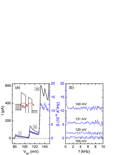
(b) Typical noise spectra of the sample for different bias voltages. The data is smoothed with a 120 Hz boxcar average. The fluctuations of the signal increase with frequency due to the capacitive loading of the current amplifier.
A diagram of the conduction-band profile with one InAs QD embedded in an AlAs barrier is sketched in the inset of Fig. 1a. Due to the small size of the InAs dots the ground state energies of all QDs are larger than the Fermi energy without applied bias voltage. When applying a finite bias the zero-dimensional states of the QDs inside of the AlAs barrier can be populated by electrons and a current through the structure sets on. The largest quantum dots at the tail of the size distribution with lowest energy are first getting into resonance. The small number of ’largest’ dots adds the additional selection for measuring transport through single InAs QDs.
A typical current-voltage (-) curve is shown in Fig. 1a. We observe a step-like increase of at bias voltages mV. Each one of these current steps corresponds to the emitter Fermi energy getting into resonance with the ground states of different individual QDs.
For positive bias voltages the electron tunnels first from the back contact through the thicker bottom barrier onto the resonant state and then through the effectively thinner barrier to the front contact. Thus the emitter tunneling rate is smaller than the collector tunneling rate and the dot is mostly empty. Therefore, the emitter tunneling rate dominates the current and allows us to study the influence of the emitter on the noise properties.
For the noise measurements the sample is mounted into a specially crafted holder that reduces the stray capacitance. This is necessary since the current noise is measured by a low-noise current amplifier that tends to increase its internal noise in case of capacitive loading. We used a current amplifier with bandwidth 10 kHz and inherent noise level of nominally 10 . The output signal is fed into a Fast-Fourier-Transform analyzer for spectral decomposition. The sample holder itself is installed in a 4He-cryostat with a variable temperature insert that can be flooded with liquid helium.
In Fig. 1b we show noise spectra for different applied bias voltages after subtraction of the intrinsic amplifier noise and correction of the amplifier gain. Frequency dependent noise appears only for high bias and kHz. For kHz we observe for the complete voltage range of interest frequency-independent shot noise. We determine the shot noise amplitude by averaging the spectrum from 1 to 10 kHz. The resulting voltage dependence of the shot noise amplitude is shown by the open circles in Fig. 1a.
In order to characterize the amplitude of shot noise one usually compares the measured values to the Poissonian value which is observed for tunneling through a single barrier for . The scale of the right axis in Fig. 1a was chosen in such a way that the black line corresponds to the full Poissonian shot noise. The comparison reveals a suppression of the measured shot noise beneath which can be understood as follows: As long as the ground state of a QD is occupied the tunneling of an additional electron from the emitter is forbidden, resulting in an anti-correlation of successive tunneling events on a timescale corresponding to the dwell time of the resonant state. This makes the transport process less “randomized” and consequently the shot noise is reduced.Nauen et al. (2002)
We will now concentrate onto the two well resolved steps at mV and 110 mV, denoted with (I) and (II). Fig. 2a focuses onto this part of the --curve. With increasing voltage the dot energies are lowered with respect to the emitter (lever arm ). For each resonance level crossing the Fermi energy from empty to occupied emitter states we observe first a step like increase of the current. With further decreasing energy the current drops linearly as indicated by the dashed lines. This nicely matches the prediction of Liu and Aers Liu and Aers (1988, 1989) for resonant 3d-0d-3d tunneling.
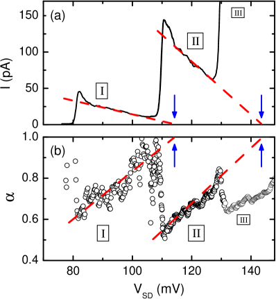
(b) Measured Fano factor of the InAs QDs. The data have been smoothed with a 5-point boxcar average. Again the dashed lines are guides to the eye for the linear behavior.
The observed linear decrease of the current is related to the scanning of the density of states (DOS) of the 3-dimensional emitter by the QD ground state. We can describe this in terms of energy resp. voltage dependent tunneling rates of emitter and collector. Neglecting the energy dependence of the wave function overlap Liu and Aers (1989) the tunneling rates are proportional to the area in momentum space satisfying energy conservation. Liu and Aers (1988) Thus depends linearly on distance of the dot energy to the conduction band edge . Assuming due to the asymmetric barriers the current acquires the observed linear dependence.
For our sample with a Fermi energy meV and an energy-to-voltage conversion factor of the current falls back to zero when the distance to the onset voltage exceeds mV, since then the QD ground state with energy moves below the conduction band edge of the emitter. This agrees with the extrapolation of the current plateau by the dashed lines towards in Fig. 2a.
The afore mentioned approximate linear dependence of the current is mirrored in the behavior of noise properties. In Fig. 2b we plot the Fano factor defined as the ratio of the measured noise to the full Poissonian shot noise . At the step edges of the current we observe maximal noise suppression resp. minimal . With further increase of the Fano factor rises approximately linearly until the next quantum dot comes into resonance. In a previous experiment Nauen et al. (2002) the quick succession of new QDs lead to the observation of a series of peaks in . In the present sample the large spacing of the quantum dot energies allows to observe and extrapolate the linear dependence of the Fano factor for a single resonance. We find a value for the same value at which the current vanishes.
We can calculate the expected Fano factor using a master equation approach following Kiesslich et al. Kiesslich et al. (2003a, b) For a spin degenerate ground state and forbidden double occupancy due to Coulomb blockade we find
| (1) |
Here we have set and for the emitter and collector Fermi functions. In the second step we kept only terms of order . We also omit the voltage dependence of as it changes only weakly in the relevant -window: Due to the large bias voltage the electrons tunnel into collector states at energies high above the Fermi energy and the conductance band edge. The change in the collector tunneling rate is only of order for a change of from the step edge to vanishing current for a single resonance.
With Eq. 1 we easily understand that the linear behavior of the Fano factor has the same origin as the linear behavior of the current, namely the linearly vanishing tunneling rate with the voltage at which crosses . Near this point and we observe essentially single barrier tunneling with full Poissonian shot noise and thus .
The smallest value of the Fano factor of shows up at the current step edge of QD (II) in Fig. 2. Following Eq. 1 this corresponds to an asymmetry of the tunneling rates . In case of QD (I) the asymmetry is increased since the maximal suppression is , corresponding to . This difference most likely stems from the height distribution of the InAs QDs resulting in differing effective thicknesses of the collector barrier.
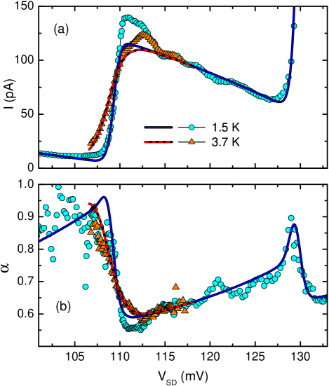
We will now concentrate our analysis onto the temperature dependence of transport through QD (II) which yields a larger current and thus a stronger noise signal. Fig. 3 displays the measured current and Fano factor for two different temperatures. The temperature affects mainly the step edge: When shifting the resonant level through the Fermi energy the current changes smoothly due to the finite width of the Fermi function. In a first approximation this could be modelled by a voltage and temperature dependent tunneling rate with the area in momentum space as described above and the Fermi function. In this descriptive approach the tunneling rate is proportional to the occupied density of states fulfilling energy conservation. For a more rigid evaluation we use a master equation approach Kiesslich et al. (2003a, b) which yields the following formulas for the current and the Fano factor :
| (2) |
| (3) |
The equations were derived for a spin degenerate quantum dot with forbidden double occupancy due to Coulomb energy.
In order to fit the theoretical expression for the current (Eq. 2) and the Fano factor (Eq. 3) to the experimental data we use the following procedure: The ratio of the tunneling rates at the step edge is deduced from the Fano factor while the absolute value is gained from a fit of the current. The lever arm and the dot energy were chosen for a best match of the step edge, and the linear extrapolation of regarding to the scanning of the emitter DOS was fitted to the further evolution of the Fano factor on the current step. For best agreement we include the contributions of QD (I) and QD (III) which are relevant at the onset of current through QD (II) and for mV where transport through QD (III) sets in. As described in Ref.Nauen et al. (2002) for transport through multiple dots we use and with and for each dot given by equations 2 and 3.
In Fig. 3 we show the results of the afore discussed procedure for current and Fano factor in comparison to the experimental data for two different temperatures. It is evident that both the current through QD (II) and the corresponding noise suppression can be described satisfactorily by the above sketched model. Also the peak in the Fano factor at mV is well described by the sum of contributions from QD (II) and QD (III) which confirms Ref. Nauen et al. (2002) where several peaks in were observed at each onset of current through an additional quantum dot.
This dependence of the Fano factor on underlines unambiguously that the suppression of the shot noise is indeed linked to the ratio of the tunneling rates since due to the 3d-0d-3d tunneling in our experiment we are able to tune in relation to . Furthermore we can conclude that the crossover from full shot noise into the suppression is, just as the step edge of the current, governed by the Fermi function of the emitter.
Nevertheless, we observe some deviations from our simple model and we will discuss these now: We observe some fine structure in the current and the shot noise in the ’plateau’ region which is caused by the fluctuations of the local density of states of the emitter. Schmidt et al. (2001)
However, the main difference between the experiment and the theoretical model is the overshoot of the current directly after the step edge for . Most probably this is related to a Fermi-edge singularity (FES) that was shown to enhance the tunneling near the threshold when the QD state is resonant with the emitter Fermi energy. It is caused by a Coulomb interaction of the fluctuating charge on the QD and the emitter electron reservoir. Hapke-Wurst et al. (2000); Geim et al. (1994) Interestingly the Fano factor does also reveal a stronger shot noise suppression below the value given by Eq. 3. For increased temperature the overshoot of the current has virtually vanished as expected for a FES effect. Hapke-Wurst et al. (2000); Geim et al. (1994) Also the additional suppression of the Fano factor below the single particle expectation (Eq. 3) has vanished. Therefore we assume that both features are caused by the same physical process, that is electron-electron interaction.
To conclude, we have measured the shot noise suppression for resonant 3d-0d-3d tunneling through a single InAs QD. We could show that the Fano factor is linked to the ratio of the tunneling rates through emitter and collector barrier, and respectively. We model the observed voltage and temperature dependence of current and shot noise following a master equation approach and find in general a good agreement.
The authors would like to thank Gerold Kiesslich for enlightening discussions.
We acknowledge financial support from DFG and BMBF.
References
- Schottky (1918) W. Schottky, Ann. d. Phys. 57, 541 (1918).
- Blanter and Büttiker (2000) Y. M. Blanter and M. Büttiker, Phys. Rep. 336 (2000).
- Li et al. (1990) Y. P. Li, A. Zaslavsky, D. C. Tsui, M. Santos, and M. Shayegan, Phys. Rev. B 41, 8388 (1988).
- Liu et al. (1995) H. C. Liu, J. Li, G. C. Aers, C. R. Leavens, M. Buchanan, and Z. R. Wasilewski, Phys. Rev. B 51, 5116 (1995).
- Birk et al. (1995) H. Birk, M. J. M. de Jong, and C. Schönenberger, Phys. Rev. Lett. 75, 1610 (1995).
- Nauen et al. (2002) A. Nauen, I. Hapke-Wurst, F. Hohls, U. Zeitler, R. J. Haug, and K. Pierz, Phys. Rev. B 66, R161303 (2002).
- Chen and Ting (1991) L. Y. Chen and C. S. Ting, Phys. Rev. B 43, R4534 (1991).
- Davies et al. (1992) J. H. Davies, P. Hyldgaard, S. Hershfield, and J. W. Wilkins, Phys. Rev. B 46, 9620 (1992).
- Narihiro et al. (1996) M. Narihiro, G. Yusa, Y. Nakamura, T. Noda, and H. Sakaki, Appl. Phys. Lett. 62, 105 (1996).
- Itskevich et al. (1996) I. E. Itskevich, T. Ihn, A. Thornton, M. Henini, T. J. Foster, P. Moriarty, A. Nogaret, P. H. Beton, L. Eaves, and P. C. Main, Phys. Rev. B 54, 16401 (1996).
- Hapke-Wurst et al. (2000) I. Hapke-Wurst, U. Zeitler, H. Frahm, A. G. M. Jansen, R. J. Haug, and K. Pierz, Phys. Rev. B 62, 12621 (2000).
- Hapke-Wurst et al. (1999) I. Hapke-Wurst, U. Zeitler, H. W. Schumacher, R. J. Haug, K. Pierz, and F. J. Ahlers, Semicond. Sci. Technol. 14, L41 (1999).
- Hapke-Wurst et al. (2003) I. Hapke-Wurst, U. Zeitler, U. F. Keyser, R. J. Haug, K. Pierz, and Z. Ma, Appl. Phys. Lett. 82, 1209 (2003).
- Liu and Aers (1989) H. C. Liu and G. C. Aers, J. Appl. Phys. 65, 4908 (1989).
- Liu and Aers (1988) H. C. Liu and G. C. Aers, Solid State Commun. 67, 1131 (1988).
- Kiesslich et al. (2003a) G. Kiesslich, A. Wacker, E. Schöll, A. Nauen, F. Hohls, and R. J. Haug, phys. stat. sol. (c) 0, 1293 (2003a).
- Kiesslich et al. (2003b) G. Kiesslich, A. Wacker, and E. Schöll, Phys. Rev. B 68, 125320 (2003b).
- Schmidt et al. (2001) T. Schmidt, P. König, E. McCann, V. I. Falko, and R. J. Haug, Phys. Rev. Lett. 86, 276 (2001).
- Geim et al. (1994) A. K. Geim, P. C. Main, N. La Scala, L. Eaves, T. J. Foster, P. H. Beton, J. W. Sakai, F. W. Sheard, M. Henini, G. Hill, and M. A. Pate, Phys. Rev. Lett. 72, 2061 (1994).