Also at ]IGNP, Russian Research Center, Kurchatov Institute, Moscow, Russia. Permanent Address: ]Department of Physics, University of Ljubljana, Ljubljana, Slovenia. Also at ]Department of Physics, University of Trieste, Trieste, Italy.
The pseudomorphic to bulk fcc phase transition of thin Ni films on Pd(100)
Abstract
We have measured the transformation of pseudomorphic Ni films on Pd(100) into their bulk fcc phase as a function of the film thickness. We made use of x-ray diffraction and x-ray induced photoemission to study the evolution of the Ni film and its interface with the substrate. The growth of a pseudomorphic film with tetragonally strained face centered symmetry (fct) has been observed by out-of-plane x-ray diffraction up to a maximum thickness of 10 Ni layers (two of them intermixed with the substrate), where a new fcc bulk-like phase is formed. After the formation of the bulk-like Ni domains, we observed the pseudomorphic fct domains to disappear preserving the number of layers and their spacing. The phase transition thus proceeds via lateral growth of the bulk-like phase within the pseudomorphic one, i.e. the bulk-like fcc domains penetrate down to the substrate when formed. This large depth of the walls separating the domains of different phases is also indicated by the strong increase of the intermixing at the substrate-film interface, which starts at the onset of the transition and continues at even larger thickness. The bulk-like fcc phase is also slightly strained; its relaxation towards the orthomorphic lattice structure proceeds slowly with the film thickness, being not yet completed at the maximum thickness presently studied of 30 Å ( 17 layers).
pacs:
68.55.Jk; 61.10.Nz; 79.60.-i; 68.35.RhI Introduction
Heterogeneous epitaxy is a widely exploited technique to fabricate artificial materials, since it allows to introduce a controlled degree of distortion of the interatomic bond length and orientation, which finally allows one to tune the electronic properties of nanostructured devices. In the case of semiconductors, the strain of a film growing on a heterogeneous substrate can be retained up to a thickness of several hundreds of nanometers (coherent growth). Beyond this critical thickness, the strain is released through the formation of a pattern of misfit dislocations, which propagate from the interface to the surface and drive the gradual relaxation (decoherence) of the growing film to its bulk structure. Thanks to the high degree of long range order, the mechanism for semiconductor decoherence can be followed and described in much detail.tsao While a reduced misfit is required for coherent semiconductor growth, thin artificial phases with a lattice structure much different from the bulk one can be stabilized for metal film growth. In the case of oxide substrates, the decoherence of metal films through and ordered network of misfit dislocations is usually observed when the misfit does not exceed 10 %.renaud On the other hand, the metal bonding allows the strain to be released on a much smaller thickness scale, thus reducing the average domain size of the growing film, i.e. the probability of detecting any long range order behaviour. Things are getting more complicated when metal on metal heteroepitaxy is considered, since intermixing phenomena have also to be taken into account, which can either favour the stabilization of pseudomorphic films via surfactant effect (like for the Fe/Au(100) systemopitz ; feau ) or inhibit the coherent growth via substrate roughening and alloying (like for the Co/Cu(111) systemdemiguel ).
In the past ten years, metal heteroepitaxy has been widely applied to study magnetic systems, since the magnetic behavior of metals (both spin orientation and magnetic moment)moroni and their chemical reactivity can be modified by appropriate distortion of their lattice structure. These metastable artificial phases are decomposed into their ground structural phase when the films exceed a critical thickness of a few layers. These transformations are usually observed to be rather sharp and occur through a rather abrupt non-diffusive distortion mechanism, which is accompanied by a strong morphological reorganization, like for the much studied Fe/Cu(100) system,kalki ; fecu thus smearing the mechanisms of domain growth.
In fact, most of the studies have been performed by means of LEED, ion scattering and STM, i.e. surface sensitive techniques. The behavior of the interface and of the layers beneath the surface is poorly known and is usually obtained by photoelectron diffraction (XPD) experiments at a Synchrotron facility, where the photoelectron kinetic energy can be effectively tuned to change the penetration depth. On the other hand, XPD data require a rather complex analysis, whose reliability is hampered when the number of scatterers (penetration depth) is increased.fadley Grazing incidence x-ray diffraction (GIXRD) is certainly the best suited technique to study the structure of a buried interface and the layered structure of thin films.renaud Recently, a combination of XPD and GIXRD techniques has been applied to study the structural dependence on thickness of Fe films on Cu3Au(100) from a pseudomorphic phase to the bcc one.bruno The structural transformation has been shown to be characterized by phase coexistence over a thickness range of a few monolayers.
Hereafter, we have applied GIXRD to study the structure of thin Ni films grown on Pd(100). The epitaxial growth of ultrathin Ni films on the Pd(100) surface has been recently studied by means of LEED, XPS and XPD with a laboratory x-ray source.rizzi This study has shown that in the early stages of the deposition there is the formation of a tetragonally strained face centered (fct) Ni phase with the same lateral lattice spacing of the substrate (i.e. 3.89 Å) and a vertical compression of 0.24 Å. When the film thickness exceeds a critical value of approximately 9-12 layers, the film transforms into its bulk-like Ni fcc structure (lattice parameter of 3.52 Å). The measured strain of the fct phase is found to be in full agreement with the elasticity theory, but some open questions still remain. In particular, although capable to measure very nicely the tetragonal strain adopted by the Ni film, the XPD data did not yield any clear information on how the phase transition develops as the critical thickness is approached nor it was straightforward to extract information on the film/substrate interface. For all these reasons we decided to perform a more detailed study on this system taking advantage of the unique possibilities to acquire both XPS, XPD and GIXRD data offered by the ALOISA beamline at ELETTRA Synchrotron (Trieste Italy).
An effective critical thickness for the pseudomorphic growth has been found. The transformation into the Ni bulk-like structure is shown to involve the interface as well, where the intermixing increases. In addition, the number of layers in the residual pseudomorphic fct phase does not change during the transformation, but simply its domains shrink. The transformation thus proceeds via lateral growth of the bulk-like Ni phase. The increase of the intermixing beyond the critical thickness is attributed to the lateral propagation of the defects, which drive the transformation of the pseudomorphic phase.
II Experimental
Both electron spectroscopy and X-Ray surface diffraction measurements have been performed in situ at the ALOISA beamline, where a wide photon energy range (130-8000 eV), coupled to a multiple detection system, is available.aloisa The UHV experimental chamber (base pressure in the 10-11 mBar range) hosts hemispherical electron analyzers and X-Ray detectors. The emission direction from the sample surface can be freely selected for any orientation of the surface. The sample is mounted on a 6–degrees–of–freedom manipulator, specially designed to select with great accuracy (0.01∘) the orientation of the surface with respect to the incoming photon beam. The temperature of the sample, measured by thermocouples, can be varied by resistive heating and liquid nitrogen cooling.
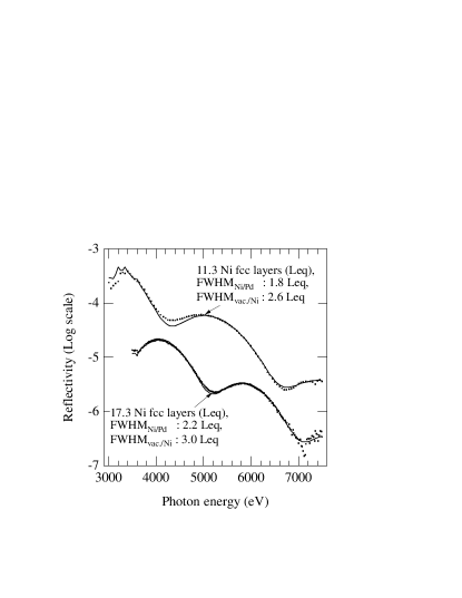
The Pd(100) substrate was prepared by Ar+ sputtering at 1 keV and annealing to 970 K. The substrate order was checked by RHEED, while XPS surveys at grazing incidence (of the order of the critical angle) were used to check for residual contamination. Nickel was evaporated from a carefully outgassed electron bombardment cell (Omicron) provided with a water cooled shield. A quartz microbalance allowed us to tune the deposition flux at a constant rate of 0.6 Å/min (10 % accuracy) before deposition. The absolute calibration of the growth rate was determined a posteriori by measuring the x-ray reflectivity (XRR) at fixed scattering angle while scanning the photon energy between 3 and 8 keV. The interference between the x-ray scattering from the substrate-film and film-vacuum interfaces gives rise to maxima and minima as a function of the perpendicular momentum transfer. Fitting to the XRR curves with a simple model of regularly bulk spaced layers, thus yields the film effective thickness (from the position of maxima and minima) and the width of the interfaces (from the amplitude of the oscillation), as shown in Fig. 1.
For each Ni film, we measured both in-plane XRD and XPS from the Pd 3d core level and the valence band (VB), while XPD polar scans from the Ni 2p3/2 were surveyed for a better comparison with previous experiments. The in-plane XRD measurements consist of radial scans across the ( 0 0) peak in the Pd(100) reciprocal lattice. These measurements were taken scanning the photon energy in a broad range under a suitable - scattering geometry. The observation of diffraction peaks in radial scans allows us to determine the lateral lattice spacing through the Bragg condition . Out-of-plane XRD (rod scans) has been taken for a few selected films in the critical thickness range, to determine the perpendicular distribution of the Ni layer spacings in the pseudomorphic phase. The ( 0 L) rods of the Pd(100) substrate were taken at a photon energy of 7000 eV with a sampling of L =0.03, up to L =2.2. Rod scan simulations were performed by the Vlieg’s program ROD.vlieg
Both Pd 3d and valence band photoemission spectra were taken at a photon energy of 500 eV with a photon energy resolution of meV. The surface was kept at a grazing angle of 4∘, in transverse magnetic (i.e. ) polarization and the electron spectrometer was placed along the surface normal with a kinetic energy resolution of 170 meV. XPD polar scans of the Ni 2p3/2 peak (at h = 1270 eV) were measured in the same scattering conditions by rotating the electron analyzer in the scattering plane. We considered emission along the two main symmetry direction and of the substrate unit cell. We followed the procedure of Ref. bruno2, to extract the anisotropy component from the XPD polar scans by subtracting an isotropic component, which accounts for both geometrical (field of view, illuminated area) and physical (photoemission matrix symmetry, escape depth, surface roughness) factors.
III Results
III.1 Photoemission
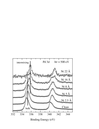
The Pd 3d XPS data (with an overall energy resolution of about 200 meV) are reported in Fig. 2. The Pd 3d5/2 peak of the clean substrate can be fitted with two components, one corresponding to the bulk peak (335.25 eV) and the other to the surface (334.85 eV) , in agreement with previously reported data.todorova Upon Ni deposition the surface component is replaced by an interface one (from 5 Å and beyond), which is shifted by 1.0 eV (335.8 eV) from the bulk component, towards higher binding energies, as can be clearly seen in Fig. 2, where the bulk and interface components are well resolved in the 16 Å thickness film. The bulk component disappears after the deposition of 22 Å of Ni.
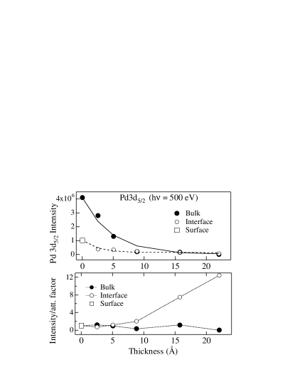
The intensity variation of the Pd 3d5/2 peak with the film thickness is reported in Fig. 3 (upper panel). The bulk and interface components do not follow the same trend. While the bulk component can be nicely fitted with a simple exponential decay, where the only fitting parameter is the Ni film thickness, i.e. the growth rate, the interface component requires a more complex function with an extra parameter , which represents the degree of intermixing between the film and the substrate. It is important to note that the growth rate, as determined from the fitting procedure of the bulk component intensity (0.630.07 Å/min), is in full agreement with the one obtained from the reflectivity curves. The increasing weight of the interface component is well represented in Fig. 3(lower panel), where the ratio between the experimental values and the attenuation law, obtained from the bulk component, is reported. According to the figure, the interface component is the dominating one at 16 Å and beyond.
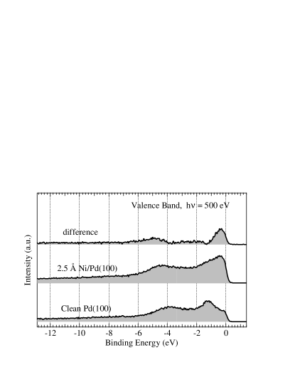
The formation of an intermixed phase already at the beginning of the deposition is also witnessed by the VB photoemission data of Fig. 4, taken just after the deposition of 2.5 Å of Ni. The upper part of the figure shows the difference spectra obtained by subtracting the clean Pd VB spectrum, multiplied by the proper attenuation factor, from the 2.5 Å Ni/Pd(100) spectrum. The result represents the film VB, where the peak at a binding energy of 5 eV cannot be found in the VB of neither pure Ni(100) nor Pd(100). It is worth to remind that the so-called “6 eV satellite” of the Ni 2p spectrum is found shifted to lower binding energies in the 2.5 Å film with respect to the same satellite for a 22 ML thick film.rizzi Both the VB behaviour and the shift to higher binding energy of the Pd 3d5/2 core level are the fingerprint of the intermixing process at the Ni/Pd interface, i.e. to the formation of a NiPd alloy in agreement with literature data.hillebrecht
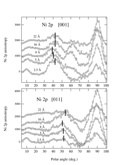
From the structural point of view, the intermixing at the interface determines an enhanced pseudomorphism at the early stages of Ni deposition. This can be observed from the thickness dependence of the forward scattering peaks originated by focussing from close-compact atom row directions in Ni 2p3/2 XPD polar scans, as shown in Fig. 5. At 2.5 Å, the fcc characteristic peaks are closer to the nominal fcc position (at 45∘ and 54.7∘ from the surface normal) than at higher thickness. By increasing the film thickness, the forward scattering peaks shift away from the surface normal, indicating an increase of the vertical compression due to the elastic strain. The strain is released beyond 16 Å by the transformation into the bulk-like Ni structure, in full agreement with previous XPD studies.rizzi
III.2 X-ray diffraction
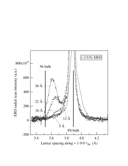
The Ni film transformation from the pseudomorphic fct phase to the bulk-like one does not occur through a continuous relaxation of the strained lattice cell, rather domains of bulk-like symmetry are formed beyond 16 Å, which grow in size as the thickness is increased. This transformation is clearly seen in Fig. 6, where in-plane radial scans across the substrate ( 0 0) XRD peak are shown for a few film thicknesses. Besides the substrate peak, a new feature appears at a thickness of 16 Å, corresponding to a lattice spacing of Å. This feature evolves shortly into a well defined peak (see scan at 22 Å) which gradually shifts towards the 3.52 Å lattice parameter of fcc Ni. The appearance of the Ni bulk-like peak at Å is the fingerprint of a structural phase transition.
For a better understanding of the structural transformation, we have studied the layer spacing distribution in the pseudomorphic fct Ni film. The XRD ( 0 L) rod scans are shown in Fig. 7 for a few films in the range of the critical thickness of 12-16 Å. The XRD scan along the substrate peak rod puts in evidence the x-ray scattering interference between the Ni pseudomorphic layers which are confined between the film-substrate and film-vacuum interfaces. If the deposition is homogeneous on the substrate, well defined interference oscillations can be seen along the rod scans, as in the case of the 8 and 12 Å film thickness. The number of maxima and minima and their position is related to the number of Ni layers in the pseudomorphic structure, while the amplitude of the oscillations to the sharpness of the Ni film interfaces (the larger is the amplitude the sharper is the interface). The increased number of maxima and minima from the 8 Å film to the 12 Å one is thus reflecting the increased number of Ni layers in the pseudomorphic structure. The rod scan taken at 18 Å, where the Ni film structural transition has already started, is still showing a few faint modulations indicating that residual domains of the pseudomorphic phase are still co-existing with the fcc Ni phase. Most strikingly, the maxima and minima of the 18 Å phase still occur at the same perpendicular momentum transfer of the 12 Å film, i.e. the residual domains of the pseudomorphic phase contain the same number of Ni layers. The strong damping of the maxima and minima amplitude indicates both an increase of the pseudomorphic fct phase roughness and the deprival of the pseudomorphic Ni layers due to the shrinking of the corresponding domains. At the thickness of 22 Å, the whole film has been transformed into the Ni bulk-like phase and the rod scan displays a structureless smooth behavior, which is characteristic of a bulk-truncated crystal surface.

The layer spacings and fillings for the 8 and 12 Å films have been obtained by fitting the rod scans with the structural model reported in Table 1. Due to the large number of fitting parameters, we have fixed the inner layer spacings to the value determined by PED analysis after Ref. rizzi, , and we focussed our attention to the substrate-film and film-vacuum interfaces, where XRD yields the best sensitivity. With these constraints, we have found that the topmost layer is also compressed, in excellent agreement with previous XPD studies,rizzi while the layers close to the film-substrate interface are expanded, confirming the vertical pseudomorphism indicated by the present XPD scan on very thin Ni films (Fig. 5). Concerning the buried interface, we admitted Ni/Pd intermixing for two layers. While this model yields an excellent fitting for the thinnest film, a larger number of layers might be affected by the intermixing in the 12 Å film, as indicated by the incomplete layer filling of a few buried Ni layers (3rd to 5th) with respect to the intermediate ones. Alternatively, this finding could be the fingerprint of the formation of extended morphological defects at the Ni-Pd interface, when the critical thickness is achieved.
| 8 Å film | 12 Å film | ||||
|---|---|---|---|---|---|
| layer | spacing | filling | layer | spacing | filling |
| 10th Ni | 1.53 | 0.3 | |||
| 9th Ni | 1.52111fixed parameter, after Ref. rizzi, | 0.7 | |||
| 8th Ni | 1.52111fixed parameter, after Ref. rizzi, | 0.9 | |||
| 7th Ni | 1.52111fixed parameter, after Ref. rizzi, | 0.9 | |||
| 6th Ni | 1.56 | 0.3 | 6th Ni | 1.52111fixed parameter, after Ref. rizzi, | 1.0 |
| 5th Ni | 1.52111fixed parameter, after Ref. rizzi, | 0.7 | 5th Ni | 1.52111fixed parameter, after Ref. rizzi, | 0.9 |
| 4th Ni | 1.52111fixed parameter, after Ref. rizzi, | 0.7 | 4th Ni | 1.52111fixed parameter, after Ref. rizzi, | 0.8 |
| 3rd Ni | 1.86 | 1.0 | 3rd Ni | 1.82 | 0.7 |
| 2nd Ni222intermixed layers | 1.83 | 0.8 | 2nd Ni222intermixed layers | 1.82 | 0.7 |
| 2nd Pd222intermixed layers | 2.07 | 0.2 | 2nd Pd222intermixed layers | 2.05 | 0.2 |
| 1st Ni222intermixed layers | 2.18 | 0.3 | 1st Ni222intermixed layers | 2.08 | 0.3 |
| 1st Pd222intermixed layers | 1.94 | 0.7 | 1st Pd222intermixed layers | 1.90 | 0.7 |
IV Discussion
The evolution of the Ni/Pd(100) film, as a function of the thickness, is described by the following sequence. In the early deposition stage a couple of intermixed layers are formed with strict pseudomorphic structure. Further deposition leads to the formation of strained layers whose lattice cell is pseudomorphic to the lateral substrate lattice, but presents a perpendicular compression in agreement with the elastic force constant model. This elastically strained structure builds up to a critical thickness of 12-16 Å, corresponding to a maximum of 10 layers (including at least 2 intermixed layers at the substrate-film interface), not all of them equally occupied. Beyond this thickness, domains of bulk-like structure are formed and the whole film structure is gradually changed through a first order phase transition. Phase co-existence is clearly observed up to 18 Å. The strain release at the phase transition is not complete and the bulk-like phase gradually relaxes to the orthomorphic fcc phase with increasing thickness.
The formation of a few deposit layers with a full pseudomorphic structure (as indicated by XPD scan in Fig. 5 and rod scan analysis in table 1) was also observed for very thin films (2-3 monolayers) of Fe on Cu3Au(100) bruno ; lin and Ni on Cu(100).mueller The highly strained structure of these layers is probably stabilized by the intermixing and might be a general behavior of metal heteroepitaxy, whenever alloying or surface segregation is chemically favoured. In the present system and before the phase transition, the degree of intermixing remains constant, i.e. the concentration of substrate atoms is much smaller in the next deposited layers. From the 3rd layer on, a compressed vertical spacing is established, in agreement with the value predicted by the elastic theory for the given in-plane expansion, dictated by the substrate lattice.
The sequence of rod scans in Fig. 7 clearly shows that there exists a maximum number of Ni layers that can be stabilized into a pseudomorphic structure (10 layers, included the intermixed ones), thus defining an effective critical thickness for the structural phase transition. This configuration is established at a bulk equivalent thickness of 12 Å. The fact that the maximum number of layers with pseudomorphic fct structure does not change throughout the transition, but simply the fct domains decrease their homogeneity and size, indicates that the transition takes place through the lateral growth of the Ni bulk-like domains at the expense of the pseudomorphic fct phase. Thus the Ni bulk-like domains are not floating on top of the pseudomorphic fct phase nor the transition simply proceeds from top to the bottom, rather, when formed, the Ni bulk-like domains involve locally all the film layers, down to the Ni/Pd interface. A possible model for the Ni bulk-like domains could be that of wedges, with the apex at the substrate-film interface, which expand at the expense of the pseudomorphic phase. Since the phase transition involves three-dimensional domains, it must be of the first order type. No time evolution of the diffracted peaks has been observed at room temperature on the time scale of the experiments (a few hours for the rod scans), which indicates that the transition is kinetically slowed down by the film defects.
At the critical thickness, the intermixing at the Ni/Pd interface (almost constant up to the critical thickness) increases strongly (as indicated by XPS analysis in Fig. 3). It is very tempting to associate the increase of the intermixing with the propagation of a defect from the Ni/Pd interface (whose early formation might be witnessed by the incomplete layer filling of the buried Ni layers at the critical thickness), which drives the transformation of the pseudomorphic fct phase. The Ni/Pd lattice mismatch of 10 %, although not so small, might still allow the formation of an ordered pattern of misfit dislocations originated by the stacking faults at the interface, which would yield characteristic satellites of the Bragg’s peaks in the radial scans.renaud While we have not checked by in-plane XRD for these feature on non-equivalent diffraction peaks other than the ( 0 0) one, LEED pictures taken at the critical thickness were reported to display a Moiré pattern with periodicity.rizzi These patterns clearly show one order of extra spots decorating the integer peaks along the substrate symmetry directions, i.e. the direction of close-compact atom rows on the fcc(100) surface. From comparison with the present data (in particular with the intermixing behaviour), we can say that the strain release indicated by the extra spots is not limited to the Ni film surface, rather the Moiré pattern is originated by defects extending down to the substrate. The Ni/Pd(100) system, where the Ni film undergoes a structural transition between two phases with the same face centered (100) surface symmetry, resembles the behavior of the Fe/Cu(100) system, where a more dramatic structural change, from an fcc(100) to a bcc(110) phase, takes place. In the latter case, the transition of the Fe film was described through the formation of shear planes (from the film surface down to the substrate) along close-compact atom rows, which separate domains of different structural phase, like for a martensitic phase transition.kalki
Concerning the growth of the newly formed bulk-like Ni domains, a mechanism like that driving the decoherence in semiconductor heteroepitaxy can be envisaged. The domain walls, either shear planes or misfit dislocations, propagate laterally on the Pd substrate, leaving behind a strongly intermixed region. This picture is fully consistent with the increase of the Ni/Pd intermixing, which is observed to continue beyond the critical thickness (as indicated both by XPS analysis and by the Ni/Pd interface width obtained by the XRR analysis, Fig. 1)
Finally the newly formed bulk-like Ni film is still strained at small thickness (see radial scan at 22 Å in Fig. 6) and the relaxation to its bulk fcc structure proceeds gradually with increasing thickness. This gradual relaxation, witnessed by the radial scans of the in-plane lattice parameters, is also seen in the perpendicular layered structure of the film. In fact the simple bulk structural models used to simulate the XRR energy scans yields a fitting quality which clearly improves from the 22 to 30 Å film (see Fig. 1). Such a behavior is not surprising, since it has been observed for other metal films. As an example, the bulk structure of Fe deposited on Cu3Au(100) (where the 7% lattice mismatch is even smaller than the present one) is not fully recovered even for film thickness of the order of hundred of monolayers.rochow ; schirmer
V Conclusions
We studied the growth of Ni on Pd(100) by XPS (both core levels and VB), XPD, XRR and XRD (both in- and out-of-plane) techniques. In particular, we followed the structural evolution of the Ni films as a function of the thickness. After the formation of a couple of intermixed layers, (which preserve a perpendicular spacing close to the substrate one) a laterally pseudomorphic phase, with a perpendicular strain in agreement with the elastic theory, takes place. This pseudomorphic fct structure is stable up to 10 layers. Further Ni deposition leads to a gradual structural transformation of the whole film into a Ni bulk-like fcc phase. This phase transition, accompanied by a strong increase of intermixing at the Ni/Pd interface, proceeds through the lateral growth of the Ni bulk-like domains at the expense of the pseudomorphic fct phase. The latter domains preserve their layered structure (maximum number of layers and corresponding spacings), while shrinking. Residual strain is still observed in the Ni bulk-like phase at a thickness of 30 Å.
References
- (1) for an overview of the thermodynamics of semiconductor heteroepitaxy see chapter 5 in Materials Fundamentals of Molecular Beam Epitaxy edited by J.Y. Tsao, Academic Press Inc., San Diego, CA, 1993.
- (2) for an overview of semi-coherent metal/oxide growth see G. Renaud, Surf. Sci. Rep. 32, 1 (1998).
- (3) R. Opitz, S. Löbus, A. Thissen and R. Courths, Surf. Sci. 370, 293 (1997).
- (4) O.S. Hernan, A.L. Vazquez de Parga, J.M. Gallego and R. Miranda, Surf. Sci. 415, 106 (1998).
- (5) J.J. de Miguel, J. Camarero, J. de la Figuera, J.E. Prieto and R. Miranda, in Morphological organization in epitaxial growth and removal, ed. by Z. Zhang and M.G. Lagally, (World Scientific Co., Singapore 1998), p. 367.
- (6) E.G. Moroni, G. Kresse, J. Hafner, J. Furthmüller, Phys. Rev. B 56 (1997) 15629.
- (7) K. Kalki, D.D. Chambliss, K.E. Johnson, R.J. Wilson and S. Chiang, Phys. Rev. B 48, 18344 (1993).
- (8) S. Müller, P. Bayer, C. Reischl, K. Heinz, B. Feldmann, H. Zillgen and M. Wuttig, Phys. Rev. Lett. 74, 765 (1995); J. Giergiel, J. Shen, J. Woltersdorf, A. Kirilyuk and J. Kirschner, Phys. Rev. B 52, 8528 (1995).
- (9) C.S. Fadley Basics Concepts of X-Ray Photoelectron Spectroscopy in Electron Spectroscopy, Theory, Techniques and Applications, C.R. Brundle and A.D. Baker Eds. (Pergamon Press,1978), Volume II, Chapter 1.
- (10) F. Bruno, D. Cvetko, L. Floreano, R. Gotter, C. Mannori, L. Mattera, R. Moroni, S. Prandi, S. Terreni, A. Verdini and M. Canepa, Appl. Surf. Sci. 162-163, (2000) 340; F. Bruno, S. Terreni, L. Floreano, A. Cossaro, D. Cvetko, P. Luches, L. Mattera, A. Morgante, R. Moroni, M. Repetto, A. Verdini, M. Canepa, Phys. Rev. B 66 (2002) 045402.
- (11) G.A. Rizzi, M. Petukhov, M. Sambi, G. Granozzi, Surf. Sci. 522, (2003) 1.
- (12) L. Floreano, et al., Rev. of Sci. Inst. 70, 3855 (1999); R. Gotter, et al., Nucl. Instrum. Meth. Phys. Res. A 467-468 (2001) 1468; An updated presentation of the beamline can be found at http://www.tasc.infm.it/tasc/lds/aloisa/aloisa.html.
- (13) E. Vlieg, J. Appl. Cryst. 33 (2000) 401. The software is freely distributed at http://www.esrf.fr/computing/scientific/.
- (14) F. Bruno, L. Floreano, A. Verdini, D. Cvetko, R. Gotter, A. Morgante, M. Canepa and S.Terreni, J. Elec. Spectrosc. Related Phenom. 127 (2002) 85, cond-mat/0204404.
- (15) M. Todorova, E. Lundgren, V. Blum, A. Mikkelsen, S. Gray, J. Gustafson, M. Borg, J. Rogal, K. Reuter, J.N. Andersen, M. Scheffler, Surf. Sci. 541 (2003) 101.
- (16) F.U. Hillebrecht, J.C. Fuggle, P.A. Bennet and Z. Zolnierek, Phys. Rev. B 27 (1983) 2179.
- (17) M.-T. Lin, J. Shen, W. Kuch, H. Jenniches, M. Klaua, C.M. Schneider and J. Kirschner, Surf. Sci. 410 298 (1998).
- (18) S. Müller, B. Schulz, G. Kostka, M. Farle, K. Heinz and K. Baberschke, Surf. Sci. 364 (1996) 235.
- (19) R. Rochow, C. Carbone, Th. Dodt, F.P. Johnen and E. Kisker, Phys. Rev. B 41, 3426 (1990).
- (20) B. Schirmer, B. Feldmann and M. Wuttig, Phys. Rev. B. 58 4984 (1998).