Possibility of a Metallic Field–Effect Transistor
Abstract
We develop theoretical arguments that demonstrate the possibility of metallic field–effect transistors (METFET’s) in one–dimensional systems and particularly in armchair carbon nanotubes. A very inhomogeneous electric field, such as the field of a tunnelling tip, can penetrate the relatively weakly screened nanotubes and open an energy gap. As a consequence, an energy barrier forms that impedes electron flow and thus permits transistor action. This type of metallic field effect is advantageous because of the high conductance of the metallic tubes in the ON–state.
Field–effect transistors in current use are semiconductor devices. The scaling trend to nanometer dimensions calls for ever higher doping and channel conductance of these devices hessbook . Ultimately one desires a conductance close to that of a metal if one wants to scale devices to the smallest possible size. However, a metallic conductance also prevents the penetration of the electric field except for extremely short distances; ordinarily too short to achieve device function.
We propose here an innovative approach to control electron transport in metallic one–dimensional (1D) systems by use of the inhomogeneous electric field of a low–dimensional highly localized ”modulating” gate (MG) such as nanometer tips or metal nano-interconnects. Use of a highly localized gate results in a strong enhancement of the electric field in a narrow region. Thus any depletion of charge is easier to achieve since it occurs only in extremely small volumes. In addition, the weak screening of electric potentials in 1D channels further enhances possible field effects.
The purpose of this letter is to show that metallic carbon nanotubes may be suitable for use as metallic field–effect transistors (METFET’s). Key to this novel metallic field effect is the opening of a band gap due to the breaking of the mirror symmetry by the MG. Note, that a region of spatially non-uniform electric field also represents a barrier that reflects electrons, while the homogeneous field of an extended gate changes predominantly the carrier density. These qualitative factors are discussed below in a more quantitative way and their potential for device applications is illustrated.
Metallic field effect in Armchair NT’s. – IBM researchers have enunciated the vision of combining metallic and semiconducting single–wall nanotubes (M–SWNT’s and S–SWNT’s) in circuits appenz-utah . The M–SWNT’s would serve as interconnects and the S–SWNT’s as active devices of the extremely small size (typically, the SWNT radius is nm) appenz2 ; appenz ; avouris-r ; avouris . Here we discuss the possibility to also use metallic tubes as transistors or switching devices, which is appealing because of their virtually ballistic conductance pseudos ; lundstr ; appenz2 .
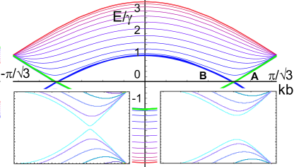
The band structure of an armchair SWNT, as shown in Fig.1, has two subbands A and B (shown as bold green and blue curves) crossing at the Fermi level. Absence of the gap is ultimately related to the SWNT mirror symmetry damnjan , which forbids any mixing of these subbands. We propose to break this mirror symmetry by applying very non–uniform electric fields by use of a MG. Two possible mechanisms for gap opening in armchair SWNTs are: (1) by a direct mixing of electron and hole states of the A and B subbands, which happens if the external potential has an atomic scale corrugation, and (2) by the indirect subband mixing in a higher order of the perturbation theory, which essentially can be realized for any non–uniform potential. Both mechanisms require (i) a relatively high electric field (order of V/cm) and (ii) SWNT symmetry breaking.
Group theory proves that the direct matrix element is non–zero if the Fourier transform of the potential is a full scalar with respect to the rotations of the symmetry group of the nanotube damnjan . This is fulfilled for , where is an positive even integer and is the integer appearing in the notation [n,n] for armchair SWNT’s newyan . Then, the energy dispersion of two new subbands in vicinity of the Fermi point reads as: . Here is the dispersion in A/B subband at zero gate voltage. At the Fermi point and, thus, a gap opens:
| (1) |
This is a direct mixing of the subbands A and B. The bandgap is linear in the applied gate potential (see Inset in Figure 1). A full calculation presenting a selfconsistent solution of joint Schroedinger and Poisson equations following the derivation of Refs. yanli ; jetpl will be published elsewhere. Except for a natural condition that the field must not cause an electric breakdown, there exists no upper limit for the magnitude of the gap that opens in this case and we estimate the possibility of a gap of several eV.
Thus direct mixing of the crossing subbands allows to open a large gap. It does requires, however, a very high multipole moment of the potential in order to break the symmetry (we must at least have ) and this is difficult to achieve because the amplitude of any high multipole component will be typically much smaller than the gate voltage, . Nevertheless, it may be possible to create such a potential by applying the gate voltage to a chemically modified surface of the SWNT. This approach is technologically complex.
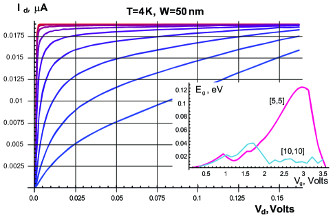
Fortunately, there exists a more straightforward possibility to open a bandgap by virtually any kind of inhomogeneous electric field that breaks the mirror symmetry. A bandgap opens also by indirect mixing of the subbands. This bandgap opening is smaller because it arises from higher order perturbation terms (similar to a nonlinear Stark effect). In particular, any potential that contains both a uniform field and a higher order (quadrupole) component will lead to a gap which scales with the third power of the gate voltage. In what follows we consider an example of two metal tips at opposite sidewalls of the SWNT: one at and the other at bias. The dependence of the bandgap on is shown for [5,5] and [10,10] armchair SWNTs in the Inset of Fig.3. The gap first increases with and decreases beyond where eV is a hopping integral. Perturbation theory yanli ; newyan ; nanotech predicts a maximum gap that depends only on the size of the tube and scales in a universal way for nanotubes of arbitrary chirality:
| (2) |
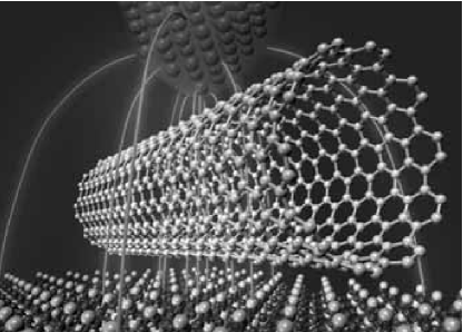
This was confirmed by numerical calculations in Refs.yanli ; nanotech . Here is the Fermi velocity for a M–SWNT, and nm is the bond length. Even though the maximum gap is small in this case and thus has consequences for the conductance only at low temperatures, the gap opening should be much easier to achieve experimentally e.g. by use of the inhomogeneous electric field of a tunnelling tip (Fig.2). Also, ultra narrow leads rotkina , fabricated closely to the nanotube channel, special (electro–)chemical function groups at the tube sidewalls or inside the tube zharov may be used as a MG. We notice that use of a dual gate (both local and backgate) may be beneficial for 1D METFET’s because of the uniform backgate controls the Fermi level (charge density) while the MG controls the conductivity of the channel.
Field effect modulation of metallic conductance. – Any opening of the gate induced semiconductor gap along the armchair metallic tube will create a potential barrier for the electrons and therefore modulate conduction. (Note that this modulation may be enhanced by Coulomb blockade ftft .) Inclusion of tunnelling is important for the calculation of the current because the effective mass of the electrons in SWNT’s is very small (, similar to the in–plane effective mass of graphite ieeenano ). At non zero temperature thermionic emission must be taken into account as well. Although the rate of tunnelling through the classically forbidden (gated) region is high, a significant metallic field effect can be achieved by increasing the width of the gated region, or by operating the device at low source–drain voltage, , and low temperature, . (The ON/OFF current ratio is controlled by the parameter .) Because the transport in the armchair SWNT METFET is ballistic, its conductance in the ON state is limited only by reflections at the contact. We will use in what follows (mainly for normalization purposes) a maximum conductance of ftn .
For the OFF state, we estimate a semiclassical WKB transmission coefficient, , by assuming a uniform gap of width in the gated region. In order to extend the validity of our results to non–zero temperatures we calculate the total transmission of the channel by integrating the partial current, , multiplied by the difference of the Fermi distribution functions of the left and right electrodes.
Figure 3 shows typical IV curves (IVC) for a METFET using a [5,5] armchair M–SWNT of the diameter 0.7 nm at 4K, nm. The upper (red) IVC corresponds to a zero gate voltage (no gap). The channel is fully open and the ON current is determined by injection from a contact and thus by the quantum conductance ftn . With increasing gate voltage one observes a substantial decrease of the current due to the opening of the gap and a depletion of electrons in this region (blue curve). In the Right Inset of Fig.4, the METFET current is plotted vs. the for the dipole–quadrupole potential (two tip geometry) as described above. At low drain bias (blue curve) the METFET is switched OFF at V.
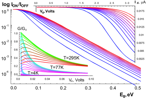
The total transmission coefficient of the METFET, , assuming transparent contacts, is plotted in the Left Inset of Fig.4. Several families of curves are given for different temperatures. In the upper family of curves (room temperature) the suppression of transmission through the gated region is clearly seen as a function of an increased gap: from 0 to 0.12 eV (from green to red, top to bottom). At lower temperatures 77K and 4K this effect is naturally sharper.
The current is an exponential function of the gap (and, hence, of the gate voltage). Results are shown in Figure 4: by opening a gap of about 0.5 eV (which would certainly require sophisticated technology) one can decrease the current by five orders of magnitude.
In conclusion, we have proposed a novel type of electronic switching device based on carbon nanotubes: a one–dimensional metallic field–effect transistor (1D METFET). We have described armchair SWNT’s in detail because of their special symmetry that also gives rise to virtually ballistic transport. Our calculations demonstrate, at least principle, the possibility to open a band gap by application of inhomogeneous electric fields that are created by special gates (modulation gates) that in the simplest case resemble a tunnelling tip to break the SWNT symmetry. Assuming ballistic transport, we have calculated IV curves for the METFET’s with gate widths of the order of 15–50 nm and found significant modulation as well as reasonably large ON/OFF current ratios. We finally note that one can expect excellent scaling properties of the SWNT METFET because of the metallic conductivity enhanced by ballistic transport.
Authors are indebted to Mr. B. Grosser for help with image preparation and Ms. Y. Li for help in numerical computations. This work was supported by NSF Grant No. 9809520, by the Office of Naval Research grant NO0014-98-1-0604 and the Army Research Office grant DAAG55-09-1-0306. SVR acknowledges partial support of DoE Grant No. DE-FG02-01ER45932, and NSF grant No. ECS–0210495.
References
- (1) Advanced Theory Of Semiconductor Devices// Karl Hess. New York: IEEE Press, 2000.
- (2) J. Appenzeller, Device Research Conference, Utah, June 26, 2003
- (3) J. Appenzeller, J. Knoch, R. Martel, V. Derycke, S.J. Wind, Ph. Avouris, IEEE Transactions on Nanotechnology, 1 (4), 184, 2002.
- (4) J. Appenzeller, R. Martel, V. Derycke, M. Radosavljevic, S. Wind, D. Neumayer, and Ph. Avouris, Microelectronic Engineering, 64, 391, 2002.
- (5) Ph.G. Collins, Ph. Avouris, Sci.Am., 12, 62, 2002. Ph. Avouris, Chemical Physics, 281, 429, 2002.
- (6) S. Heinze, J. Tersoff, R. Martel, V. Derycke, J. Appenzeller, Ph. Avouris, Physical Review Letters 89, 106801, 2002.
- (7) P.L. McEuen, M. Bockrath, D.H. Cobden, Y-G. Yoon, and S.G. Louie, Phys. Rev. Lett. 83, 5098, 1999.
- (8) A. Javey, H. Kim, M. Brink, Q. Wang, A. Ural, J. Guo, P. McIntyre, P. McEuen, M. Lundstrom, H. Dai, Nature Materials 1, 241, 2002.
- (9) T. Vukovic, I. Milosevic, M. Damnjanovic, Physical Review B 65(04), 5418, 2002.
- (10) Y.Li, S.V.Rotkin, U.Ravaioli, and K.Hess, unpublished.
- (11) Y.Li, S.V.Rotkin and U.Ravaioli, Nano Letters, 3(2), 183, 2003.
- (12) K.A. Bulashevich, S.V. Rotkin, JETP Letters 75, 205 , 2002.
- (13) S.V. Rotkin, K. Hess, Proc. of Nanotech 2004, Boston, March 7-11, 2004 (in press).
- (14) J.-F. Lin, J.P. Bird, L. Rotkina, P.A. Bennett, Appl. Phys. Lett. 82 (5), 802, 2003.
- (15) S.V. Rotkin, I.Zharov, Int. Journal of Nanoscience 1 (3/4), 347, 2002.
- (16) At the points of metal–semiconductor junction (MSJ) a charge accumulation may happen. This MSJ boundary becomes a side of a 1D capacitor with a capacitance . Neglecting the logarithmic term, a classical charging energy of this capacitor is , which is large for a narrow gate. However, in this work we did not consider a Coulomb blockade because an effective gap is exponentially renormalized at a high conductance of the tunnel junction matveev . Large coupling between sides of the MSJ and quantum fluctuations of the charge wash out the correlation and destroy the Coulomb blockade.
- (17) K.A. Matveev, Phys. Rev. B 51, 1743, 1995.
- (18) The effective mass near the band edge is about 0.06 of the free electron mass for the SWNT of the radius nm.
- (19) For a circuit with macroscopic leads to the M–SWNT channel the total conductance will be about , 4 times of the conductance quantum (for 2 spin and 2 space channels). This gives a minimum resistance of the SWNT device . The lower resistance can be expected in the case of entirely nanotube circuit appenz-utah . The quantum contact resistance will not limit anymore the ON current in this case. That device can fully exploit all advantages of the METFET.