]http://www.riken.jp/lab-www/MQClab/michio/
Single-electron transistors in electromagnetic environments
Abstract
The current–voltage (–) characteristics of single-electron transistors (SETs) have been measured in various electromagnetic environments. Some SETs were biased with one-dimensional arrays of dc superconducting quantum interference devices (SQUIDs). The purpose was to provide the SETs with a magnetic-field-tunable environment in the superconducting state, and a high-impedance environment in the normal state. The comparison of SETs with SQUID arrays and those without arrays in the normal state confirmed that the effective charging energy of SETs in the normal state becomes larger in the high-impedance environment, as expected theoretically. In SETs with SQUID arrays in the superconducting state, as the zero-bias resistance of the SQUID arrays was increased to be much larger than the quantum resistance k, a sharp Coulomb blockade was induced, and the current modulation by the gate-induced charge was changed from periodic to periodic at a bias point , where is the superconducting energy gap. The author discusses the Coulomb blockade and its dependence on the gate-induced charge in terms of the single Josephson junction with gate-tunable junction capacitance.
pacs:
73.23.Hk, 74.50.+r, 74.78.NaPhys. Rev. B 69, 094509 (2004).
DOI: 10.1103/PhysRevB.69.094509
I Introduction
The single-electron transistor (SET), which consists of two small-capacitance tunnel junctions in series and a gate electrode, is an important example of the single-electron-tunneling circuit. Although the SET is more complex than the single junction, the SET has an advantage over the single junction in that the single-electron charging effects typified by “Coulomb blockade” are easily observed in the SET. As a result, the SET can be used, e.g., as an electrometer with an extremely high sensitivity, (e.g., Ref. Averin and Likharev, 1991). When the electrodes of the tunnel junctions in the SET are in the superconducting state, the SET is also important from the viewpoint of quantum computing; the first one-quantum-bit operation in solid-state electronic devices was demonstrated in a circuit with small-capacitance Josephson tunnel junctions, and the state of the quantum bit was read out by measuring the Josephson-quasiparticle (JQP) current of a superconducting SET.Nakamura et al. (1999) The supercurrent of superconducting SETs has also been studied extensively.Joyez (1995) One expects that the supercurrent is periodic in the gate-induced charge. In many experiments, however, a period of has been seen, which suggests the existence of subgap quasiparticle states,Joyez (1995) or “quasiparticle poisoning.” The periodicity of the current was also discussed at finite voltages.Geerligs et al. (1990); Tuominen et al. (1992); Amar et al. (1994) The periodicity depends strongly on how the leads connected to the sample are filtered,Joyez (1995) so that the “quasiparticle poisoning” would be viewed as an environmental effect.
Theoretically,Ingold and Nazarov (1992) the details of single-electron charging effects in SETs depend on the impedance of the electromagnetic environment, , both in the normal state and in the superconducting state. It is predicted that as is increased, the voltage scale of the Coulomb blockade in the normal-state current–voltage (–) characteristics becomes larger, and in the superconducting state, the supercurrent is replaced by the Coulomb blockade. The experimentsJoyez (1995); Geerligs et al. (1990); Tuominen et al. (1992); Amar et al. (1994) on superconducting SETs mentioned above were done in the low-impedance environment, where was much smaller than the quantum resistances: k for Cooper pairs and k for quasiparticles. In order to obtain higher , thin-film resistorsHaviland et al. (1991); Cleland et al. (1992) can be used for the on-chip leads. A superconducting SET was biased with 50 k Cr resistors, and a Coulomb blockade was observed in the – curve.Haviland et al. (1994) Similar resistors ( k) were also employed for the study of Cooper-pair cotunneling in superconducting SETs.Lotkhov et al. (2003) A drawback of these thin-film resistors is that the resistance is not tunable, i.e., the same SET cannot be measured in different environments. A tunable environment has been realized by capacitively coupling a two-dimensional electron gas to a SET.Kycia et al. (2001); Rimberg and Lu (2002) In the work presented here, a simpler method is employed to create tunable environments for superconducting SETs.
We use one-dimensional (1D) arrays of dc superconducting quantum interference devices (SQUIDs) for the on-chip leads,Watanabe and Haviland (2001, 2003) which can be fabricated simultaneously with superconducting SETs. The SQUID configuration enables us to vary in situ the effective impedance of the arrays by applying a weak external magnetic field ( mT) perpendicular to the SQUID loop. The superconducting SET in our samples, on the other hand, does not have a SQUID configuration, and therefore its parameters are practically independent of the external magnetic field. The zero-bias resistance of SQUID arrays at low temperatures can be controlled over several orders of magnitude (e.g., Fig. 13 of Ref. Watanabe and Haviland, 2003), and SQUID arrays are especially suitable for achieving a high-impedance environment. In fact, distinct Coulomb blockade was observed in single Josephson junctions by biasing with SQUID arrays.Watanabe and Haviland (2001) When the sample is driven to the normal state, the array leads are no longer tunable, but the resistance can be much larger than . Hence, it is still possible to study the environmental effects on SETs by comparing the samples with and without array leads. In this paper, the environmental effects on SETs is discussed both in the normal state and in the superconducting state. An emphasis is placed on the case of a high-impedance environment, which has not been thoroughly experimentally studied.
II Experiment
II.1 Fabrication of small-capacitance tunnel junctions
The tunnel junctions (Al/Al2O3/Al) were fabricated on a SiO2/Si substrate with Au/Ni bonding pads. We employed a process based on electron-beam lithography and double-angle shadow evaporation, which is similar to the one described in Ref. Watanabe and Haviland, 2003. The evaporation of Al was done at an rate of nm/s in a vacuum system with the base pressure of Pa. During the evaporation, the pressure was usually Pa. The Al2O3 tunnel barrier was formed by exposing the base Al layer to Pa of O2 for min. before the deposition of the top Al layer. The thickness of the barrier determines the normal-state resistance of the junction per unit junction area. The normal-state resistance is a key parameter of the sample, and will be discussed in Sec. II.3.
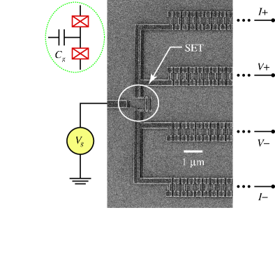
Figure 1 shows a scanning electron micrograph of a sample. The SET is biased with two pairs of leads enabling four-point measurements. A part of each lead close to the SET consists of a 1D array of dc SQUIDs.
II.2 Measurement at low temperatures
The samples were measured in a 3He–4He dilution refrigerator (Oxford Instruments, Kelvinox 400) mainly at K, and the normal-state resistance was determined at K. (Note that the superconducting transition temperature of Al is 1.2 K.) The temperature was calculated from the resistance of a ruthenium-oxide thermometer fixed to the mixing chamber. Magnetic fields on the order of mT were applied by means of a superconducting solenoid. In this magnetic-field range, the temperature error of ruthenium-oxide thermometers due to magnetoresistance is negligibly small (e.g., a typical value of the error at K is less than 0.1%).Watanabe et al. (2001) The samples were placed inside a copper can which was thermally connected to the mixing chamber. Because there was no low-temperature filtering, we inserted low-pass filters between the cables connected to the cryostat and the measurement circuit.
The – curve of the SET was measured in a four-point configuration (see Fig. 1). The bias was applied through one-pair of leads, and the potential difference was measured through the other pair of leads with a differential voltage amplifier (DL Instruments, 1201, G input impedance). The current was measured with a current amplifier (DL Instruments, 1211). The SQUID arrays could be measured in a two-point configuration (same current and voltage leads). When we measure the arrays on the same side of the SET (e.g., and in Fig. 1), current does not flow through the SET, and the series resistance of two arrays is obtained. The zero-bias resistance measured in this configuration will be discussed in Sec. II.3.
II.3 Characterization of the samples
In this work, we measured the three pairs of SETs listed in Table 1.
| Sample | (k) | (k) | (aF) |
|---|---|---|---|
| 1a | 6.0 | ||
| 1b | 5.6 | 6.0 | |
| 2a | 4.8 | ||
| 2b | 4.1 | 4.9 | |
| 3a | 4.8 | ||
| 3b | 1.4 | 4.8 |
Each pair (e.g., samples 1a and 1b) was fabricated simultaneously on the same chip. One SET has SQUID-array leads with junction pairs in each array, while the other SET has no SQUID-array leads (). For all the samples, the junction area was designed to be 0.10.1 m2 in the SET and 0.30.1 m2 in the SQUID arrays.
The uniformity of the SQUID arrays could be estimated by measuring the normal-state resistance in all two-point configurations (six in total). In some configurations, current flows through the SET and thus the normal-state resistance of the SET has to be subtracted from the measured resistance in order to obtain the series resistance of two arrays. For our samples, the results of the two-point measurements agreed with one another within 3%–4%. By averaging all the results, the normal-state resistance per junction pair of the arrays is calculated, and shown in Table 1. If the tunnel-barrier thickness is identical for all junctions on the same chip, one would expect from the junction area. From Table 1, the ratio is , which is the correct order of magnitude.
From the normal-state resistance, I calculate the Josephson energy, which is an important parameter of the samples. For example, the maximum Josephson energy between adjacent islands in the SQUID arrays is given by the Ambegaokar-Baratoff formula,
| (1) |
where is the superconducting energy gap ( meV for Al). Because of the SQUID configuration, the effective Josephson energy in the arrays is modulated periodically by applying an external magnetic field perpendicular to the SQUID loop,
| (2) |
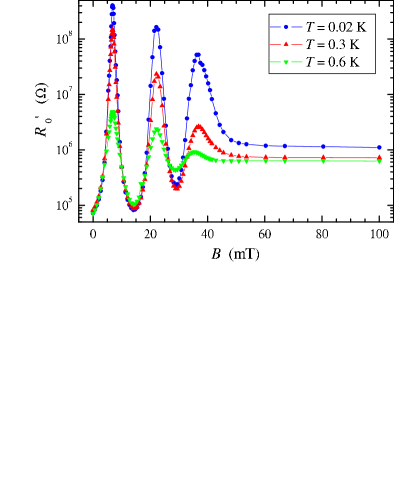
so long as is sufficiently smaller than the critical field, where Wb is the superconducting flux quantum, and is the effective area of the SQUID loop, which is 0.70.2 m2 in our samples. Equation (2) is a key to understand Fig. 2, which shows that the zero-bias resistance of two SQUID arrays in series oscillates as a function of until becomes comparable to the critical field. Note that the first peak appears at mT, where the normalized flux is 0.5 for our samples with m2. In Ref. Haviland et al., 2000, the SQUID array was modeled as a network of capacitors and inductors, and the real part of the array impedance was shown to be proportional to at low enough frequencies. At mT in Fig. 2, the superconductivity is suppressed, and takes a value comparable to . The small temperature dependence in this magnetic-field regime is due to the single-electron charging effect. In general, the – curve of SQUID arrays is nonlinear (e.g., Fig. 3 of Ref. Watanabe and Haviland, 2003), and therefore, SQUID arrays are not described by a linear impedance model.Haviland et al. (2000) However, it would be a good approximationWatanabe and Haviland (2003) to use for characterizing the electromagnetic environment of the SET. I also assume that the SET is in a high-impedance environment when . As for the samples without SQUID arrays, the resistance of the leads is always much smaller than , and the SET is in a low-impedance environment. The Josephson energy in the SET is calculated in a similar way, but note that it does not oscillate as a function of because the junctions in the SET do not have a SQUID configuration.
Another important parameter is the charging energy, which is inversely proportional to the capacitance of the junction. The capacitance can be estimated from the junction area with a specific capacitance on the order of fF/m2. In our samples, the junction area is much larger, or the charging effect is much weaker, in the SQUID arrays than in the SET. In the normal state, for example, the – curve of the SQUID arrays is almost linear (data not shown, similar to the bottom curve in Fig. 3 of Ref. Watanabe and Haviland, 2003) even when the SET shows a well developed Coulomb blockade like in Fig. 6(b), which would be favorable when the arrays are used as leads.
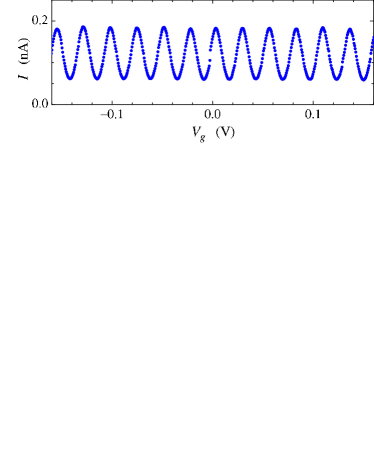
The capacitance between the island electrode and the gate electrode is determined by the period of the gate modulation in the normal state. An example is shown in Fig. 3. Though the design of the SET is the same for all the samples, the values of in Table 1 are divided into two groups: 6 aF for samples 1a and 1b, and 5 aF for the others. The reason could be that we used two SiO2/Si wafers whose thickness of the SiO2 layer is different, and that we fabricated samples 1a and 1b on one wafer ( m) and samples 2a–3b on the other ( m).
III Results and discussion
III.1 Single-electron transistors in the normal state
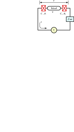
At , the – curve of the SET in the normal state is expected to have a region where . Such a region is called a “Coulomb gap,” and depends not only on the gate voltage but also on the electromagnetic environment.Ingold and Nazarov (1992) The circuit considered in the theoryIngold and Nazarov (1992) is shown in Fig. 4, where and () are the capacitance and the tunnel resistance, respectively, for the th junction, and is the impedance of the electromagnetic environment. The theory assumes that and . In Fig. 4, the gate is not drawn explicitly because when , which is the case in our samples, the influence of the gate can be included in the effective island charge,
| (3) |
where is an integer and is the background charge.
In the theory, the drift of is not considered, and thus for simplicity, in Eq. (3). In the experiment, however, the drift often becomes a problem. In samples 1a, 1b, 3a, and 3b, the drift was usually , which is negligible for the discussion in this paper. In samples 2a and 2b, on the other hand, the drift was not slow enough () compared to the time needed to measure hundreds of – curves at different values of in our experimental setup. Thus, for samples 2a and 2b, we mainly measured vs keeping the source voltage constant.
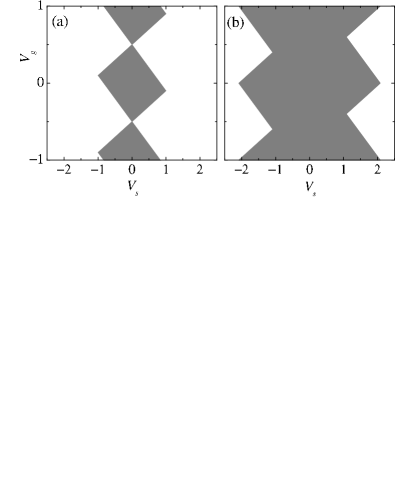
Figure 5 shows the theoretical Coulomb gap on the – plane for (low-impedance environment) and for (high-impedance environment). The Coulomb gap is periodic in for both the cases. However, the magnitude of the gap is different, and e.g., at , the gap in the high-impedance environment is about twice as large as that in the low-impedance environment. It is important to note a qualitative difference at . The gap vanishes in the low-impedance environment, but survives in the high-impedance environment. These theoretical predictions have been confirmed in our experiments. Figure 6 shows the normal-state – curves at K for samples 1a and 1b. We drove the samples into the normal state by applying a magnetic field of 0.1 T perpendicular to the substrate. In the normal state, the SQUID arrays of sample 1b have M at K, and thus, I assume that the SET in sample 1b is in a high-impedance environment. The SET in sample 1a, on the other hand, is in a low-impedance environment because it is not biased with the arrays. In the lower data set (), the size of the Coulomb gap in Fig. 6(b) is about twice as large as that in Fig. 6(a). Moreover, in the upper data set (), the – curve in Fig. 6(a) is linear, i.e., no Coulomb gap, while the curve in Fig. 6(b) still shows a considerable nonlinearity.
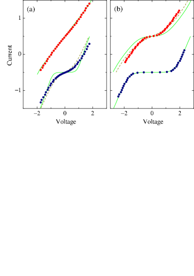
I have also calculated the – curves based on the theory assuming . For the lower data set in Fig. 6(b), a perfect agreement is obtained with , , fF, and ( K), where . These parameters are employed for all the solid curves in Fig. 6. The solid curve does not always reproduce the experimental data very well, but I nevertheless conclude that our experiments have demonstrated the environmental effects predicted by the theory. I emphasize that the solid curves are calculated with the same set of parameters, and the discrepancy is reduced if the parameters are adjusted for the calculation for each data set. The dashed curves for the lower data set of Fig. 6(a) and for the upper data set of Fig. 6(b), which agree better with the experimental data, are obtained by raising the temperature in the calculation to ( K), keeping the other parameters constant.
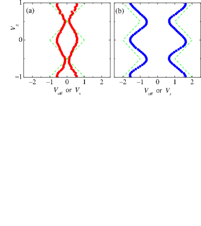
At finite temperatures, nonzero current flows even within the Coulomb gap. Therefore, it is not straightforward to determine the Coulomb gap from the experiment. As an estimate of the Coulomb gap, I have calculated the offset voltage by fitting
| (4) |
to the data in the high-bias regime, for and for . The results for samples 1a and 1b are plotted in Fig. 7 together with the theoretical predictions for the low-impedance environment and high-impedance environment, respectively. Here, I used the same parameters as in Fig. 6. The experimental is consistent with the theoretical prediction.
In fact, one of the assumptions in the theory for the high-impedance case, , is not fulfilled in the experiment. In the normal state, in sample 1b, so that the SET in sample 1b is current-biased. However, I am still convinced that the comparison with the theory is meaningful, because we measured the SET in four-terminal configuration, and because the measured – curves are qualitatively explained within the theory. Furthermore, the parameters used in the calculations for Fig. 6 are reasonable. It is common to observe that the effective electron temperature becomes considerably higher than the temperature of the mixing chamber in the experiments of small-capacitance tunnel junctions.Watanabe and Haviland (2003) The temperature difference is likely to be large when the cryostat leads are not filtered at low temperatures, which is the case in our cryostat. Most importantly, fF is consistent with our junction size, and as I mentioned earlier, much larger than . This value of the total capacitance will be used again in the discussion in Sec. III.2.
III.2 Single-electron transistors in the superconducting state

For the samples with SQUID-array leads, the same superconducting SET can be studied in different electromagnetic environments by changing the external magnetic field on the order of a few mT. In this work, I look at the low-bias region of , where the – curve is sensitive to the state of the electromagnetic environment. In all the samples with SQUID-array leads, the – curve of the superconducting SET developed a Coulomb blockade as was increased by tuning the field. Figure 8 shows the – curves of the SET in sample 1b in two different environments. As I mentioned earlier, the parameters of the SET should be independent of the field, because the SET does not have a SQUID configuration and the field applied in Fig. 8 is much smaller than the critical field. The electromagnetic environment for the SET (the SQUID arrays), on the other hand, is strongly varied with the field as we have seen in Fig. 2. The behavior of the SET demonstrated in Fig. 8 does not result from the magnetic-field influence on the – curve of the SET, but rather from an environmental effect on the SET. I note here that the SETs without SQUID arrays were also measured at and at mT, and that the – curves were almost the same. The well-developed Coulomb blockade in Fig. 8(b) indicates that the SET is in a high-impedance environment, which is consistent with G . From the viewpoint of , the SET is not in a low-impedance environment in Fig. 8(a) because M is already larger than . Thus, in order to study the low-impedance case, we have to measure samples without SQUID-array leads. Rather surprisingly, e.g., in sample 1a, the – curve and its dependence on the gate-induced charge were qualitatively almost the same as Fig. 8(a), and the supercurrent was too small to be seen in the – curve. This is due to “quasiparticle poisoning,” which is likely to occur in our cryostat which has no low-temperature noise filters. In addition, our biasing scheme is not ideal for the supercurrent measurement because the samples without SQUID-array are voltage biased. The supercurrent was not detected in samples 2a or 3a, either.
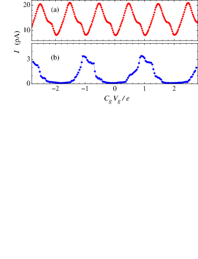
“Quasiparticle poisoning” is also suggested by the periodicity in the current modulation by the gate-induced charge, which was observed in all samples without SQUID-array leads. The periodicity was also found in sample 1b when M, as shown in Fig. 9(a), where the potential drop across the SET is 0.15 mV. When is increased to 0.3 G [Fig. 9(b)], it was replaced by periodicity, which indicates Cooper-pair transport. The SQUID arrays with sufficiently large acted as a filter that suppresses the contribution of quasiparticles to the charge transport. This change in the periodicity was also found in sample 2b. In sample 3b, however, only periodicity was seen probably because the maximum of was only 9 M. The curve in Fig. 9(b) is calculated from the – curves, because we could not fix the potential drop across the SET when it is much smaller than that across the SQUID arrays in our experimental setup.
Below I focus on the case of , and discuss the Coulomb blockade of Cooper-pair tunneling. In the high-impedance environment, a current-biased single Josephson junction is expected theoreticallyAverin and Likharev (1991); Schön and Zaikin (1990) to have a “back-bending” – curve, which has been experimentallyHaviland et al. (1991); Watanabe and Haviland (2001, 2003) confirmed. The “back-bending” is also seen in Fig. 8(b) for certain values of the gate-induced charge. When the “back-bending” is clearly seen in the SET – curve, I define the blockade voltage as the local voltage maximum (minimum) for () in the low-current part of the – curve. The measured is plotted in Fig. 10 as a function of the gate-induced charge. The dotted and broken curves represent at constant calculated from the – curves. These curves would also characterize the Coulomb blockade. The analytic expression of at low temperatures has been obtained for single Josephson junctions as
| (5) |
for , and
| (6) |
for , where is the capacitance of the single junction.
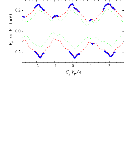
The relationship between a superconducting SET and a single Josephson junction in the low-impedance environment has been discussed,Joyez (1995) and by examining the Hamiltonian, it has been shown that a superconducting SET can be viewed as a single Josephson junction with gate-tunable . I have found a similar relationship for the high-impedance case, which explains the variation of in Fig. 10. In the high-impedance environment, not only the island charge [ in Eq. (3)] but also the total charge seen from the outside contributes to the charging energy,Ingold and Nazarov (1992) where is the charge on the th junction. This is why in Fig. 5, the Coulomb gap is larger in the high-impedance environment. Let us compare Fig. 5(b) with the Coulomb gap for a single junction in the high-impedance environment,Ingold and Nazarov (1992) which is . In this environment, a SET can be viewed as a single junction with gate-tunable or , where the minimum of is and the maximum is . I do not know the exact expression for the effective of the SET in the high-impedance environment, however, the magnitude should be similar to the low-impedance case,Joyez (1995) . From Table 1 and fF, which was obtained from the curve fit in Fig. 6, the effective of the SET in Fig. 10 is always smaller than 0.04 (1). Thus, from Eq. (5), our model predicts that oscillates between 0.08 and 0.16 mV in Fig. 10. The order of magnitude is correct and the gate dependence is explained. Note that the notion of gate-tunable is a key because at , depends only on .
IV Conclusion
The transport properties of single-electron transistors (SETs) have been studied in various electromagnetic environments. In half of the samples, SQUID-array leads were employed in order to realize a magnetic-field-tunable environment in the superconducting state and a high-impedance environment in the normal state. I have demonstrated that the effective charging energy of SETs in the normal state becomes larger in the high-impedance environment than in the low-impedance environment. In the superconducting state, the current modulation by the gate-induced charge changed from periodic to periodic in SETs with SQUID-array leads, as the zero-bias resistance of the leads was increased to be much larger than the quantum resistance k. This change in the periodicity suggests that SQUID arrays with sufficiently large suppress the contribution of quasiparticles to the charge transport. When , a sharp Coulomb blockade appears in the current–voltage characteristics, and the blockade voltage varies depending on the gate-induced charge. The variation of is explained within a model that treats a superconducting SET as a single Josephson junction with gate-tunable junction capacitance in the high-impedance environment.
Acknowledgements.
I am grateful to Y. Nakamura for fruitful discussion and to M. J. Dalberth for proofreading the manuscript. This work was supported by Special Postdoctoral Researchers Program and President’s Special Research Grant of RIKEN, and MEXT.KAKENHI(15740190). Sample fabrication and measurement were done at Semiconductors Laboratory (closed in March, 2003), RIKEN.References
- Averin and Likharev (1991) D. V. Averin and K. K. Likharev, in Mesoscopic Phenomena in Solids, edited by B. L. Altshuler, P. A. Lee, and R. A. Webb (Elsevier Science, Amsterdam, 1991), Chap. 6.
- Nakamura et al. (1999) Y. Nakamura, Yu. A. Pashkin, and J. S. Tsai, Nature (London) 398, 786 (1999).
- Joyez (1995) P. Joyez, Ph.D. thesis, University of Paris 6, France, 1995.
- Geerligs et al. (1990) L. J. Geerligs, V. F. Anderegg, J. Romijn, and J. E. Mooij, Phys. Rev. Lett. 65, 377 (1990).
- Tuominen et al. (1992) M. T. Tuominen, J. M. Hergenrother, T. S. Tighe, and M. Tinkham, Phys. Rev. Lett. 69, 1997 (1992).
- Amar et al. (1994) A. Amar, D. Song, C. J. Lobb, and F. C. Wellstood, Phys. Rev. Lett. 72, 3234 (1994).
- Ingold and Nazarov (1992) G.-L. Ingold and Y. V. Nazarov, in Single Charge Tunneling, edited by H. Grabert and M. H. Devoret (Plenum, New York, 1992), Chap. 2.
- Haviland et al. (1991) D. B. Haviland, L. S. Kuzmin, P. Delsing, K. K. Likharev, and T. Claeson, Z. Phys. B 85, 339 (1991).
- Cleland et al. (1992) A. N. Cleland, J. M. Schmidt, and J. Clarke, Phys. Rev. B 45, 2950 (1992).
- Haviland et al. (1994) D. B. Haviland, Yu. Pashkin, and L. S. Kuzmin, Physica B 203, 347 (1994).
- Lotkhov et al. (2003) S. V. Lotkhov, S. A. Bogoslovsky, A. B. Zorin, and J. Niemeyer, cond-mat/0305113 (2003).
- Kycia et al. (2001) J. B. Kycia, J. Chen, R. Therrien, Ç. Kurdak, K. L. Campman, A. C. Gossard, and J. Clarke, Phys. Rev. Lett. 87, 017002 (2001).
- Rimberg and Lu (2002) A. J. Rimberg and W. Lu, cond-mat/0205382 (2002).
- Watanabe and Haviland (2001) M. Watanabe and D. B. Haviland, Phys. Rev. Lett. 86, 5120 (2001).
- Watanabe and Haviland (2003) M. Watanabe and D. B. Haviland, Phys. Rev. B 67, 094505 (2003).
- Watanabe et al. (2001) M. Watanabe, M. Morishita, and Y. Ootuka, Cryogenics 41, 143 (2001).
- Haviland et al. (2000) D. B. Haviland, K. Andersson, and P. Ågren, J. Low Temp. Phys. 118, 733 (2000).
- Schön and Zaikin (1990) G. Schön and A. D. Zaikin, Phys. Rep. 198, 237 (1990).