[
Temperature dependence and control of the Mott transition in VO2-based devices
Abstract
The transition voltage of an abrupt metal-insulator transition
(MIT), observed by applying an electric field to two-terminal
devices fabricated on a Mott insulator VO2 film, decreases
with increasing temperature up to 334K. The abrupt current jump
disappears above 334 K near the MIT temperature. These results
suggest that the mechanism of the abrupt MIT induced by
temperature is the same as that by an electric field. The
magnitude of the current jump (a large current) decreases with
increasing external resistance; this is an important observation
in terms of applying the abrupt MIT to device applications.
Furthermore, the temperature and resistance dependence of the MIT
cannot be explained by the dielectric breakdown although a current
jump known as breakdown is similar to that observed in an abrupt
MIT.
]
Thin films of vanadium dioxide, VO2, have been extensively studied for electronic and electro-optic device applications [1, 2, 3] of an abrupt first-order metal-insulator transition (MIT) at a critical temperature 340 K [4, 5, 6]. Recently, a new type of abrupt MIT, having an abrupt jump of driving current in a two-terminal device fabricated on an epitaxial VO2 film, has been demonstrated by electric field excitation [7]. The abrupt MIT does not undergo a structural phase transition [8], as predicted by Mott for an abrupt first-order MIT driven by strongly correlated electronic Coulomb energy [9].
When an abrupt MIT occurs and excess current flows in a device, the device can be damaged or its characteristics can be degraded. Furthermore, the electric I-V characteristics of the abrupt MIT are similar to those of dielectric breakdown observed at high electric fields in thin AlOx and HfO2 gate insulators [10, 11]. Clearer evidence of the Mott transition, a control method of the excess current for device applications utilizing abrupt MITs, and evidence of the difference between a breakdown and an abrupt MIT are important unresolved issues in this field.
In this paper, we measure the temperature dependence of abrupt MITs in VO2 driven by a DC electric field to suggest evidence of the Mott transition, and control the magnitude of the abrupt current jump (or excess current) using an external resistance. The effect of measurement on the magnitude of the observed current is briefly discussed. An important difference between a breakdown and an abrupt MIT is also given.
Thin films of VO2 have been deposited on (1102) Al2O3 and Si substrates by laser ablation [12]. The thickness of the VO2 films is about 900 Å. For two-terminal devices, Ohmic-contacted Au/Cr electrodes on VO2 films with a channel width of 25 and a channel length of 5 were patterned by photo-lithography and lift-off. I-V characteristics of the devices were measured by a precision semiconductor parameter analyzer (HP4156B).
Figure 1 (a) shows the temperature dependence of the resistance of an epitaxial VO2 film I. The resistance
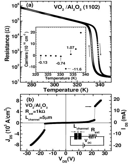
decreases with increasing temperature and shows an abrupt MIT at a critical temperature 340 K (68∘C). This is consistent with previous measurements [4, 5]. It was proposed that this abrupt MIT is due to the structural phase transition from monoclinic below to tetragonal above [13, 14]. The decrease of the resistance up to 340 K indicates an increase of hole carriers, and two kinds of electron and hole carriers coexist near 340 K, as shown in the inset of Fig. 1 (a). Owing to a mixing of electrons and holes, the number of carriers at temperatures from 332 to 340 K is not exactly determined. The number of hole carriers at 340 K is expected to be 3 1018 cm-3 from the Mott criterion [1, 9], based on an exponential decrease of resistance (increase of carrier) with increasing temperature. corresponds to 0.018% of -band charges. In the metal regime above 340 K, the major carriers are electrons, as shown in the inset of Fig. 1 (a). Fig. 1 (b) shows the drain-source-voltage dependence of conducting current, , density, , of the flow between two terminals (drain-source) for a VO2 film II. An abrupt current jump near the transition voltage = 20 is shown and Ohmic behavior as a characteristic of metal is also exhibited over the transition voltage. This is a typical characteristic of a first-order transition and is reproducible more than 1,500 times.
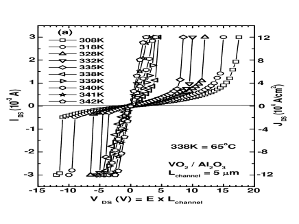
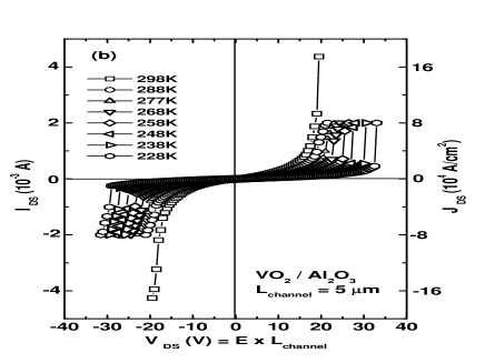
Figures 2 (a) and (b) show the temperature dependence of the abrupt MIT measured at device II fabricated on a VO2/Al2O3 film III. The transition voltage of the abrupt MIT decreases with increasing temperature. This arises from excitation of hole charges by temperature. At 338 K, near the transition temperature of the abrupt MIT, and beyond, s follow Ohmic behavior without any current jump, in contrast to the MITs with a current jump below 338 K; this is observed for the first time. Note that the device was protected by a compliance current of 3 mA and the measurement was carried out without external resistance.
The temperature dependence also provides decisive information for revealing the mechanism of the abrupt jump. When the number of total holes, , in the hole levels is given by , where is the number of bound holes in the levels and is the number of holes freed by temperature, , and electric field, , from the levels, decreases with increasing . For the abrupt jump, =0 should be satisfied, where , as predicted by Mott [1, 9]. At 340 K, it is suggested, as decisive evidence of the Mott transition, that the abrupt current jump will disappear, because = (=0) is excited by only temperature, as shown in Fig. 2(a). Below 340 K, the abrupt MIT voltage decreases with increasing temperature, because, from = + , the increase of with increasing temperature decreases . Thus, it is revealed that the mechanism of the abrupt MIT excited by temperature (Fig. 1) is the same as that by an electric field. In addition, if the abrupt current jump occurs by breakdown due to a high field, the temperature dependence and the change near 338 K of MIT cannot be explained.
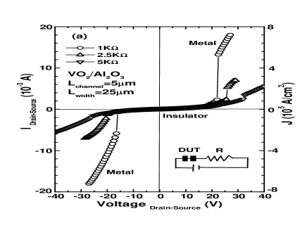
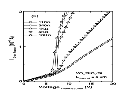
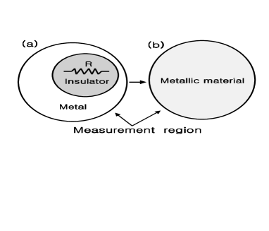
Figures 3 (a) and (b) show the external resistance dependence of the magnitude of abrupt current jumps observed at device II fabricated on a VO2/Al2O3 film II and device III fabricated on a VO2/SiO2/Si film III, respectively. With increasing external resistance, the magnitude of the abrupt current jump decreases and the MIT voltage increases. This can be explained by our model, as shown in Fig. 4 (a), where the metal region decreases with increasing external resistance in the measurement region. If only the metal region in Fig. 4 (a) is measured, the magnitude of the current jump might be of an order of 107 A/cm2, the current density of a good metal. That is, s observed at 5 K do not have the characteristics of a current jump, while, s measured at 1 K and less resistance, display jumps, as shown in Figs. 3(a) and (b). This indicates that the observed changes with an external resistance change, even though the intrinsic metal characteristic remain unchanged. Thus, the observed current density, , of an order of 105 A/cm2 in Fig. 3 (a) is an average of the metal region over the measurement region, as shown in Fig. 4 (b). The average is the effect of measurement. Furthermore, since the VO2 film has electrons and holes, as observed by Hall measurement in Fig. 1, it is regarded that the VO2 film is intrinsically inhomogeneous, although an external resistance effect is excluded. The inhomogeneity is an intrinsic characteristic of a material with an abrupt current jump and was confirmed by high resolution cross-sectional transmission-electron microscopy [12]. Thus, a true current jump cannot be measured in an inhomogeneous system, as shown in Fig. 4, as has been explained by the extended Brinkman-Rice picture [15].
We have observed a true dielectric breakdown which forms a current path with a very low source-drain voltage (or field) and a high current such as a ’short’ phenomenon, after a device is applied to a very high current or electric field. After the dielectric breakdown occurs, the current jump is not observed. The dielectric breakdown is regarded as a device breakdown. The abrupt current jump is reproducible without degradation even in thousands of measurements, when an external resistance is attached in the circuit. The external resistance is a decisive key to controlling the abrupt MIT for application devices.
In conclusion, the temperature dependence of the abrupt MIT explains the mechanism of the abrupt Mott MIT. In particular, the external resistance dependence of the magnitude of the current jump is an important key to application of the abrupt MIT to optic and electronic devices. Furthermore, the breakdown phenomenon observed in thin gate insulators [10, 11] may be the abrupt Mott MIT.
REFERENCES
- [1] G. Stefanovich, A. Pergament, and D. Stefanovich, J. Phys.: Condens. Matter 12, 8837 (2000).
- [2] F. Chudnovskiy, S. Luryi, B. Spivak, ”Future Trends in Microelectronics: the Nano Millennium”, (Ed. S. Luryi, J. M. Xu, A. Zaslavsky, Wiley Interscience Pub., 2002) p. 145.
- [3] H. T. Kim, B. G. Chae, D. H. Youn, S. L. Maeng, K. Y. Kang, http://xxx.lanl.gov/abs/cond-mat/0305632.
- [4] J. F. Natale, P. D. Hood, and A. B. Harker, J. Appl. Phys. 66, 5844 (1989).
- [5] M. Borek, F. Qian, V. Nagabushnam and R. K. Singh, Appl. Phys. Lett. 63, 3288 (1993).
- [6] Y. Muraoka and Z. Hiroi, Appl. Phys. Lett. 80 (2002) 583.
- [7] H. T. Kim, B. G. Chae, D. H. Youn, S. L. Maeng, G. O. Kim, K. Y. Kang, and Y. S. Lim, http://xxx.lanl.gov/abs/cond-mat/0308042.
- [8] Y. S. Lim, H. T. Kim, B. G. Chae, D. H. Youn, K. Y. Kang, S. J. Lee, K. Kim, unpublished.
- [9] N. F. Mott, in Metal-Insulator Transition (Taylor and Frances, 1990).
- [10] G. S. Bhalla, X. Du, and A. F. Hebard, Appl. Phys. Lett. 83 (2003) 2417.
- [11] H. K. Park, H. D. Yang, H. J. Sim, and H. S. Hwang, Extended Abstracts of the 2003 Int. Conf. on Solid State Devices and Materials, Tokyo 2003, p. 62.
- [12] D. H. Youn, J. W. Lee, B. G. Chae, H. T. Kim, S. L. Maeng, and K. Y. Kang, to be published in J. Appl. Phys..
- [13] F. J. Morin, Phys. Rev. Lett. 3, 34 (1959).
- [14] D. B. McWhan, T. M. Rice, and J. P. Remeika, Phys. Rev. Lett. 23, 1384 (1969).
- [15] H. T. Kim, in New Trends in Superconductivity (Kluwer, 2002);in NATO Science Series, VOl. II/67, 137 (2002); cond-mat/0110112.