Conduction in Carbon Nanotubes Through Metastable Resonant States
Abstract
We report here on electrical measurements on individual multi-walled carbon nanotubes (MWNTs) that show that the presence or movement of impurities or defects in the carbon nanotube can radically change its low temperature transport characteristics. The low temperature conductance can either decrease monotonically with decreasing temperature, or show a sudden increase at very low temperatures, sometimes in the same sample at different times. This unusual behavior of the temperature dependence of the conductance is correlated with large variations in the differential conductance as a function of the dc voltage across the wire. The effect is well described as arising from quantum interference of conduction channels corresponding to direct transmission through the nanotube and resonant transmission through a discrete electron state, the so-called Fano resonance.
pacs:
73.63.Fg, 85.35.Kt, 73.20.HbThere is tremendous interest in the transport properties of carbon nanotubes due to their potential for use in future nanodevices nextgeneration , and from their role as canonical models of one-dimensional electron transport luttinger . While individual single-walled carbon nanotubes are expected to show either semiconducting or metallic behavior depending on their chirality physicalproperties , the presence of impurities, defects and interactions is expected to modify this behavior backscattering ; defects . However, measuring the intrinsic transport properties of single or multiwalled carbon nanotubes is complicated by the experimental problem of making electrical contact to the nanotube. Quite often, the contact resistance between the metallic electrodes and nanotube is much higher than the resistance of the nanotube itself, so that the transport properties of the device are determined in large part by the properties of the metal-nanotube contacts. In spite of this problem, transport measurements on high contact-resistance carbon nanotube devices by a number of groups have elucidated the wide variety of physical problems that can be studied in these systems, including the Coulomb blockade set , the Kondo effect kondo , and Luttinger liquids luttinger .
In devices with lower contact resistances, the intrinsic properties of carbon nanotubes can be directly measured. For example, by using different techniques to obtain low resistance contacts, observation of quantization of the conductance in ballistic carbon nanotubes has been reported ballistic , and there are also suggestions of superconductivity in nanotube rope devices made with low resistance contacts superconductivity . However, much interesting physics still remains to be explored. In this Letter, we report on transport measurements on multiwalled carbon nanotubes (MWNTs) with low resistance contacts. The low-temperature differential conductance of these devices as a function of the dc voltage bias across them is highly asymmetric, showing large, reproducible fluctuations that can be as large as 10% of the total conductance. This conductance ‘fingerprint’ can change on thermal cycling to just 2 K, indicating that it might be associated with metastable impurities or mechanical instabilities. The fluctuations in are reflected in the zero-bias (=0) conductance as a function of temperature , which can either decrease or increase with decreasing temperatures at low temperatures, sometimes showing both dependences in a single sample upon thermal cycling. The sharp structure in can be described as arising from Fano resonances through resonant states in the device. The position of these peaks and dips frequently change on thermal cycling, indicating that the resonant states may arise from metastable impurities or defects in the device.

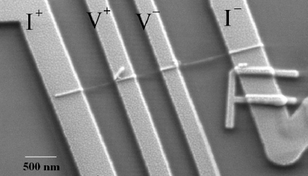
Our devices consist of an isolated MWCNT with four Au/Ti electrodes (Fig. 1). The arc-grown MWNTs, typically 2-5 m long and 25-50 nm wide, were spun onto an oxidized Si substrate from a suspension in dimethylformamide. After locating the nanotubes with respect to fiducial marks, and patterning electrodes by electron-beam lithography, thin film electrodes (5 nm Ti/50 nm Au) were deposited to make contact to the nanotube. Prior to deposition, a short-time oxygen plasma etch was used to improve the metal-nanotube contact resistance. Without this cleaning, the contact resistances were typically in the range of a few k to a few M, while this process reduced the contact resistance to a few hundred ohms. The presence of four electrodes enables us to make four-terminal resistance measurements on the MWCNTs, eliminating effects of the contact resistance between the MWCNT and the electrodes. In some devices, two external contacts were made to each electrode, as shown in Fig. 1, enabling direct measurements of the electrode-nanotube contact resistance; in the other devices, the contact resistance was inferred from differences between four-terminal and two-terminal measurements. The typical distance between the voltage probes was 300 nm. The samples were measured in a 3He refrigerator and a dilution refrigerator. A home-made ac resistance bridge was used to measure the four-terminal differential resistance as a function dc current using the probe configuration shown in Fig. 1, with ac excitation in the range of 0.25-1 nA to avoid heating effects. In this paper, we shall plot our measurements in terms of the differential conductance =1/() as a function of the dc voltage , obtained by numerically integrating the measured vs curves.

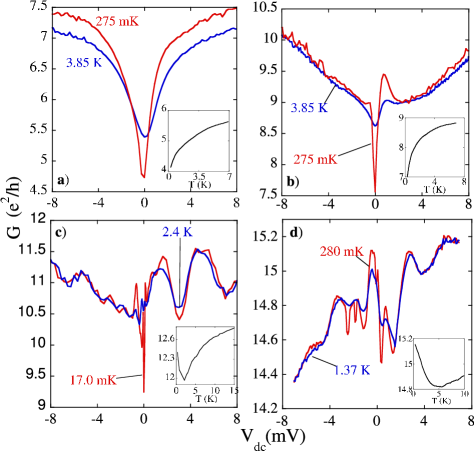
Figure 2 shows for four different samples with contact resistances ranging from 1 k to less than 100 , at two different temperatures each, and demonstrates the sample-specific behavior that can be seen in our devices. is highly asymmetric and shows large fluctuations, with the pattern of the fluctuations being different for different devices. In general, the structure in becomes sharper as the temperature is lowered: the peaks increase in conductance, while the valleys decrease in conductance. This gives rise to characteristically different temperature dependences for nominally identical samples: for example, if a peak is observed at =0, will increase with decreasing temperature, while if a valley is observed, it will decrease. (Of course, it is not necessary that either a peak or a valley occur at ). This is demonstrated in the insets to the panels in Fig. 2, which show the corresponding for each device. As demonstrated in Fig. 2, the structure in appears to increase on average as the resistance of the contacts decreases. Indeed, large fluctuations in are not seen in our samples with contact resistances in the k to M range; one sees instead a largely symmetric curve with reduced conductance near =0, and correspondingly, a monotonically decreasing .

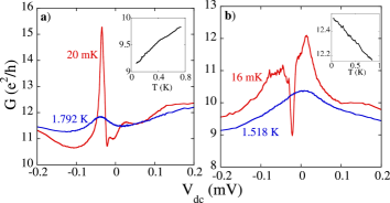
varies not only from sample to sample, but can also change in a single sample as a function of thermal cycling. Figures 3(a) and 3(b) show for Sample 3 (see the caption of Fig. 2), for two different cooldowns of the dilution refrigerator. As can be seen, there is a radical change after warming to room temperature: while the most prominent feature at low temperature in Fig. 3(a) is a peak, this feature has changed into a dip in Fig. 3(b). As we noted before, this change is also reflected in , as shown in the inset to the panels in Fig. 3. Indeed, we found that it was not necessary to warm the samples all the way to room temperature; warming to temperatures on the order of a few Kelvin changed the behavior of the sample, although the change was not as dramatic as shown in Figs. 3(a) and 3(b).
Sample-specific fluctuations of the conductance are well known in mesoscopic systems. In the case of disordered metals and semiconductors, they are associated with quantum interference of electron waves that are scattered by impurities, defects or grain boundaries in the sample ucf . Each scattering event introduces a finite but time-independent shift in the phase of the electron. The phases and phase shifts of the electrons can be modulated by external parameters such as a gate voltage or magnetic field. So long as time-dependent scattering processes that destroy the phase of the electron (processes such as electron-electron or electron-phonon scattering) are negligible, the interference of electrons manifests itself as aperiodic or periodic fluctuations of the conductance as a function of the external parameter ucfexp . Furthermore, since scattering from each impurity or defect introduces a phase shift, the movement of the impurity by even a very small distance (equivalent to 1/, where is the Fermi wave vector) will change the phase shift, resulting in a corresponding change in the conductance pattern noise . Time-dependent conductance changes have been observed in disordered metals, and this mechanism has been shown to be a source of noise in metals at low temperatures noiseexp .
A similar interference mechanism can also exist in relatively clean carbon nanotubes with one or a few number of impurities or defects. In this case, the interference can be between electron waves that are directly transmitted, and those that are transmitted via a resonant state. This interference between directly transmitted channels and resonant channels gives rise to a Fano resonance, well known in atomic scattering Fano . For simplicity, we consider the case of a single directly transmitted channel and a single resonant state. Transmission through the resonant channel is described by an amplitude Clerk . Without the factor , this gives the usual expression for resonant transmission through a localized state of energy (measured with respect to the Fermi energy ) and intrinsic energy width , , with a transmission of on resonance (). The transmission amplitude of the direct channel does not depend on , and can be described by an expression of the form , where is the transmission of the direct channel, and describes the phase difference between the direct and resonant path. The interference between the two paths is taken into account by taking the sum of the transmission amplitudes to calculate the total transmission coefficient, . The resulting conductance can be expressed in the Fano form
| (1) |
where is the complex Fano parameter Clerk . Note that far from resonance (), the conductance reduces to .
A number of characteristics distinguish the resulting Fano resonance from other resonances that might occur in carbon nanotubes. First, depending on the phase difference between the resonant and non-resonant transmission channels, the Fano resonance can give rise to a peak or dip in the conductance (or something in between). Second, the Fano lineshape can be asymmetric about the transmission maximum or minimum. Finally, the position of the resonance is determined by the energy of the resonant state, and does not necessarily occur at the Fermi energy (zero bias). These distinguishing characteristics, which can be clearly seen in our data, rule out other possible mechanisms (such as the Kondo effect kondo ) for the structure we observe in the differential resistance of our devices.
Two groups have recently reported observing Fano resonances in carbon nanotube devices. Kim et al. Kim measured the conductance of crossed MWNTs, and observed a Fano resonance in two of the devices. Noting that a Fano resonance was never observed in devices without crossed MWNTs, they associated the presence of the Fano resonance with the MWNT cross, although the mechanism by which a discrete electron level is created was not discussed. Yi et al. Yi measured the conductance of crosses consisting of metal electrodes patterned across MWNT bundles. In two of these devices, they observed non-monotonic behavior of the conductance near zero voltage bias, which they ascribed to a Fano resonance arising from interference between a Kondo resonance and non-resonant channels. However, the nature of the localized state giving rise to the Kondo resonance was not made clear. Furthermore, this interpretation is suspect in our opinion, because a Kondo resonance typically arises at the Fermi energy, and the resonances observed by Yi et al. were typically observed at voltage biases of 0.3-0.6 mV. In both papers, the metastable behavior we observe was not reported.

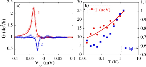
Fig. 4(a) shows the measured Fano resonances for the lower temperatures shown in Figs. 3(a) and 3(b), along with fits to the Fano function given above. To obtain these curves, the background conductance outside the region = [-0.1 mV,-0.02 mV] for curve 1, and = [-0.05 mV, 0.02 mV] for curve 2 has been fit, and subtracted from the experimental data. After subtraction, the conductance far from resonance would be 0. However, we arbitrarily introduce an offset of , corresponding to the conductance of two channels of a single-walled nanotube that coherently interfere with the resonant state, with the assumption that other channels that contribute to the background do not interfere with the resonant state. It can be seen that data are well described by the Fano equation. For curve 1, is in phase with on resonance, resulting in a maximum of conductance, while for curve 2, is out of phase with on resonance, resulting in a minimum of conductance. This change in the phase of the non-resonant channel and the resonant channel is a result of the annealing process, which presumably causes a change in the position of the impurity or defect that gives rise to the resonant state.
Fig. 4(b) shows the fitted value of and as a function of temperature for the conductance dip shown in Fig. 4(a). Both and increase with increasing temperature. Although the values we obtain for are comparable to those obtained by Kim et al., the temperature dependence is different. Kim et al. observed a linear temperature dependence, which they ascribed to thermal broadening of the linewidth, even though was less than . Our temperature dependence is not linear, which is not surprising, since we are in the regime . Fitting to a power law gives a dependence , shown as the solid line in Fig. 4(b); the origin of this power law is not clear to us. In contrast, while also increases with temperature at higher temperatures, it appears to saturate below 100 mK. The phase of remains essentially constant over the fitted temperature range.
What is the possible origin of the resonant states in our samples? Although we are not certain, the metastability we observe suggests impurities or structural defects cause variations in the potential seen by the electrons in the nanotube, which in turn lead to localized electronic states with well-defined resonant energies. Movement of the impurities or defects can give rise changes in the conductance through interference effects. Although the changes we observed in our samples typically occurred on the scale of days at low temperatures, we have also observed changes on the scale of hours. If there are many such impurities moving on a sufficiently rapid time scale, this may be one mechanism for the large noise in carbon nanotubes reported by some groups tubenoise .
Acknowledgements.
We thank the group of R. P. H. Chang for providing us the nanotubes used in these experiments, and D. E. Prober for a critical reading of the manuscript. Funding for this work was provided by a NASA/MSFC Phase II SBIR, Contract No. NAS8-02102, through a subcontract from Lytec, LLC.References
- (1) See e.g. S. Saito, Science 278, 77 (1997).
- (2) M. Bockrath et al., Nature 397, 598 (1999); Z. Yao et al., ibid. 402, 273 (1999).
- (3) R. Saito, G. Dresselhaus, and M.S. Dresselhaus, Physical Properties of Carbon Nanotubes (Imperial College, London, UK, 1998).
- (4) P.L. McEuen et al., Phys. Rev. Lett. 83, 5098 (1999), and references cited therein.
- (5) A. Bachtold et al., Nature 397, 673 (1999); C. Schönenberger et al., Appl. Phys. A 69, 283 (1999).
- (6) S.J. Tans et al., Nature 386, 474 (1997); M. Bockrath et al., Science 275, 1922 (1997).
- (7) J. Nygard, D.H. Cobden, and P.E. Lindelof, Nature 408, 342 (2000).
- (8) S. Frank et al., Science 280, 1744 (1998); J. Kong et al., Phys. Rev. Lett. 87, 106801 (2001).
- (9) M. Kociak et al., Phys. Rev. Lett. 86, 2416 (2001).
- (10) P.A. Lee and A.D. Stone, Phys. Rev. Lett. 55, 1622 (1985); P.A. Lee, A.D. Stone, and H. Fukuyama, Phys. Rev. B 35, 1039 (1987); B.L. Al’ tshuler, JETP Lett. 41, 648 (1985).
- (11) See, for example, S. Washburn and R.A. Webb, Adv. Phys. 35, 375 (1986), and references cited therein.
- (12) S. Feng, P.A. Lee, and A.D. Stone, Phys. Rev. Lett. 56, 1960 (1986).
- (13) N.O. Birge, B. Golding, and W.H. Haemmerle, Phys. Rev. B 42, 2735 (1990); B. Golding, N.M. Zimmerman, and S.N. Coppersmith, Phys. Rev. Lett. 68, 998 (1992).
- (14) U. Fano, Phys. Rev. 124, 1866 (1961).
- (15) For a good discussion of Fano resonances as applied to mesoscopic systems, see A.A. Clerk, X. Waintal, and P.W. Brouwer, Phys. Rev. Lett. 86, 4636 (2001).
- (16) J. Kim et al., Phys. Rev. Lett. 90, 166403 (2003).
- (17) W. Yi et al., Phys. Rev. Lett. 91, 076801 (2003).
- (18) P.G. Collins, M.S. Fuhrer, and A. Zettl, Appl. Phys. Lett. 76, 894 (2000); L. Roschier et al., ibid. 78, 3295 (2001); P.E. Roche et al., Eur. Phys. J. B 28, 217 (2002).