Differential Charge Sensing and Charge Delocalization
in a Tunable Double Quantum Dot
Abstract
We report measurements of a tunable double quantum dot, operating in the quantum regime, with integrated local charge sensors. The spatial resolution of the sensors allows the charge distribution within the double dot system to be resolved at fixed total charge. We use this readout scheme to investigate charge delocalization as a function of temperature and strength of tunnel coupling, demonstrating that local charge sensing can be used to accurately determine the interdot coupling in the absence of transport.
Coupled semiconductor quantum dots have proved a fertile ground for exploring quantum states of electron charge and spin. These “artifical molecules” are a scalable technology with possible applications in information processing, both as classical switching elements Chan02 ; Gardelis03 or as charge or spin qubits Engel03 . Charge-state superpositions may be probed using tunnel-coupled quantum dots, which provide a tunable two-level system whose two key parameters, the bare detuning and tunnel coupling between two electronic charge states vanderWiel03 , can be controlled electrically.
In this Letter, we investigate experimentally a quantum two-level system, realized as left/right charge states in a gate-defined GaAs double quantum dot, using local electrostatic sensing (see Fig. 1). In the absence of tunneling, the states of the two-level system are denoted and , where the pair of integers refers to the number of electrons on the left and right dots. For these two states, the total electron number is fixed, with a single excess charge moving from one dot to the other as a function of gate voltages. When the dots are tunnel coupled, the excess charge becomes delocalized and the right/left states hybridize into symmetric and antisymmetric states.
Local charge sensing is accomplished using integrated quantum point contacts (QPC’s) positioned at opposite sides of the double dot. We present a model for charge sensing in a tunnel-coupled two-level system, and find excellent agreement with experiment. The model allows the sensing signals to be calibrated using temperature dependence and measurements of various capacitances. For significant tunnel coupling, ( is electron temperature, is the single-particle level spacing of the individual dots), the tunnel coupling can be extracted quantitatively from the charge sensing signal, providing an improved method for measuring tunneling in quantum dot two-level systems compared to transport methods vanderWiel03 .
Charge sensing using a QPC was first demonstrated in Ref. Field93 , and has been used previously to investigate charge delocalization in a single dot strongly coupled to a lead in the classical regime Duncan99 , and as a means of placing bounds on decoherence in an isolated double quantum dot Gardelis03 . The back-action of a QPC sensor, leading to phase decoherence, has been investigated experimentally Buks98 and theoretically backaction . Charge sensing with sufficient spatial resolution to detect charge distributions within a double dot has been demonstrated in a metallic system Amlani97 ; Buehler03 . However, in metallic systems the interdot tunnel coupling cannot be tuned, making the crossover to charge delocalization difficult to investigate. Recently, high-bandwidth charge sensing using a metallic single-electron transistor Schoelkopf98 , allowing individual charging events to be counted, has been demonstrated Lu03 . Recent measurements of gate-defined few-electron GaAs double dots Elzerman03 have demonstrated dual-QPC charge sensing down to , but did not focus on sensing at fixed electron number, or on charge delocalization. The present experiment uses larger dots, containing electrons each (though still with temperature less than level spacing, see below).
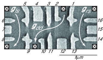
The device we investigate, a double quantum dot with adjacent charge sensors, is formed by sixteen electrostatic gates on the surface of a GaAs/Al0.3Ga0.7As heterostructure grown by molecular beam epitaxy (see Fig. 1). The two-dimensional electron gas layer, 100 nm below the surface, has an electron density of and mobility . Gates 3/11 control the interdot tunnel coupling while gates 1/2 and 9/10 control coupling to electron reservoirs. In this measurement, the left and right sensors were QPCs defined by gates 8/9 and 13/14, respectively; gates 6, 7, 15, and 16 were not energized. Gaps between gates 5/9 and 1/13 were fully depleted, allowing only capacitive coupling between the double dot and the sensors.
Series conductance, , through the double dot was measured using standard lock-in techniques with a voltage bias of at 87 . Simultaneously, conductances through the left and right QPC sensors, and , were measured in a current bias configuration using separate lock-in amplifiers with excitation at 137 and 187 . Throughout the experiment, QPC sensor conductances were set to values in the 0.1 to 0.4 range by adjusting the voltage on gates 8 and 14.
The device was cooled in a dilution refrigerator with base temperature . Electron temperature at base was , measured using Coulomb blockade peak widths with a single dot formed. Single-particle level spacing for the individual dots was also measured in a single-dot configuration using differential conductance measurements at finite drain-source bias. Single-dot charging energies, for both dots (giving dot capacitances ), were extracted from the height in bias of Coulomb blockade diamonds LK97 .
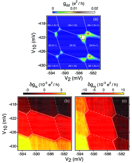
Figure 2(a) shows as a function of gate voltages and , exhibiting the familiar ‘honeycomb’ pattern of series conductance through tunnel-coupled quantum dots Pothier92 ; Blick96 ; Livermore96 . Conductance peaks at the honeycomb vertices, the so-called triple points, result from simultaneous alignment of energy levels in the two dots with the chemical potential of the leads. Although conductance can be finite along the honeycomb edges as a result of cotunneling, here it is suppressed by keeping the dots weakly coupled to the leads. Inside a honeycomb, electron number in each dot is well defined as a result of Coulomb blockade. Increasing () at fixed () raises the electron number in the left (right) dot one by one.
Figures 2(b) and 2(c) show left and right QPC sensor signals measured simultaneously with . The sensor data plotted are , the left (right) QPC conductances after subtracting a best-fit plane (fit to the central hexagon) to remove the background slope due to cross-coupling of the plunger gates (gates 2 and 10) to the QPCs. The left sensor shows conductance steps of size along the (more horizontal) honeycomb edges where the electron number on the left dot changes by one (solid lines in Fig. 2(b)); the right sensor shows conductance steps of size along the (more vertical) honeycomb edges where the electron number of the right dot changes by one (solid lines in Fig. 2(c)). Both detectors show a conductance step, one upward and the other downward, along the -degree diagonal segments connecting nearest triple points. It is along this shorter segment that the total electron number is fixed; crossing the line marks the transition from to . Overall, we see that the transfer of one electron between one dot and the leads is detected principally by the sensor nearest to that dot, while the transfer of one electron between the dots is detected by both sensors, as an upward step in one and a downward step in the other, as expected.
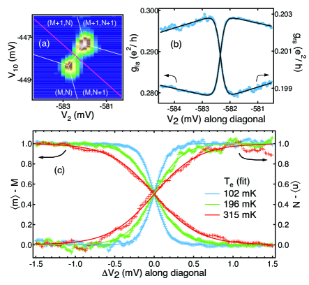
Focusing on interdot transitions at fixed total charge, i.e., transitions from to , we present charge-sensing data taken along the “detuning” diagonal by controlling gates and , shown as a red diagonal line between the triple points in Fig. 3(a). Raw data (no background subtracted) for the two sensors are shown in Fig. 3(b). The transfer of the excess charge from left dot to right dot causes conductance steps on both QPCs, clearly discernable from background slopes caused by coupling of gates 2 and 10 to the QPCs.
Also shown in Fig. 3(b) are fits to the raw sensor data based on a model of local sensing of an isolated two-level system in thermal equilibrium, which we now describe. Varying and along the red diagonal changes the electrostatic energy difference, or bare detuning , between and states. The lever arm relating gate voltage to detuning is set by the slope of the diagonal cut (see Fig. 3(a)) and various dot capacitances, and can be calibrated experimentally as described below. When the tunnel coupling mixing these two states is small compared to the single-particle level spacings for the individual dots, we can consider a two-level system whose ground and excited states, separated by an energy , consist of superpositions of and Cohen96 . The probability of finding the excess charge on the left dot while in the ground (excited) state is . The excited state is populated at finite temperature, with an average occupation . The average excess charge (in units of ) on the left and right dots is thus:
| (1) |
Our model assumes that each sensor responds linearly to the average excess charge on each dot, but more sensitively to that on the nearest dot as demonstrated experimentally in Fig. 2. The resulting model for sensor conductance is:
| (2) |
The first term on the right is the background conductance of the QPC, the second term represents the linear response to average excess charge, and the third represents direct coupling of the swept gates to the QPC. As shown in Fig. 3(b), our model gives very good fits to the data. For each trace (left and right sensors), fit parameters are , , , and . In these data, the tunnel coupling is weak, and we may set .
Figure 3(c) shows the effect of increasing electron temperature on the transition width. Here, vertical axes show excess charge extracted from fits to QPC sensor conductance data. Sweeps along the red diagonal were taken at refrigerator temperatures of (blue), (green) and (red). We use the (red) data to extract the lever arm relating voltage along the red diagonal (see Fig. 3(a)) to detuning . At this temperature, electrons are well thermalized to the refrigerator, and thus . The width of the sensing transition at this highest temperature lets us extract the lever arm, which we then use to estimate the electron temperature for the blue (green) data, getting .
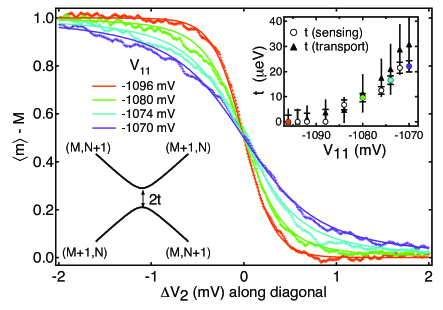
We next investigate the dependence of the sensing transition on interdot tunneling in the regime of strong tunneling, . Figure 4 shows the left QPC sensing signal, again in units of excess charge, along the detuning diagonal crossing a different pair of triple points, at base temperature and for various voltages on the coupling gate 11. For the weakest interdot tunneling shown ( mV), the transition was thermally broadened, i.e., consistent with in Eqs. (1) and (2), and did not become narrower when was made more negative. On the other hand, when was made less negative, the transition widened as the tunneling between dots increased. Taking for all data in Fig. 4 and calibrating voltage along the detuning diagonal by setting for the mV trace allows tunnel couplings to be extracted from fits to our model of the other tunnel-broadened traces. We find (green trace), (turquoise trace), and (purple trace). Again, fits to the two-level model are quite good, as seen in Fig. 4.
Finally, we compare tunnel coupling values extracted from charge sensing to values found using a transport-based method that takes advantage of the dependence of the splitting of triple points (honeycomb vertices) Ziegler00 ; vanderWiel03 . In the weak tunneling regime, , the splitting of triple points along the line separating isocharge regions and has two components in the plane of gate voltages, denoted here and . The lower and upper triple points are found where the lowest energy state (the delocalized antisymmetric state) becomes degenerate with the charge states and , respectively. Using the electrostatic model in Ref. vanderWiel03 , we can show that are related to various dot capacitances and by
| (3) |
Here, is the capacitance from gate to the left (right) dot, is the self-capacitance of each dot, and is the interdot mutual capacitance. All these capacitances must be known to allow extraction of from . Gate capacitances are estimated from honeycomb periods along respective gate voltage axes, . Self-capacitances can be obtained from double dot transport measurements at finite bias vanderWiel03 . However, lacking that data, we estimate from single-dot measurements of Coulomb diamonds LK97 . Mutual capacitance is extracted from the dimensionless splitting , measured at the lowest tunnel coupling setting.
Tunnel coupling values as a function of voltage on gate 11, extracted both from charge sensing and triple-point separation, are compared in the inset of Fig. 4. The two approaches are in good agreement, with the charge-sensing approach giving significantly smaller uncertainty for . The two main sources of error in the sensing approach are uncertainty in the fits (dominant at low ) and uncertainty in the lever arm due to a conservative 10 percent uncertainty in at base. Error bars in the transport method are set by the smearing and deformation of triple points as a result of finite interdot coupling and cotunneling. We note that besides being more sensitive, the charge-sensing method for measuring works when the double dot is fully decoupled from its leads. Like the transport method, however, the sensing approach assumes (which may not be amply satisfied for the highest values of ).
In conclusion, we have demonstrated differential charge sensing in a double quantum dot using paired quantum point contact charge sensors. States and , with fixed total charge, are readily resolved by the sensors, and serve as a two-level system with a splitting of left/right states controlled by gate-defined tunneling. A model of local charge sensing of a thermally occupied two-level system agrees well with the data. Finally, the width of the transition measured with this sensing technique can be used to extract the tunnel coupling with high accuracy in the range .
We thank M. Lukin, B. Halperin and W. van der Wiel for discussions, and N. Craig for experimental assistance. We acknowledge support by the ARO under DAAD55-98-1-0270 and DAAD19-02-1-0070, DARPA under the QuIST program, the NSF under DMR-0072777 and the Harvard NSEC, Lucent Technologies (HJL), and the Hertz Foundation (LIC).
References
- (1) I.H. Chan et al., Appl. Phys. Lett. 80, 1818 (2002).
- (2) S. Gardelis et al., Phys. Rev. B 67, 073302 (2003).
- (3) H.-A. Engel et al., arXiv:cond-mat/0309023 (2003).
- (4) W.G. van der Wiel et al., Rev. Mod. Phys. 75, 1 (2003).
- (5) M. Field et al., Phys. Rev. Lett. 70, 1311 (1993).
- (6) D.S. Duncan et al., Appl. Phys. Lett. 74, 1045 (1999).
- (7) E. Buks et al., Nature 391, 871 (1998).
- (8) I. L. Aleiner, N. S. Wingreen, Y. Meir, Phys. Rev. Lett. 79, 3740 (1997); Y. Levinson, Europhys. Lett. 39, 299 (1997).
- (9) R.J. Schoelkopf et al., Science 280, 1238 (1998).
- (10) Wei Lu et al., Nature 423, 422 (2003).
- (11) J.M. Elzerman et al., Phys. Rev. B 67, R161308 (2003).
- (12) I. Amlani et al., Appl. Phys. Lett. 71, 1730 (1997).
- (13) T.M. Buehler et al., Appl. Phys. Lett. 82, 577 (2003).
- (14) L.P. Kouwenhoven et al., in Mesoscopic Electron Transport, edited by L.L. Sohn, L.P. Kouwenhoven, and G. Schön (Kluwer, Dordrecht, 1997).
- (15) H. Pothier et al., Europhys. Lett. 17, 249 (1992).
- (16) R.H. Blick et al., Phys. Rev. B 53, 7899 (1996).
- (17) C. Livermore et al., Science 274, 5291 (1996).
- (18) For a useful review of two-level systems, see C. Cohen-Tannoudji et al., Quantum Mechanics, Vol. 1, Ch. 4, (Wiley, New York, 1977).
- (19) R. Ziegler et al., Phys. Rev. B 62, 1961 (2000)