Dimensionality effects on non-equilibrium electronic transport in Cu nanobridges
Abstract
We report on non-equilibrium electronic transport through normal-metal (Cu) nanobridges coupled to large reservoirs at low temperatures. We observe a logarithmic temperature dependence of the zero-bias conductance, as well as a universal scaling behavior of the differential conductance. Our results are explained by electron-electron interactions in diffusive metals in the zero-dimensional limit.
pacs:
In clean bulk metals, the electron-electron interaction, although strong, is screened sufficiently to make an independent electron picture valid for a broad range of materials. In disordered metals, however, screening is limited by the diffusive motion of electrons, leading to a well-known correction to the linear conductance and to the one-particle density of states (DOS) near the Fermi level Altshuler and Aronov (1985). The corrections depend on dimensionality, and for the DOS are proportional to , and in three, two and one dimensions, respectively, where is the energy difference to the Fermi level, and logarithmic corrections to leading power laws have been omitted. The DOS correction is spectroscopically resolved as a zero-bias anomaly (ZBA) in tunneling experiments. For metallic point contacts, the occurrence of ZBAs has been reported in the literature for a long time Yanson and Shklyarevskii (1986); Ralph et al. (1994); Anaya et al. (2003); Yu and Natelson (2003), and attributed to various physical mechanisms like Kondo scattering by magnetic impurities, two-channel Kondo scattering by two-level systems, or Coulomb interaction.
In our previous work Weber et al. (2001), we have presented transport measurements on thin, short metallic films connected to large reservoirs. In these films, all inelastic scattering lengths were much larger than the sample size, such that a well-defined non-equilibrium distribution function with a double-step Pothier et al. (1997) in the electronic system can be assumed. The elastic mean free path was of the order of the film thickness, while the lateral dimensions of the films were much larger, i.e. the diffusive random-walk of the electrons is essentially two-dimensional (2D). We observed a logarithmic temperature dependence of the linear conductance, and a ZBA in the differential conductance which obeyed a parameter-free scaling relation with a logarithmic energy dependence. From a careful analysis of the energy and magnetic-field dependence and the reproducible amplitude of the ZBA, independent of sample preparation, we ruled out an explanation based on Kondo or two-channel Kondo physics for the anomaly observed in our samples. Our results were explained theoretically based on the Aharonov-Altshuler corrections in two dimensions extended to the non-equilibrium situation in a finite-size sample. Recently, further theoretical work on Coulomb interaction in non-equilibrium transport of metallic nanobridges Golubev and Zaikin (2001) has been reported. A logarithmic correction to the conductance, and a scaling form indistinguishable from our results, is predicted. These results are found to be independent of microscopic details, as long as the sample is fully phase coherent. Especially, the predictions are not specific to a two-dimensional thin film sample. We have therefore extended our investigation to clarify the dependence of the logarithmic ZBA on dimensionality by changing the sample geometry.
| sample | ||||||
|---|---|---|---|---|---|---|
| Cu1 | 31.7 | 12.4 | 5.3 | 20.9 | 3.9 | |
| Cu2 | 16.7 | 10.4 | 6.3 | 24.8 | 6.1 |
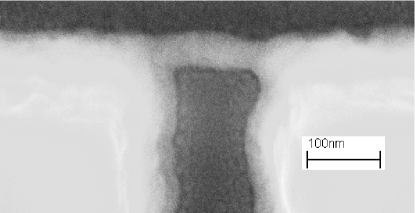
The samples presented in this study were prepared by e-beam lithography and shadow-evaporation techniques. A silicon wafer with 600 nm of thermal oxide was coated with two layers of e-beam resist, with the lower layer being PMMA/MAA and the upper layer PMMA 950K. Then, a mask with large areas for the reservoirs and a thin slit for the bridge was defined by e-beam lithography. 250 nm of Cu was evaporated under an angle of through the mask, forming the reservoirs, contact leads and a shadow of the bridge unconnected to the rest of the structure. Then, the bridge was evaporated under an angle of through the mask, closing the gap between the reservoirs. Here, the thick Cu layer on top of the resist resulting from the first evaporation somewhat narrows the slit left for the bridge, allowing for bridges down to approximately 20 nm width. After lift-off the samples were quickly mounted into a dilution refrigerator. Total exposure time to air was kept to less than 30 minutes in order to minimize oxide formation. The zero-bias resistance was measured using an AC resistance bridge. Care was taken to keep the excitation amplitude below the thermal energy scale. For the differential resistance measurements, an additional DC current was applied. Measurements were carried out at temperatures between 0.1 and 3 K and with magnetic fields of up to 12 T applied perpendicular to the substrate plane. We present data of two samples, Cu1 and Cu2, with parameters given in Table 1. The mean free path was obtained from , and the diffusion constant from Einstein’s relation , where is the resistivity of the bridge, and the density of states at the Fermi level. The material parameters were taken from Ashcroft and Mermin (1976). From , the Thouless energy was calculated.
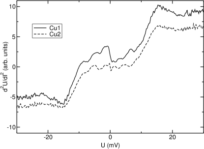
To check whether the measurements indeed establish a well-defined non-equilibrium with negligible inelastic scattering, differential resistance measurements were carried out to bias voltages up to 30 mV in order to observe point contact spectra. These high-bias data are plotted in Fig. 2 as vs. . The data clearly exhibit peaks at , followed by a broad shoulder. These peaks can be related to backscattering by optical phonons in the reservoirs, and are consistent with published results for copper point contacts in the diffusive regime Yanson and Shklyarevskii (1986). The observation of well-resolved point contact spectra at bias voltages an order of magnitude beyond the regime of the ZBA clearly shows that broadening of the energy distribution due to self-heating is small. Independently, we have estimated the effective temperature due to self-heating in a model similar to that presented in Ref. Henny et al. (1999), and found a negligible temperature rise compared to the bias voltage.
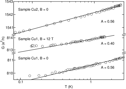
In Fig. 3, the temperature dependence of the zero-bias conductance of the two samples is shown. Both display a logarithmic temperature dependence in a temperature range from 0.2 K to 1.2 K. The data can be fitted with
| (1) |
where is the conductance, the temperature and an arbitrary reference temperature. The amplitude in zero applied magnetic field is about 0.56 for both samples. For sample Cu1, measurements were performed in a magnetic field , where the amplitude is reduced to 0.40 .
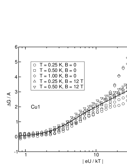
The scaling form
| (2) |
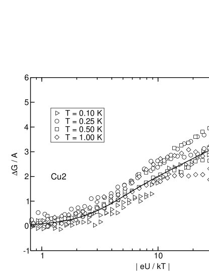
is employed to describe our data Weber et al. (2001). Here, is the applied voltage, the Boltzmann constant, and is a universal function. This formula suggests rescaling and plotting the data as vs. . Such scaling plots of the data for samples Cu1 and Cu2 are shown in Figs. 4 and 5. As can be seen, the data of both samples collapse onto a common function in the low bias regime, whereas for larger bias, deviations with a reproducible dependence on instead of are observed. The onset of these deviations is consistent with our estimate of the Thouless energy. These deviations are presumably voltage-dependent universal conductance fluctuations (VUCF), and can also be seen as small wiggles in the point contact spectra in Fig. 2, where the ZBA itself is resolved as a steep negative slope around zero bias.
The universal scaling function has been calculated by means of a tunneling Hamiltonian, which couples the interacting diffusive metal to ideal leads Weber et al. (2001). As the bridge is shorter than all inelastic scattering length scales, the bias voltage is expected to create a non-equilibrium double-step distribution function in the electronic system, leading to a spectroscopic resolution of interaction corrections to the density of states. It was shown that the dependence of two-dimensional films is effectively cut off to a simple dependence, as only the lowest lying diffusion mode is relevant for our finite-length samples as long as energies below the Thouless energy are considered. A similar treatment Schwab and Raimondi (2002) confirms this result, and predicts the amplitude of the anomaly to be in the range , depending on the transparency of the bridge-to-lead interface.
An alternative treatment of the ZBA in a coherent conductor in series with an environmental impedance has been given by Golubev et al. Golubev and Zaikin (2001) and Yeyati et al. Yeyati et al. (2001). In this case, the ZBA is interpreted as a residue of the well known Coulomb blockade in the limit of high transparency. The theory does not depend on microscopic details or the extent of the conductor, as long as it is phase-coherent. A logarithmic temperature dependence is predicted, along with a scaling function that is numerically indistinguishable from (2) Golubev and Zaikin (2001). The amplitude is predicted to be 2/3 for a diffusive conductor, in which case the resistance of the conductor itself serves as the environmental impedance.
For our present study, we deliberately varied the dimensionality of the diffusive motion compared to our previous work: Width, height and mean free path are approximately equal, thus the nanobridges are now short wires (1D) instead of films (2D). Nonetheless, the logarithmic temperature dependence and scaling behavior calculated for the short films is observed, with an amplitude in agreement with the range of the predicted values Golubev and Zaikin (2001); Schwab and Raimondi (2002). We find that the scaling behavior is valid in the bias voltage range defined by the Thouless energy. We therefore conclude that the lateral dimensions of the sample compared to the mean free path, and therefore the dimensionality of the diffusive motion, are irrelevant, as long as , and only the lowest lying diffusion mode is realized. Thus, even though it employs a film or wire geometry, our experiment effectively constitutes the zero-dimensional limit of electron-electron interaction. This fact has been pointed out by a theoretical treatment similar to our previous work Schwab and Raimondi (2002). The consistency with the results of Golubev et al. Golubev and Zaikin (2001) demonstrates the close relationship between the environmental Coulomb interaction and the electron-electron interaction in diffusive metals, which has recently been demonstrated in a tunneling experiment Pierre et al. (2001).
To conclude, we have presented transport measurements on short, phase-coherent metallic wires in a well-defined electronic non-equilibrium situation. We find the same logarithmic temperature dependence and scaling behavior as observed previously in short films. We therefore identify our results with electron-electron interactions in a diffusive metal in the zero-dimensional limit. Our experiment demonstrates the close relation between electron-electron interaction in diffusive metals and the environmental Coulomb interaction.
Acknowledgements.
Useful discussions with P. Schwab, J. Kroha and A. Zaikin are gratefully acknowledged, as well as the support of M. Brückel in the sample fabrication.References
- Altshuler and Aronov (1985) B. L. Altshuler and A. G. Aronov, in Electron-electron interactions in disordered systems, edited by A. L. Efros and M. Pollak (North-Holland Physics Publishers, 1985), p. 1.
- Yanson and Shklyarevskii (1986) I. K. Yanson and O. I. Shklyarevskii, Sov. J. Low. Temp. Phys. 12, 509 (1986).
- Ralph et al. (1994) D. C. Ralph, A. W. W. Ludwig, J. von Delft, and R. A. Buhrman, Phys. Rev. Lett. 72, 1064 (1994).
- Anaya et al. (2003) A. Anaya, A. L. Korotkov, M. Bowman, J. Wadell, and D. Davidovich, J. Appl. Phys. 93, 3501 (2003).
- Yu and Natelson (2003) L. H. Yu and D. Natelson, Appl. Phys. Lett. 82, 2332 (2003).
- Weber et al. (2001) H. B. Weber, R. Häussler, H. v. Löhneysen, and J. Kroha, Phys. Rev. B 63, 165426 (2001).
- Pothier et al. (1997) H. Pothier, S. Guéron, N. O. Birge, D. Estéve, and M. H. Devoret, Phys. Rev. Lett. 79, 3490 (1997).
- Golubev and Zaikin (2001) D. S. Golubev and A. D. Zaikin, Phys. Rev. Lett. 86, 4887 (2001).
- Ashcroft and Mermin (1976) N. W. Ashcroft and N. D. Mermin, Solid State Physics (W. B. Saunders Company, 1976).
- Henny et al. (1999) M. Henny, S. Oberholzer, C. Strunk, and C. Schönenberger, Phys. Rev. B 59, 2871 (1999).
- Schwab and Raimondi (2002) P. Schwab and R. Raimondi, Eur. Phys. J. B 30, 5 (2002).
- Yeyati et al. (2001) A. L. Yeyati, A. M. Rodero, D. Esteve, and C. Urbina, Phys. Rev. Lett. 87, 046802 (2001).
- Pierre et al. (2001) F. Pierre, H. Pothier, P. Joyez, N. O. Birge, D. Estéve, and M. H. Devoret, Phys. Rev. Lett. 86, 1590 (2001).