Opposite effects of NO2 on electrical injection
in porous silicon gas sensors
Abstract
The electrical conductance of porous silicon fabricated with heavily doped p-type silicon is very sensitive to NO2. A concentration of 10 ppb can be detected by monitoring the current injection at fixed voltage. However, we show that the sign of the injection variations depends on the porous layer thickness. If the thickness is sufficiently low – of the order of few µ m – the injection decreases instead of increasing. We discuss the effect in terms of an already proposed twofold action of NO2, according to which the free carrier density increases, and simultaneously the energy bands are bent at the porous silicon surface.
Porous silicon (PSi) is obtained by electrical anodization of crystalline silicon (Si) substrates Bisi et al. (2000). The internal surface versus volume ratio of PSi can reach several hundreds of m ^ 2 per c m ^ 3 , leading to strong dependence of optical and electrical properties of PSi on the environment. For this reason, PSi is an interesting material for gas sensors.
Recently, several reports have been focused on PSi sensors fabricated using heavily doped p-type Si (p+ PSi), in which the sensitive parameter is the electrical conductance Boarino et al. (2000); Baratto et al. (2001); Boarino et al. (2001); Timoshenko et al. (2001); Pancheri et al. (2003); Chiesa et al. (2003). In absence of gases, the electrical injection in sufficiently thick ( 30 µ m ) p+ PSi layers is very low. In fact, the anodization leads to a porous structure almost depleted of mobile charges, despite the concentration of boron dopants is essentially unchanged by the anodization, remaining approximately as high as in the starting p+ substrate ( c m -3) Polisski et al. (1998, 1999). The absence of mobile charges is ascribed to hole trapping Boarino et al. (2001), but the actual mechanism is still controversial Chiesa et al. (2003). In presence of specific gases, the mobile carrier population changes, usually leading to increases of conductance, as in the case of NO2 Boarino et al. (2000); Baratto et al. (2001); Boarino et al. (2001); Timoshenko et al. (2001); Pancheri et al. (2003); Chiesa et al. (2003) or NH3 Chiesa et al. (2003).
The presence of NO2 is reported to free the trapped holes at interface states Boarino et al. (2001); Timoshenko et al. (2001). As a consequence, the conductivity increases because of the increased free hole concentration Boarino et al. (2000); Baratto et al. (2001); Boarino et al. (2001); Timoshenko et al. (2001); Pancheri et al. (2003). The process is very effective for sensing: the presence of NO2 can be detected at concentrations as low as 12 ppb Pancheri et al. (2003), and 10 ppb, as shown below (Figure 1). NO2 is a product of internal combustion engines and causes lung diseases. Most of pollution regulations set the attention level of NO2 around 100 ppb (for example, Italian Ministerial Decree, April 15, 1994). Hence, the required level of sensitivity for realistic applications is achievable in p+ PSi.
The sensitivity to NO2 is affected by both sensor’s porosity Boarino et al. (2000) and micro structure Gaburro et al. (2003). In this work, we report a quite surprising effect: the electrical injection in p+ PSi in presence of NO2 can increase or decrease, depending on the thickness of the p+ PSi layer. The known effect – the increase in the electrical injection originated by the increase of conductance – has been reported in thick samples ( 30 µ m ) Boarino et al. (2000); Baratto et al. (2001); Boarino et al. (2001); Timoshenko et al. (2001); Pancheri et al. (2003). We report here for the first time the opposite behavior of thin samples ( 2 µ m ), in which the injection decreases in presence of NO2.
p+ PSi layers were grown by electrochemical dissolution in an HF-based solution on a single-crystalline p-type (100) heavily-doped Si substrate. Substrate nominal resistivity was 6-15 m Ω c m . Before the anodization, the native oxide was removed from the backside of the wafers, and aluminium back contacts were deposited by evaporation. In order to achieve high sensitivity to NO2, we have used as anodizing solution a mixture of 3 parts (in volume) of aqueous HF (48% wt.) and 7 parts of ethanol. The etching was performed by applying an etching current density of 50 m A / c m ^ 2 . We fabricated two types of samples. The first type (hereafter referred to as “thick”) was fabricated using an etching time of 1363 s , whereas the second type (“thin”) was obtained with an etching time of 127 s . Thus, thick and thin samples were fabricated with exactly the same procedure, except for the anodization time. After anodization, the samples were rinsed in ethanol and pentane, and dried in ambient air. Scanning Electron Microscopy (SEM) images showed a layer thickness of about 32 and 2 µ m , respectively, for thick and thin samples. From normal reflectance measurements, a refractive index of about 1.4 was calculated, and using Bruggeman approximation Bisi et al. (2000) we have estimated that porosity was about 78%.
Gold electrodes were deposited by evaporation on the PSi top surface. Copper wires were connected to the gold electrodes using an epoxy silver paste.
For the electrical characterization, the sensors were kept in a sealed chamber under controlled flux of gases coming from certified cylinders. Humid air was obtained by flowing dry air through a bubbler. Different relative humidity levels and NO2 concentrations were obtained mixing humid air, dry air and a dilute solution of NO2 in air (550 ppb) with a flow control system. Relative humidity was monitored using a calibrated hygrometer. In order to characterize the time response, a bias voltage of -1 V was applied on one of the top contacts with respect to the back contact, and the injected current was constantly monitored (Figure 1).
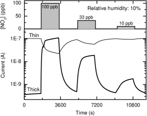
Although the injected current does not totally stabilize after 30 minutes, data of Figure 1 suggest that the most significant current variations are observed within such time period. Thus, I-V characterization, performed as a separate measurement, was acquired waiting an assumed 1800 s settling time after the gas switch. I-V characterizations are reported in Figure 2.

The main result discussed in this work is clearly visible in both Figures 1 and 2: in presence of NO2, the injected current increases in the thick sensor, and decreases in the thin one.
In the case of the thick sensor, the impedance of the device is dominated by the high resistance of the thick central layer. During the exposure to NO2, the conductance of the p+ PSi layer increases, as a consequence of the release of trapped holes, as already established Timoshenko et al. (2001); Boarino et al. (2001). Thus, the injection increases in presence of NO2. In Figure 2, the increase is visible by comparing the thick lines of plot a) and b). The I-V characteristic is symmetric with respect to a change of sign in the voltage.
The behavior of the thin sensor is harder to explain. The first observation is that in absence of NO2 the current injection is three orders of magnitude larger than in the thick sensor (Figure 2, plot a), even though the thickness is only one order of magnitude lower. This result suggests that in the thin sensor, the resistivity of the porous layer does not significantly limit the injection, which is therefore dominated by the behavior of the two junctions.
The value of the work function of gold is similar to the work function of p+ Si ( eV). Therefore, we assume that the two junctions behave similarly, in terms of the balance of excess charge at the junction regions. Since the p+ PSi is essentially an intrinsic semiconductor Polisski et al. (1998, 1999), the DC electrical behavior should be similar to the one of a quasi-symmetric p+-i-p+ device. Although this is clearly a rough simplification, nevertheless it seems a reasonable starting point, since the I-V characteristics of the thin sensor are not very asymmetric with respect to the voltage inversion (Figure 2).
A recent study on n+-i-n+ Si structures Cech (2000) has shown that, in structures with doping profiles similar to our thin sensor, when the distance between the junctions is in the range of 2 µ m or less, extra free carriers diffusing from the heavily doped regions accumulate over most of the intrinsic region. This result suggests that the hole density in the porous layer of our thin sensor is likely larger than the equilibrium density in bulk p+ PSi, because of the nearby junctions. In this sense, the two junctions are close to each other. Also, it is reasonable to assume that electron current density is negligible Cech (2000). Finally, Ref. Cech (2000) shows that in these structures the injection can increase if the density of defect states is rearranged in energy. We think that an energetic rearrangement at the surface is the only way to reconcile an increase of free carrier density with a decrease of the injected current, and to explain our experimental results with the thin sensor.
An interesting possibility is the detailed mechanism of reactivation of boron dopants by NO2 suggested by Boarino et al. Boarino et al. (2001): in p+ PSi, close the midgap energy, there is a high density of dangling bonds (). In absence of gases, ionization of boron dopants can involve such defect states (). The process does not produce free holes because of the trapping action of the defect states (). The Fermi level remains between the energy levels of boron and defect states, as schematized in Figure 3, (a).
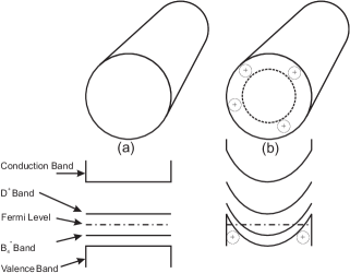
The presence of NO2 bends the energy bands upward at the PSi surface, pulling the Fermi level below the boron energy, and restoring the original doping action of boron (Figure 3,b) Boarino et al. (2001). An interesting feature of this model is the energetically favorable location of holes at the outer surface of conductive paths. In other words, the effect of NO2 can be envisioned as twofold: holes are de-trapped and pulled at the surface. The latter aspect can be pictured as a reduction of the effective conductive area (as in Figure 3, b) or more appropriately as a reduction of hole mobility, because of larger surface scattering. If the hole density is very low (as in the thick sensor), in absence of NO2 there is hardly any conduction. The hole repopulation induced by NO2 totally obscures any effect on mobility. On the contrary, if hole density is not negligible even in absence of NO2, a mobility reduction might be the only surviving effect of NO2. In the thin sensor, the hole density is higher than its equilibrium value because of diffusion from the junctions. The hole de-trapping by NO2 is giving negligible contribution to the overall hole density. Thus, we suppose that in thin sensors the only significant effect is the the band bending, which reduces the effective mobility, increasing the resistance.
If the bias is reversed, the situation is essentially the same, except that the role of the two junctions is exchanged. The slight asymmetry of I-V curves of thin sensors (Figure 2) is probably due to this material asymmetry.
Finally, we wish to emphasize that the observed effect explains why all the previous reports of p+ PSi were focused on thick sensors: it is not just a matter of increasing the sensitivity, but rather of obscuring the contrasting effect of mobility lowering, isolated here in thin sensors. In thick sensors, the injection is dominated by free carrier repopulation.
In conclusion, in thin porous silicon sensors (thickness of the order of few µ m or less), the carrier density is determined by the hole diffusion from the junctions. The surviving effect of NO2 in thin sensors is an effective narrowing of the conductive cross-sections, which in turn lowers the effective hole mobility. As a consequence, the net effect of NO2 in thick and thin porous silicon sensors is opposite in sign. For this reason, the gas sensing effects related to modulation of free carrier concentration are best exploited if the porous layer thickness is at least a few tens of µ m .
We acknowledge the support of INFM, progetto PAIS 2001 ”SMOG” and of Provincia Autonoma di Trento.
References
- Bisi et al. (2000) O. Bisi, S. Ossicini, and L. Pavesi, Surface Science Reports 38, 1 (2000).
- Boarino et al. (2000) L. Boarino, C. Baratto, F. Geobaldo, G. Amato, E. Comini, A. M. Rossi, G. Faglia, G. Lérondel, and G. Sberveglieri, Materials Science and Engineering B 69-70, 210 (2000).
- Baratto et al. (2001) C. Baratto, G. Faglia, G. Sberveglieri, L. Boarino, A. M. Rossi, and G. Amato, Thin Solid Films 391, 261 (2001).
- Boarino et al. (2001) L. Boarino, F. Geobaldo, S. Borini, A. M. Rossi, P. Rivolo, M. Rocchia, E. Garrone, and G. Amato, Physical Review B 64, 205308 (2001).
- Timoshenko et al. (2001) V. Y. Timoshenko, T. Dittrich, V. Lysenko, M. G. Lisachenko, and F. Koch, Physical Review B 64, 085314 (2001).
- Pancheri et al. (2003) L. Pancheri, C. J. Otón, Z. Gaburro, G. Soncini, and L. Pavesi, Sensors and Actuators B 89, 237 (2003).
- Chiesa et al. (2003) M. Chiesa, G. Amato, L. Boarino, E. Garrone, F. Geobaldo, and E. Giamello, Angew. Chem. Int. Ed. 42, 5032 (2003).
- Polisski et al. (1998) G. Polisski, G. Dollinger, A. Bergmaier, D. Kovalev, H. Heckler, and F. Koch, phys. stat. sol. (a) 168, R1 (1998).
- Polisski et al. (1999) G. Polisski, D. Kovalev, G. Dollinger, T. Sulima, and F. Koch, Physica B 263-274, 951 (1999).
- Gaburro et al. (2003) Z. Gaburro, P. Bettotti, M. Saiani, L. Pavesi, L. Pancheri, C. J. Oton, and N. Capuj, sumbitted to Appl. Phys Lett. (2003).
- Cech (2000) V. Cech, Journal of Appplied Physics 88, 5374 (2000).