A Millikelvin Scanned Probe for Measurement of Nanostructures
Abstract
We demonstrate a scanning force microscope, based upon a quartz tuning fork, that operates below 100 mK and in magnetic fields up to 6 T. The microscope has a conducting tip for electrical probing of nanostructures of interest, and it incorporates a low noise cryogenic amplifier to measure both the vibrations of the tuning fork and the electrical signals from the nanostructures. At millikelvin temperatures the imaging resolution is below 1 m in a 22 m x 22 m range, and a coarse motion provides translations of a few mm. This scanned probe is useful for high bandwidth measurement of many high impedance nanostructures on a single sample. We show data locating an SET within an array and measure its coulomb blockade with a sensitivity of .
pacs:
07.79.Lh, 85.35.GvI Introduction
A variety of scanned probe techniques has been adapted or developed to study nanostructures and transport at cryogenic temperatures, including atomic force microscopy,Pelekhov et al. (1999); Rychen et al. (1999) scanned gate microscopy,Eriksson et al. (1996) scanning capacitance microscopy,Tessmer et al. (1998) and Kelvin probe microscopy.Vančura et al. (2003) Crook et al. recently even reported a technique for nanolithography using a scanned probe at dilution refrigerator temperatures.Crook et al. (2003) Here we describe a cryogenic scanning force microscope (SFM) operating at millikelvin temperatures and in high magnetic fields. The SFM was motivated by a desire to locate and probe large numbers of single electron transistors (SET’s), in order to measure single donors in silicon and to observe single charge motion.Kane et al. (2000) SET’s and quantum point contacts are the most sensitive devices yet discovered for measuring electric charge, with a sensitivity near the theoretical quantum limit of e. Nevertheless, the high impedance of these devices and their required operating temperature in the millikelvin regime has generally restricted their use to low frequencies in a dilution refrigerator. One solution to this bandwidth problem is the RF-SET.Schoelkopf et al. (1998) Another solution is a preamplifier close to the SET or point contact that minimizes parasitic capacitances.Visscher et al. (1996); Pohlen et al. (1999) Although frequency domain multiplexing RF-SET’s can be used with small numbers of devices,Stevenson et al. (2002) in general both of these solutions suffer from the limitation that measuring a new device requires a full warmup and cooldown cycle of the refrigerator. Our millikelvin scanned probe circumvents this problem, effectively acting as a multiplexer. The imaging capability of the SFM locates a particular SET within an array, and a conducting probe tip provides an electrical connection between that SET and a cryogenic preamplifier for measurements.
II Experimental Setup
Fig. 1 shows the physical layout of the microscope.
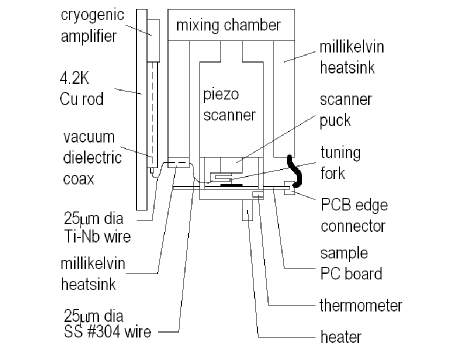
The force sensor is a quartz tuning fork (Raltron R38-32.768-12.5) with a sharpened W tip glued to one of its tines.ral The sub-pW power dissipation of the fork has no measureable effect on the base temperature of our refrigerator, and the laser-free piezoelectric detection scheme avoids problems with light sensitive samples. The scanner is a commercial cryogenic STM scan head (Omicron’s CryoSXMcry ) modified for SFM and mounted on the baseplate of an Oxford Kelvinox 100 dilution refrigerator. The microscope incorporates a cryogenic amplifier for maximum sensitivity and bandwidth. We use a phase-locked loop (Nanosurf easyPLLeas ) to excite the fork.
Piezoelectric quartz tuning forks have been used as force sensors in scanning probe microscopy for several years now. Mechanical and electrical modelsGrober et al. (2000); Karrai and Grober (1995); Rychen et al. (2000a, b) predict that forces acting on a fork change its resonant frequency and Q. Frictional forces change Q while conservative forces change the frequency. Our microscope uses the frequency shift as the force dependent signal, varying the tip height to maintain a constant shift while rastering over the sample surface.
Fig. 2 shows a block diagram of the microscope’s operation.
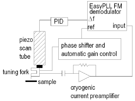
The tuning fork is excited with an AC potential applied to one of its electrodes. The other electrode is held at virtual ground by the input of a cryogenic transimpedance amplifier, discussed below. We use a bridge circuitGrober et al. (2000) to eliminate the effects of stray capacitance between the two electrodes. The current flowing between the two electrodes, as measured by the transimpedance amplifier, is a simple but effective way to measure the motion of the fork.
We use a phase-locked loop to monitor the frequency of the fork and to insure that it is always driven on resonance.Albrecht et al. (1991) This PLL has a nominal sensitivity of 5 mHz in a 1 kHz bandwidth, but we obtain a sensitivity less than this in practice, typically a few tens of mHz. This sensitivity is limited primarily by white noise from the cryogenic amplifier near the resonant frequency.
The scanner was originally designed designed for STM at 4.2 K in a helium exchange gas environment. We have detached the scan head from its original mounting rod and attached it to the base plate of the dilution refrigerator. The high-voltage signals for piezo control are carried on twisted pairs from room temperature to 4.2 K and on superconducting twisted pairs from 4.2 K to the mixing chamber, thereby minimizing Johnson heating of the refrigerator while scanning. In contrast with Omicron’s intended configuration, we scan the tuning fork with the sample fixed. This allows us to connect multiple leads to the sample and to control its temperature more easily.
The maximum 135 V scan voltage provided by the Omicron electronics gives a range of 35 m x 35 m at room temperature. This decreases to 7 m x 7 m at 4.2 K and below, a range that is frequently too small to be useful. The z-range similarly decreases from 2.7 m to 0.5 m. To increase the scan range at low temperatures we have added an additional high-voltage amplifier (RHK HVA-900rhk ) that provides scan voltages up to 450 V, yielding a maximum scan range of 22 m x 22 m and a maximum z-range of 1.8 m below 4.2 K. The scanner also provides a slip-stick based coarse motion both in the x-y plane and in the z-direction. Motions of a few mm in x and y and up to a few cm in z is possible. However, we have at times found coarse motion in the x-y plane to be unreliable.
III Cryogenic Amplifier Electronics
The microscope requires a transimpedance amplifier to measure the current through the tuning fork while scanning. The same amplifier measures the current through an SET while probing. To decrease the unavoidable parasitic capacitances in these measurements we have constructed a cryogenic amplifier and placed it near the sample on a copper rod heat sunk to 4.2 K. As an added benefit the cryogenically cooled current-sensing resistor has significantly lower Johnson noise than it has at room temperature. The amplifier is based upon a low-noise silicon JFET (Moxtek MX120,mox input-referred voltage noise 3 nV, 1/f knee below 1 kHz) that stops working below K. In order to maintain most of the circuit at 4.2 K while allowing the JFET to heat above 60 K we have designed the circuit with two printed circuit boards. The lower board contains most of the circuit elements and is held at 4.2 K. The upper board containing the JFET is mounted to the lower one with ” diameter nylon standoffs. All connections between the two boards are made with 25 m diameter stainless steel wire to minimize thermal loading. The amplifier dissipates 20 mW during operation and raises the base temperature of the refrigerator by less than 0.5 mK to about 15 mK. To achieve such a small thermal load on the mixing chamber it is crucial that the copper box enclosing the amplifier is leak-tight, light-tight, and well heat sunk to the 4.2 K bath. A charcoal sorb inside the box captures residual gas that otherwise would prevent the JFET from heating properly.
The input to the amplifier is capacitively coupled via a 4.7 nF capacitor and a coaxial cable to one of the tuning fork electrodes, and via the metallization on the tuning fork to the conducting probe tip. We capacitively couple the signal to avoid problems with DC offsets. For thermalization at the mixing chamber the coax has a 2 cm length of Stycast 2850FT as its dielectric, which contributes 18 pF stray capacitance to ground. The remainder of the coax has a vacuum dielectric to minimize its capacitance, so that the total stray input capacitance, including the gate capacitance of the JFET, is only 35 pF. This means that for a 50 k SET the bandwidth of measurement is limited to kHz. Higher speeds are possible only at the expense of further noise.
IV Scan Modes
For the purposes of locating micron-sized pads and contacting a large number of them in a reasonable period of time, scan speed rather than scan resolution is the critical factor. We would ideally like to scan the entire 22 m range of the scanner in a few minutes. We have investigated three different force regimes or scan modes: a short-range repulsive force mode, a weaker attractive force mode, and a long-range electrostatic force mode. The repulsive mode, corresponding to positive frequency shifts of a few Hz, yields the highest resolution images but is the least useful for our purposes. The very small tip-sample separation and highly nonlinear frequency vs. separation dependence make optimization of the feedback loop difficult and leads to frequent tip crashes at reasonable speeds. Faster scanning is possible with a weaker attractive force, corresponding to negative frequency shifts of a few hundred mHz. However, with this scan mode we were only successful using smaller, more sensitive forks that have other disadvantages as explained below in Section VII. The fastest scanning is obtained by charging up the tip through a diode, so that it feels a strong attractive force from the image charges in the sample.Seo et al. (2002) The resulting force is of sufficient range to have easily measured effects even with tip-sample separations greater than 50 nm. This scan mode even works on insulating substrates (e.g. SiO2) provided that the dielectric constant of the substrate differs from that of the vacuum, and yields scanning speeds of 20 m/s or more.
V Samples
Our samples consist of a 100 m x 100 m array of Al-AlO2-Al SET’s fabricated with standard e-beam lithography and double-angle evaporation.Dolan (1977) Each SET has a small island weakly coupled to source and drain leads via oxide tunnel barriers and capacitively coupled to a gate. The drain-source current is strongly dependent on gate voltage, provided that the resistance of the tunnel junctions is k.Fulton and Dolan (1987) A schematic of the sample layout is shown in Fig. 3.
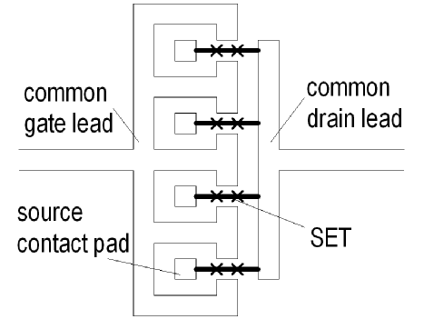
Within the array, all of the SET gate terminals are wired to a single coaxial lead, and all of the drain terminals to another. The source terminal of each SET is connected to its own 3 m x 3 m Pt contact pad.
Sample fabrication proceeds through three layers of lithography. First the common gate and drain leads as well as the source contact pads are patterned with photolithography. A trilayer consisting of 30 Å Ti, 120 Å Pt, and 2500 Å Au is deposited. Second, we mask the Au bond pads with another layer of photolithography and etch the Au away near the sample center to expose the Pt layer. This leaves a thick Au layer for the bond pads but a thin Pt layer for the SET array. The array metallization needs to be both thin and oxide free. Thin metallization allows us to increase the scan speed of the microscope. The metal surface must be oxide free to insure low resistance contact between it and the Al SET lithography, as well as to insure low resistance contact between the contact pads and the microscope tip during probing. Third, we use standard e-beam lithography to write the SET’s and ash the sample to remove any organics. The sample is attached with a spring clip to a printed circuit board, and Au wires are attached to the lithographically defined leads. It is important that the wires all come off the sample in a single direction, away from where the scanned probe will be, so as not to obstruct its motion.
Typical measurements proceed in two sequential steps. First we scan the surface of the sample until we find an SET of interest. Then we turn off the tip-sample feedback loop and establish electrical contact between the probe tip and the Pt contact pad (lightly crash the tip). An AC voltage (50 - 100 kHz) is applied to the drain lead, and the current through the SET is monitored with the cryogenic amplifier and a lock-in.
The only topographic information required for this measurement is the location of the contact pads. These are large and separated from the surrounding lithography by 2 m on all sides. Therefore the required resolution of the SFM is only about 1 m. This fact is important as the probe resolution tends to deteriorate over time with repeated probing and cleaning.
VI Results and Discussion
Fig. 4 is an image taken at millikelvin temperature showing part of an SET array.
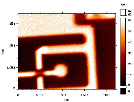
The image clearly demonstrates resolution well below 1 m at a scan speed of 15 m/s and a scan range of 22 m. Although we observe no extra heating of the refrigerator while the scan piezo is held motionless, there was enough heating during scanning to raise the temperature of the sample from 15 mK to 190 mK. The amount of heating depends strongly on the scan size and speed. In practice this heating should not cause problems because the piezo is held motionless while probing an SET.
We have electrically probed several SET’s on multiple samples. Fig. 5 shows characteristic coulomb blockade oscillations.

A 100 kHz, 100 V rms voltage was applied to the drain lead, and the in-phase component of the resulting AC current was measured by a lock-in. The SET was kept in the normal state by a 1 T magnetic field. The current never drops all the way to zero on the modulation curve because the 100 V rms drain-source voltage is larger than the coulomb blockade plateau. We observed flicker noise in these measurements far in excess of what we would expect and are conducting further experiments to determine the source.
We also made measurements of the charge sensitivity of the SET/amplifier configuration. Applying a known amount of charge to the gate of the SET and measuring the response at the output of the lock-in calibrates the gain. Comparing this gain with the noise measured at the output of the lock-in gives the charge sensitivity. For our most recent devices with resistance 80 k we have measured a charge sensitivity of . This sensitivity is limited by the Johnson noise of our feedback resistor (20 ) and by the input-referred voltage noise of our amplifier. The equivalent current noise values are 20 and 38 , comparable to the intrinsic shot noise of the SET.
VII Experimental Challenges
Following the advice of Giessibl,Giessibl (1998) we at one point tried to use smaller forks with an entire prong glued down. A smaller spring constant should yield higher force sensitivity, and gluing down an entire prong should give a Q independent of the mass of the tip, while for a fork glued only at its base the tip mass breaks the symmetry of the tines and leads to dissipation. However, we found that tuning forks with an entire prong glued down exhibit a strong coupling with the piezo scan tube. This manifests itself as seemingly random shifts in the fork resonant frequency when the scan tube expands or contracts, making scanning difficult or impossible. We observed no similar shifts using forks glued only at the base, presumably because in this case the vibration is decoupled from its support. In constrast, a fork with its entire prong glued down incorporates its support structure into the system, and we might expect that small changes in the support structure could strongly affect its vibrations. One way to avoid this problem would be to scan the sample instead of the fork.
Another challenge is to establish low-resistance contacts reliably and repeatably between the Pt contact pads and the probe tip. We have had success with both PtIr and W tips and repeatably get contact resistances less than 1 k, although to date we have been most successful using W tips. We expected to have no difficulties with PtIr tips due to the lack of native oxide but found that they were contaminated easily. Therefore we inevitably need to clean the tip with field-emission into the sample before making the first contact after cooldown. With the tip only 1 nm away from the sample surface we apply successively more negative voltages until we see an abrupt increase in the tip-sample current, indicating a clean tip. To maintain a clean sample surface while cooling we take care to maintain its temperature above that of the walls of the vacuum space, insuring that any contaminants condense on the walls instead.Rychen et al. (1999)
VIII Conclusions and Prospects
We have successfully demonstrated a scanning force microscope with sub-micron resolution at dilution refrigerator temperatures and in high magnetic fields. By imaging the sample to locate individual SET’s within a large array and making electrical contact to each SET in turn with the conducting probe tip, we can measure large numbers of SET’s with low noise and high bandwidth during a single cooldown. While our application is to arrays of SET’s, the cryogenic scanned probe could be applied to many other situations where it is necessary to measure large numbers of high-impedance nanostructures.
Acknowledgements.
We thank Thomas Ihn, Barry Barker, and Ray Phaneuf for helpful discussions. This work was supported by the Advanced Research and Development Activity and the National Security Agency.References
- Pelekhov et al. (1999) D. V. Pelekhov, J. B. Becker, and G. Nunes, Jr., Rev. Sci. Instrum. 70, 114 (1999).
- Rychen et al. (1999) J. Rychen, T. Ihn, P. Studerus, A. Herrmann, and K. Ensslin, Rev. Sci. Instrum. 70, 2765 (1999).
- Eriksson et al. (1996) M. A. Eriksson, R. G. Beck, M. Topinka, J. A. Katine, R. M. Westervelt, K. L. Campman, and A. C. Gossard, Appl. Phys. Lett. 69, 671 (1996).
- Tessmer et al. (1998) S. H. Tessmer, P. I. Glicofridis, R. C. Ashoori, L. S. Levitov, and M. R. Melloch, Nature 392, 51 (1998).
- Vančura et al. (2003) T. Vančura, S. Kičin, T. Ihn, and K. Ensslin, Appl. Phys. Lett. 83, 2602 (2003).
- Crook et al. (2003) R. Crook, A. C. Graham, C. G. Smith, I. Farrer, H. E. Beere, and D. A. Ritchie, Nature 424, 751 (2003).
- Kane et al. (2000) B. E. Kane, N. S. McAlpine, A. S. Dzurak, R. G. Clark, G. J. Milburn, H. B. Sun, and H. Wiseman, Phys. Rev. B 61, 2961 (2000).
- Schoelkopf et al. (1998) R. J. Schoelkopf, P. Wahlgren, A. A. Kozhevnikov, P. Delsing, and D. E. Prober, Science 280, 1238 (1998).
- Visscher et al. (1996) E. H. Visscher, J. Lindeman, S. M. Verbrugh, P. Hadley, J. E. Mooij, and W. van der Vleuten, Appl. Phys. Lett. 68, 2014 (1996).
- Pohlen et al. (1999) S. L. Pohlen, R. J. Fitzgerald, J. M. Hergenrother, and M. Tinkham, Appl. Phys. Lett. 74, 2884 (1999).
- Stevenson et al. (2002) T. R. Stevenson, F. A. Pellerano, C. M. Stahle, and R. J. Schoelkopf, Appl. Phys. Lett. 80, 3012 (2002).
- (12) Part No. R38-32.768-12.5, Raltron Electronics Corp., Miami, Florida.
- (13) CryoSXM, Omicron NanoTechnology GmbH, Taunusstein, Germany.
- (14) EasyPLL, Nanosurf AG, Liestal, Switzerland.
- Grober et al. (2000) R. D. Grober, J. Acimovic, J. Schuck, D. Hessman, P. J. Kindlemann, K. Karrai, I. Tiemann, and S. Manus, Rev. Sci. Instrum. 71, 2776 (2000).
- Karrai and Grober (1995) K. Karrai and R. D. Grober, Appl. Phys. Lett. 66, 1842 (1995).
- Rychen et al. (2000a) J. Rychen, T. Ihn, P. Studerus, A. Herrmann, K. Ensslin, H. J. Hug, P. J. A. van Schendel, and H. J. Güntherodt, Rev. Sci. Instrum. 71, 1695 (2000a).
- Rychen et al. (2000b) J. Rychen, T. Ihn, P. Studerus, A. Herrmann, K. Ensslin, H. J. Hug, P. J. A. van Schendel, and H. J. Güntherodt, Applied Surface Science 157, 290 (2000b).
- Albrecht et al. (1991) T. R. Albrecht, P. Grütter, D. Horne, and D. Rugar, J. Appl. Phys. 69, 668 (1991).
- (20) HVA-900, RHK Technology Inc., Troy, Michigan.
- (21) Part No. MX120, Moxtek Inc., Orem, Utah.
- Seo et al. (2002) Y. Seo, W. Jhe, and C. S. Hwang, Appl. Phys. Lett. 80, 4324 (2002).
- Dolan (1977) G. J. Dolan, Appl. Phys. Lett. 31, 337 (1977).
- Fulton and Dolan (1987) T. A. Fulton and G. J. Dolan, Phys. Rev. Lett. 59, 109 (1987).
- Giessibl (1998) F. J. Giessibl, Appl. Phys. Lett. 73, 3956 (1998).