Observation of disorder-induced weakening of electron-phonon interaction in thin noble metal films
Abstract
We have used symmetric normal metal-insulator-superconductor (NIS) tunnel junction pairs, known as SINIS structures, for ultrasensitive thermometry in the temperature range 50 - 700 mK. By Joule heating the electron gas and measuring the electron temperature, we show that the electron-phonon (e-p) scattering rate in the simplest noble metal disordered thin films (Cu,Au) follows a temperature dependence, leading to a stronger decoupling of the electron gas from the lattice at the lowest temperatures. This power law is indicative e-p coupling mediated by vibrating disorder, in contrast to the previously observed and laws.
pacs:
PACS numbers: 72.10.Di, 72.15.Eb, 74.50.+r, 63.20.KrAlthough the interaction between conduction electrons and thermal phonons is elementary for many processes and phenomena at low temperatures, there are still relatively few experimental studies that conclusively support the theoretical description, particularly for typical disordered thin film samples. Several earlier results rou ; kansk ; urbina indicated that even for disordered films, the temperature dependence for the electron-phonon (e-p) scattering rate follows the power law expected for pure samples with coupling to longitudinal phonons only gant : . These results confirmed the relation between heating power and electron and phonon temperatures and in a volume , and it is widely used for thin film metallic samples at low temperatures ( is a material dependent parameter). However, the theory for disordered thin films schmid ; alt ; reiz ; serg predicts that the scattering rate from vibrating disorder (impurities, boundaries etc.) is in the limit , where is the wavevector of the dominant thermal phonons and the electron mean free path. This leads to the relation
| (1) |
a result that has not been widely confirmed. In fact, we are not aware of any observation of it in standard normal metal films like Cu, Al, Au etc., and some evidence exists only for strongly disordered ( nm) Ti, Hf ger and Bi kom films.
Here, we report the observation of disorder-weakened electron-phonon (e-p) scattering in ordinary evaporated Cu and Au thin films. We have measured the rate at which electrons in a normal metal wire overheat, when DC power is applied to it by Joule heating, at sub-Kelvin temperatures jenni . This technique has been shown rou ; kansk ; urbina to give the energy-loss rate directly, in contrast to the temperature dependence of the weak localization resistance lin , which gives the dephasing rate depha . The overheating rate is determined by measuring the electron temperature directly with the help of symmetric normal metal-insulator-superconductor (NIS) tunnel junction pairs, known as SINIS structures. SINIS-thermometers have been shown row ; nah1 ; leivo to be extremely sensitive thermometers, operating at the lowest experimentally achievable temperatures. Therefore, they are also candidates for ultrasensitive microbolometers Nahum ; Kuzmin in the sub-Kelvin temperature range.
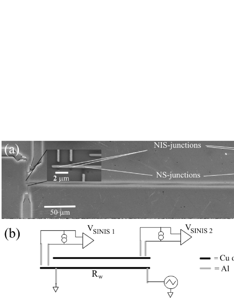
All the samples used in this work have two normal metal wires of length 500 m, and width 300-400 nm, separated by a distance 2 m and electrically isolated from each other, as shown in the SEM image [Fig. 1(a)]. They were fabricated by e-beam lithography and three-angle shadow-mask evaporation technique on thermally oxidized (oxide thickness 250 nm) Si substrates, with film thicknesses varying from 33 nm to 140 nm, corresponding to a measured 24-53 nm. The deposition was done by e-beam evaporation in a UHV chamber with a growth rate Å/s.
The normal metal wires were connected to the measurement circuit by superconducting Al leads. One pair of leads forms SINIS tunnel junctions for each wire, and are used to measure the electron temperature of the normal metal wire. These tunnel junctions were formed by thermal oxidation of the Al films, yielding tunneling resistances 20-50 k, typically. In contrast, the junctions connecting the lower wire in Fig. 1 to a voltage source are NS-junctions without tunneling barriers, and are used to heat the sample. Clean NS-junctions have a small electrical resistance compared to the residual low-temperature resistance of the wire, between 100 and 1500 for all the samples. For all heating voltages used in this paper, we have measured that the NS-junctions are biased within the superconducting gap of the leads. Then, the process of Andreev reflection can take place, making the junctions good thermal insulators despite being electrically conducting. This way we can achieve conditions in which the wire is uniformly Joule heated short . Moreover, since the wires are much longer than a typical electron-electron scattering length hug , the electrons in the wire have a well defined Fermi-distribution, and a temperature . In addition, the effect of multiple Andreev reflections on the distribution is negligible for these wire lengths anne . Also, the thermal resistance of the tunnel junctions is estimated to be at least an order of magnitude larger than the thermal resistance due to the e-p coupling at the temperature range of this experimentdragos , and can be neglected in the analysis.
All measurements were performed by current biasing the two SINIS thermometers and measuring their DC voltages simultaneously [Fig 1(b)] in a dilution refrigerator with a base temperature mK. All wiring connected to the sample was filtered at 4.2 K, to minimize the overheating by external noise. This was seen to be very critical for good measurements at the lowest temperatures, as we also performed measurements without the filtering, and observed significant overheating below 0.3 K. The SINIS thermometers were calibrated by varying the bath temperature () of the refrigerator very slowly, to ensure the sample stage was in equilibrium with the bath. The temperature of the sample stage was measured with a calibrated Ruthenium Oxide thermometer.
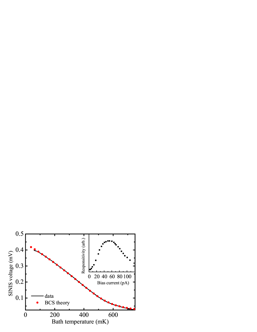
Figure 2 shows an example of a calibration measurement. The theoretical points (red) were calculated numerically from the BCS theory. This calculation has essentially no free parameters, since the current bias is known, and and are determined independently from the I-V characteristics (not shown). The agreement with the data is good except at the very lowest temperatures, where a slight deviation can be seen below 0.1 K. This deviation could arise by at least two major mechanisms: (i) a component of leakage or noise current affects the measurement, and (ii) the electrons overheat at the low- range (). We have ruled out (i) by directly measuring the responsivities of the thermometers as a function of using a lock-in amplifier (Fig. 2 inset). The theoretical is a monotonically decreasing function of . However, experimentally at low the responsivity deviates from theory, and we find a maximum. Thus, by setting the bias current above the maximum ( pA in Fig. 2 inset), where the BCS-theory is accurate, problem (i) can be avoided. Mechanism (ii), overheating by noise power is an obvious explanation, since we observed a clear improvement with added filtering of the lines. Thus, at the lowest temperatures ( K) the SINIS thermometers start to saturate to a temperature determined by the absorbed noise power , where depending on the mechanism of e-p scattering involved. The correct is therefore always given by the BCS-theory function, instead of the measured phenomenological plot.
Using the calibrated SINIS thermometers, we then studied what happened when only the lower wire is directly heated by Ohmic dissipation at 60 mK. Heating power was applied by slowly ramping a DC voltage across the wire, and determined by measuring the heating current and voltage directly in a 4-wire configuration. In all the samples studied, the temperature of the upper wire rises also, when the lower wire is heated jenni . This indirect heating can be either due to phonons emitted from the hot wire and backscattered, or by photons (thermal noise) coupling capacitively. Since we don’t know the relative contributions of these two channels, we only obtain an upper limit for the local phonon temperature fooot . However, the main conclusion is that all the data satisfy the condition for powers , and the error introduced by approximating Eq. (1) by is less than 4% (for 6%). Thus, analysis can proceed without the knowledge of , and the slope of vs. in a log-log plot will directly give . We also note that thermal relaxation by radiation into the leads sch is estimated to be insignificant compared to the e-p scattering, due to the large volume of our samples.
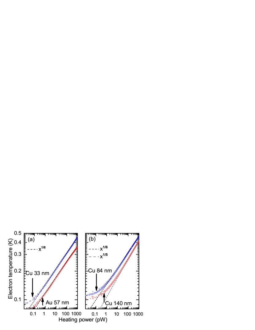
In Fig. 3 we plot the electron temperatures in the heated wire vs. obtained from several sweeps for four different samples in log-log scale. Data for the thinner Cu and Au samples is shown in Fig. 3(a), whereas Fig. 3(b) plots the results for the thicker Cu samples. The agreement with is strikingly good for the thin Cu and Au samples, from pW to nW. The 84 nm thick Cu sample also agrees with at higher power, but the thickest Cu sample does not, and is consistent with . The saturation of by at the lowest is clearly visible for all the samples, and the effect seems to be stronger for the thicker Cu samples. This is most likely due to the changing resistance of the wire: the thicker wires have lower resistance approaching the characteristic impedance of the wiring, causing more absorption of .
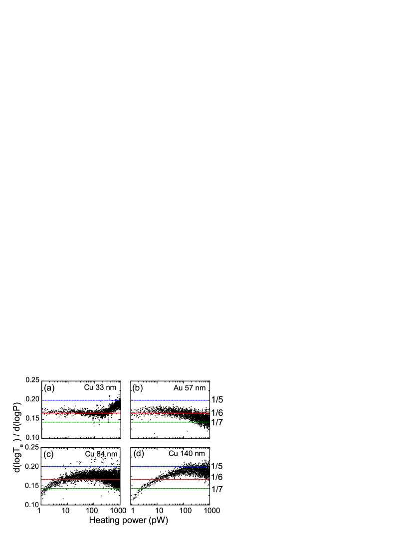
To obtain a more detailed picture, we also plot the numerically computed logarithmic derivatives of the data vs. in Fig. 4. Even though numerical differentiation is sensitive to noise, we can still strengthen our case. Again, for the thinner samples is obviously more consistent than any other integer power. Some deviations start to appear above a few hundred pW, which are not fully understood at the moment. The thicker samples show the effect of by a smooth increase of the derivative at low powers. However, the 84 nm thick sample does seem to develop a plateau at around , whereas the thickest sample is more consistent with in the high power limit.
By determining the volumes of the normal metal wires accurately with AFM and SEM measurements, we can extract the parameters and from the one parameter fits in Fig. 3. We get for the Cu samples W/K6m3 ( nm), W/K6m3 ( nm) and W/K5m3 ( nm), whereas for the Au sample W/K6m3. We note that the value of in the thickest Cu sample is consistent with earlier studies Nahum , since it is a material parameter in the pure limit. However, theory serg predicts that depends on the level of disorder, and thus if , each sample can have a different . This is clearly the case in our experiment. Comparing the measured with the microscopic theory, we can estimate the transverse sound velocity . We get m/s and m/s for the Cu wires nm and nm, respectively, and m/s for the Au wire, a reasonable result. As the bulk longitudinal sound velocities in Cu and Au are about twice as large, we have indirect evidence that transverse modes are dominant for .
In conclusion, we have for the first time obtained clear evidence that the electron-phonon scattering rate scales with temperature as in disordered, evaporated Cu and Au thin films. This power law corresponds to electrons scattering from phonons mediated by vibrating disorder. In our measurement boundary scattering is likely to be significant, since . In contrast, e-p scattering in the presence of static disorder leads to , a result that has been confirmed in many materials and samples lin . Our result has several practical consequences. Compared to a lower power dependence, it is harder to cool the electrons with cold phonons, i.e. the electron gas decouples from the lattice more strongly at the lowest temperatures. Direct electron cooling nah1 ; leivo then becomes more important. On the other hand, a sensor based on the hot electron effect is even more sensitive, since the ultimate noise equivalent power of such a detector is proportional to . We stress that in order to obtain the sample needs to be a regular metal, have , contain little non-vibrating disorder and have 3D phonons coupled to electrons by the deformation potential. We believe most earlier experiments do not satisfy all these conditions (e.g. Ref. rou has , Ref. yung has a suspended GaAs substrate, Refs. kansk ; urbina ; ditusa studied alloys and Ref. kivin studied degenerately doped Si in the strong screening limit.)
We thank D.-V. Anghel, A. N. Cleland, J. P. Pekola, H. Pothier, A. Savin and A. Sergeev for discussions. This work was supported by the Academy of Finland under the Finnish Center of Excellence Program 2000-2005 project No. 44875, and by the projects No. 105258 and 205476 (TULE programme).
References
- (1) M. L. Roukes, M. R. Freeman, R. S. Germain, R. C. Richardson, and M. B. Ketchen, Phys. Rev. Lett. 55, 422 (1985).
- (2) M. Kanskar and M. N. Wybourne, Phys. Rev. Lett. 73, 2123 (1994).
- (3) F. C. Wellstood, C. Urbina, and J. Clarke, Phys. Rev. B 49, 5942 (1994).
- (4) V. F. Gantmakher, Rep. Prog. Phys. 37, 317 (1974).
- (5) A. Schmid, Z. Phys. 259, 421 (1973); in Localization, Interaction and Transport Phenomena, Springer 1985.
- (6) B. L. Altshuler, Zh. Eksp. Teor. Fiz. 75, 1330 (1978) [Sov. Phys. JETP 48, 670 (1986)].
- (7) M. Yu. Reizer and A. V. Sergeev, Zh. Eksp. Teor. Fiz. 90, 1056 (1986) [Sov. Phys. JETP 63, 616 (1986)].
- (8) A. Sergeev and V. Mitin, Phys. Rev. B 61, 6041 (2000); Europhys. Lett. 51, 641 (2000).
- (9) M. E. Gershenson, D. Dong, T. Sato, B. S. Karasik, and A. V. Sergeev, Appl. Phys. Lett. 79, 2049 (2001).
- (10) Yu. F. Komnik, V. Yu. Kashirin, B. I. Belevtsev, and E. Yu. Beliaev, Phys. Rev. B 50, 15 298 (1994).
- (11) J. T. Karvonen, L. J. Taskinen, and I. J. Maasilta, Phys. Stat. Sol. (c) 1, 2799 (2004).
- (12) For a recent review of the weak localization data, see J. J. Lin and J. P Bird, J. Phys. Condens. Matter 14, R501 (2002).
- (13) The dephasing rate can equal the energy loss rate if the electron-phonon interaction is the only dephasing mechanism present. In general, one can imagine many other dephasing channels that do not influence the energy loss rate, a prime example being the electron-electron interaction, which by definition cannot lower the energy of the electron gas as a whole.
- (14) J. M. Rowell and D. C. Tsui, Phys. Rev. B 14, 2456 (1976).
- (15) M. Nahum, T. M. Eiles, and J. M. Martinis, Appl. Phys. Lett. 65, 3123 (1994).
- (16) M. M. Leivo, J. P. Pekola, and D. V. Averin, Appl. Phys. Lett. 68, 1996 (1996).
- (17) M. Nahum and J. Martinis, Appl. Phys. Lett. 63, 3075 (1993).
- (18) D.-V. Anghel and L. Kuzmin, Appl. Phys. Lett. 82, 293 (2003); L. Kuzmin, D. Chouvaev, M. Tarasov, P. Sundquist, M. Willander and T. Claeson, IEEE Trans. Appl. Supercond. 9, 3186 (1999).
- (19) For much shorter but otherwise equivalent wires, the NS junctions are quickly biased above the gap, and the heat leak through them has to be taken into account in the analysis kivi .
- (20) J. M. Kivioja, I. J. Maasilta, J. P. Pekola, and J. T. Karvonen, Physica E 18, 21 (2003).
- (21) H. Pothier, S. Guéron, Norman O. Birge, D. Esteve, and M. H. Devoret, Phys. Rev. Lett. 79, 3490 (1997).
- (22) F. Pierre, A. Anthore, H. Pothier, C. Urbina, and D. Esteve, Phys. Rev. Lett. 86, 1078 (2001); H. Pothier, private communication.
- (23) D. V. Anghel and J. P. Pekola, J. Low Temp. Phys. 123, 197 (2001).
- (24) Since the two wires are separated by only m, a distance much shorter than the lateral mean free path of phonons in SiO swar , it is reasonable to assume that the phonon temperatures are equal in the two wires.
- (25) E. T. Swartz and R. O. Pohl, Rev. Mod. Phys. 61, 605 (1989).
- (26) D. R. Schmidt, R. J. Schoelkopf, and A. N. Cleland, Phys. Rev. Lett. 93, 045901 (2004).
- (27) P. Kivinen, A. Savin, M. Zgirski, P. Törmä, J. Pekola, M. Prunnila, and J. Ahopelto, J. Appl. Phys. 94, 3201 (2003).
- (28) C. S. Yung, D. R. Schmidt, and A. N. Cleland, Appl. Phys. Lett. 81, 31 (2002).
- (29) J. F. DiTusa, K. Lin, M. Park, M. S. Isaacson, and J. M. Parpia, Phys. Rev. Lett. 68, 1156 (1992).