Photon-assisted transport in semiconductor nanostructures
Abstract
In this review we focus on electronic transport through semiconductor nanostructures which are driven by ac fields. Along the review we describe the available experimental information on different nanostructures, like resonant tunneling diodes, superlattices or quantum dots, together with the theoretical tools needed to describe the observed features. These theoretical tools such as, for instance, the Floquet formalism, the non-equilibrium Green’s function technique or the density matrix technique, are suitable for tackling with photon-assisted transport problems where the interplay of different aspects like nonequilibrium, nonlinearity, quantum confinement or electron-electron interactions gives rise to many intriguing new phenomena. Along the review we give many examples which demonstrate the possibility of using appropriate ac fields to control/manipulate coherent quantum states in semiconductor nanostructures.
keywords:
Photon assisted tunneling, nanostructuresPACS:
73.40.Gk, 73.50.Fq, 73.63.Hs, 73.63.Kv1 Introduction
Interaction with external time-dependent fields in low-dimensional systems leads in many cases to completely new ways of electronic transport. In this review we shall focus on electronic transport through semiconductor nanostructures like resonant tunneling diodes, superlattices or quantum dots where the peculiar synergism between ac fields and quantum confinement gives rise to many novel phenomena. Among them we can mention ac-induced absolute negative conductance and the so-called dynamical localization phenomenon observed in superlattices, electron pumps realized in different nanostructures or the very recent microwaves studies demonstrating quantum coherence in double quantum dots.
Historically, the first experiments of ac-driven tunneling date back to the early sixties when Dayem and Martin [1] studied photon-assisted-tunneling (PAT) in superconductor-insulator-superconductor hybrid structures. Soon afterwards, Tien and Gordon proposed a simple model of PAT (Section 2) in terms of ac-induced side-bands [2]. During the last few decades, this Tien-Gordon model, based on the Bardeen Hamiltonian, has been shown to grasp the main qualitative physics for PAT through different nanostructures and mesoscopic devices. In the first part of this review we shall discuss different theoretical techniques which allow to address PAT in semiconductor nanostructures where a treatment beyond the simple Tien-Gordon model is called for. In this part we shall describe the Floquet approach (Section 3), various methods based on the Scattering formalism (Section 4), and two methods based on nonequilibrium Green’s functions (Section 5).
After these four sections devoted to theoretical techniques for the study of PAT, we elucidate the physics of PAT, both from the experimental and theoretical points of view, in different semiconductor nanostructures. Here, we chose to divide this part of the review according to the nanostructure described. This division of the review begins with Section 6 where we describe PAT in resonant tunneling diodes. After a short description of the experiments of Chitta et al [3] where the far infrared response of double barrier structures was analyzed, we elaborate on the importance of studying PAT in these systems with models including mixing of electronic states due to the external field: when the resonant states in the quantum well are strongly coupled to reservoirs a description in terms of extended states is called for. We discuss how mixing of electronic states can be incorporated into the Transfer Matrix (subsection 6.1) and the Transfer Hamiltonian (subsection 6.5) methods. This Section is completed with discussions about the effects of external magnetic fields (subsection 6.3) and charge accumulation effects (subsections 6.6 and 6.7) on PAT.
The influence of time-dependent fields on transport through semiconductor superlattices is discussed in Section 7. We start this Section by discussing the intringuing phenomenon of absolute negative conductance observed in THz irradiated superlattices [4] in the linear transport regime (subsection 7.1). Next, we discuss the nonlinear transport regime. In this regime, semiconductor superlattices exhibit strongly nonlinear behavior due to the combined action of tunneling and Coulomb interactions. In particular, weakly coupled superlattices have been shown to exhibit electric-field domain formation, self-sustained oscillations and driven and undriven chaos. Perturbing the system with an ac field brings about a great deal of new transport phenomena. We divide this part into four subsections where the statics and dynamics of undriven (subsections 7.2 and 7.3) and ac-driven (subsections 7.4 and 7.5) superlattices are elucidated. Finally, this portion of the review ends with a subsection devoted to strongly coupled superlattices (subsection 7.6).
During the last few years, many of the new developments in the field of PAT have been realized in quantum dots111A review on this subject, with a more limited scope, has been recently published in Ref. [5].. We elaborate on different aspects of these new developments in Sections 10-12. Beginning with Section 10 we discuss PAT in the Coulomb blockade regime. In this Section, key concepts like PAT spectroscopy through zero-dimensional states are introduced. Section 11 is devoted to double quantum dots where exciting new experiments studying the influence of microwaves on the transport properties of these devices have spurred a great deal of theoretical activity. Of special interest here is the regime where the effective Hilbert space of the double quantum dot can be reduced to just a few levels. Understanding the interplay between electron correlations and the driving field in these cases is of outmost importance, both from the fundamental and applied points of view. In particular, the ability to rapidly control electrons using ac fields has immediate applications to quantum metrology and quantum information processing. Finally, the last Section of this part devoted to quantum dots focuses on strongly correlated quantum dots (Section 12). Here, we analyse the influence which an external ac field has on quantum dots in the Kondo regime (subsection 12.1), in one-dimensional quantum dots (subsection 12.2) and in quantum dots in the Wigner molecule regime (subsection 12.3).
The review is completed with three thematic Sections. The first one (Section 8) gives a short account of recent experiments showing microwave-induced zero resistance in two-dimensional electron gases at low magnetic fields and their explanation in terms of photon-assisted excitations to higher Landau levels. In the second Section we give a brief introduction to electron pumps (Section 9), a rapidly evolving area of research which, surely, would deserve a review of its own. For completeness, we also include a short description about photon-assisted shot noise (Section 13) another fascinating area of research which has rapidly developed during the last few years222Here we urge the interested reader to consult the excelent review on shot noise by Blanter and Buttiker in Ref. [6]..
2 Tien-Gordon model
Motivated by the experimental microwave studies in superconductor-insulator-superconductor tunnel junctions of Dayem and Martin [1], Tien and Gordon [2] presented a theoretical model which, in spite of its simplicity, has proven to be very successful in describing qualitatively transport in ac-driven nanostructures. The reason for this success is that Tien and Gordon’s simple model already contains the main physical ingredient of photon assisted tunneling: the idea that a time dependent potential can induce inelastic tunnel events when the electrons exchange energy quanta, i.e. photons, with the oscillating field.
The first configuration discussed by Tien and Gordon consists of an electric field applied normal to the surfaces of the superconducting films. The electric field sets up a potential difference between the films. Neglecting the interaction of the microwave field with the insulating barrier and considering one of the metallic films as a reference (left region), the effect of the microwave field is to add a potential to the other metallic film (right region). Importantly, within this simple model the effect of the external field is accounted for by adding a time-dependent, but spatially constant, potential in the right region which is described by a local Hamiltonian:
| (1) |
It is obvious that the time-dependent potential does not vary the spatial distribution of the electronic wave function within each region. Solving the time-dependent Schrödinger equation, the electronic wave function for the right region can be written as:
| (2) | |||||
where the relationship:
| (3) |
with being the Bessel function of -th order, has been used. From the previous expression of the wave function, it can be observed that tunneling between the superconducting films through the insulating barrier can happen from states of energy in the left region to states of energy in the right region, namely through inelastic tunneling. The time-averaged spectral density, , for the right region can be written in terms of the density of states without external potential, , as:
| (4) |
Eq. (4) can be interpreted physically as follows: photon absorption () and emission () can be viewed as creating an effective electron density of states at energies with a probability given by .
The tunneling current between the superconducting films can be obtained by means of the Transfer Hamiltonian (TH) method 333The Transfer Hamiltonian method, also called Bardeen Hamiltonian method, considers the coupling between the different parts of the system only to lowest order in perturbation theory [7].. Assuming that the transmission coefficient does not depend on energy, the tunneling current can be expressed as [7, 8, 9]:
| (5) |
where is the transmission coefficient, which is assumed constant, is the Fermi-Dirac distribution function and the applied dc voltage.
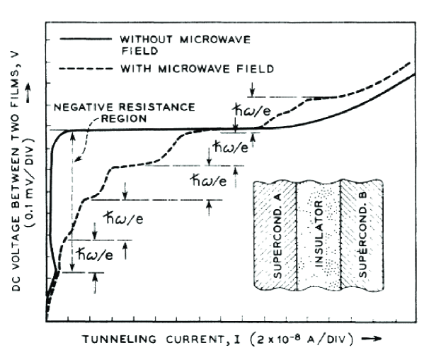
In the presence of microwaves and considering the explicit expressions for the spectral densities (4), the dc current becomes:
| (6) | |||||
Importantly, the dc currents with and without microwaves can be related as:
| (7) |
where is the current without radiation. Namely, the rectified current of a system biased with a voltage is given as a sum of dc-currents without ac driving evaluated at voltages shifted by integer multiples of photon energies.
3 Floquet theory
In quantum mechanics, symmetry is expressed by an operator S which leaves the Schrödinger equation invariant, i.e., it commutes with the operator . Thus, the solutions of the Schrödinger equation are, besides a time-dependent phase factor, also eigenfunctions of the symmetry operator. For a Hamiltonian with -periodic time dependence,
| (8) |
the related symmetry operation is a discrete time translation by one period of the driving, . As symmetry operations have to conserve the norm of any wavefunction, the eigenvalues of are pure phase factors and one may assume for an eigenfunction the eigenvalue exp(-i): = By inserting the wavefunction () in the Schrödinger equation, one obtains . Thus for a system which obeys discrete time-translational symmetry, there exists a complete set of solutions of the Schrödinger equation which have Floquet structure,i.e., they are of the form: where .
We consider a general quantum system driven by a periodic electric field, described by a time-dependent Hamiltonian which we can divide in the following way:
| (9) |
Here holds the tunneling terms, holds the electron-electron interaction terms and describes the interaction of the system with the -periodic driving field. The periodicity of the driving field allows us to use the Floquet theorem to write solutions of the Schrödinger equation as where is called the quasi-energy, and is a function with the same period as the driving field, called the Floquet state. This type of expression is familiar in the context of solid-state physics, where spatial periodicity permits an analogous rewriting of the spatial wavefunction in terms of quasi-momenta and Bloch states (Bloch’s theorem).
The Floquet states provide a complete basis, and thus the time-evolution of a general state may be written as a superposition of Floquet states:
| (10) |
which is formally analogous to the standard expansion in the eigenvectors of a time-independent Hamiltonian. Indeed, in the adiabatic limit, , the quasi-energies evolve to the eigenenergies, and the Floquet states to the eigenstates. It is important to note that in this expansion both the basis vectors (the Floquet states) and the expansion coefficients explicitly depend on time. The nature of this time-dependence is very different however, and the superposition of the -periodicity of the Floquet states with the phase factors arising from the quasi-energies produces a highly complicated, quasi-periodic time-dependence in general.
As the Floquet states have the same period as the driving field, they are only able to produce structure in the time-dependence on short time-scales. Consequently, the dynamics of the system on time-scales much larger than is essentially determined by just the quasi-energies, and hence evaluating the quasi-energies provides a simple and direct way of investigating this behavior. A number of different methods can be used to numerically calculate the quasi-energies of a quantum system, and a detailed description of them is given in Ref. [10].
One commonly used method is
to evaluate the unitary time-evolution operator
for one period of the driving field , and then to
diagonalize it. It may be easily shown that the eigenvectors of
this operator are equal to the Floquet states, and its eigenvalues
are related to the
quasi-energies via .
When two quasi-energies approach degeneracy the time-scale for
tunneling between the states diverges, producing the phenomenon of
coherent destruction of tunneling (CDT) [11]. The
time scale for localization is the inverse of the energy
separation of the quasienergies.
For instance, in a two level system
driven by a term ,
CDT can be understood from the
renormalization of the level splitting:
| (11) |
where is the interlevel coupling. At the first zero of , namely when , the effective tunnel splitting vanishes leading to a complete localization of the particle in the initial state. This phenomenon is also known as Dynamical Localization in the PAT literature 444Note that a more general phenomenon is also called Dynamical Localization in chaotic dynamical systems: In this context, Dynamical Localization is the phenomenon by which destructive interference effects supress difussion in the relevant phase space. See Ref. [12].. The expression for the renormalization of the hopping in Eq. (11) is obtained from first-order perturbation theory in the tunneling, see subsection 3.2.
As we shall see for some specific quantum systems considered in this review, it is frequently the case that the total Hamiltonian is invariant under the generalized parity operation: . As a result the Floquet states can also be classified into parity classes, depending whether they are odd or even under this parity operation. Quasi-energies belonging to different parity classes may cross as an external parameter (such as the field strength) is varied, but if they belong to the same class the von Neumann-Wigner [13] theorem forbids this, and the closest approaches possible are avoided crossings. Identifying the presence of crossings and avoided crossings in the quasi-energy spectrum thus provides a necessary (though not sufficient) condition for CDT to occur.
An interesting effect shown by Stockburger [14] is that the condition of degenerate Floquet levels, required for localization in a symmetric system, can be substantially relaxed for tunneling systems with broken symmetry. He found that the localization regime was substantially extended due to a synergistic effect of dynamic and static asymmetry. He called this phenomena ”Non-degenerate Coherent Destruction of Tunneling” (NCDT). His results will decrease the difficulty to measure coherent destruction of tunneling, i.e, to control accurately the driving amplitude.
3.1 Perturbation theory for Floquet states
Although the quasi-energies are extremely useful for interpretation of the time-dependence of a quantum system, they are usually difficult to calculate and numerical methods must be employed. When the driving field dominates the dynamics, however, it is possible to use a form of perturbation theory introduced by Holthaus [15], in which the time-dependent part of the problem is solved exactly, and the tunneling part of the Hamiltonian, , acts as the perturbation. Using this method, Holthaus [15] and Hanggi [10, 16] have studied the two level system. For high fields, perturbation theory for Floquet states allows for an analytic description of the quasienergies and the field parameters where dynamical localization takes place.
This was generalized to treat interacting systems in Refs. [17, 18, 19] and was found to be very successful in the high-frequency regime, where is the dominant energy-scale. We now give a brief outline of this method. Inserting 10 in the Schrödinger equation, the Floquet states and their quasi-energies may be conveniently obtained from the eigenvalue equation:
| (12) |
where the hermitian Floquet operator operates in an extended Hilbert space of -periodic functions [20]. The procedure consists of dividing the Hamiltonian as in Eq. (9), and finding the eigensystem of the operator , while regarding the tunneling Hamiltonian as acting as a perturbation. Standard Rayleigh-Schrödinger perturbation theory can now be used to evaluate the order-by-order corrections to this result, requiring only that we define an appropriate inner product for the extended Hilbert space:
| (13) |
Here denotes the usual scalar product for the spatial component of the wavevectors, and is the integration over the compact time coordinate. We shall show in later sections how this method can be used to obtain analytical forms which accurately describe the behavior of the quasi-energies for the systems we study.
3.2 ac-driven two-level Systems
Holthaus [15] derived explicitly the quasienergies for a two-level system in the limit of strong electric field-electron coupling when the interlevel coupling, , can be treated perturbatively. The starting point of the derivation is the Schrödinger equation for the two level system:
| (14) |
with , and
| (15) |
is the intensity of the ac field and is the dipole matrix element between the lowest two double well eigenstates. In the strong coupling limit , the time independent part of the Hamiltonian can be treated as a perturbation and Eq. (14) reduces to:
| (16) |
A fundamental system of solutions of Eq. (16) is:
| (17) |
and are time-periodic states (Floquet states) and the quasienergies are degenerate and equal to zero (modulo ). The interlevel part of the Hamiltonian, , is now treated as a perturbation exploiting the fact that the Floquet states are stationary states in the extended Hilbert space of time-periodic functions, see Eq. (13), such that the quasienergies, (with and ) are:
| (18) |
Now, if the absolute value of the dipole matrix element is approximated by that of the positions of the center of the wells , one gets
| (19) |
This result shows that, in the presence of an ac field of intensity , the tunnel coupling is renormalized by the zero-order Bessel function, as stated in Eq. (11).
Although sinusoidal driving is considered more frequently when discussing CDT (simply because it is the natural form of electromagnetic radiation), some work has been also devoted to analyze the degree of localization induced by ac potentials with different shape. Bavli and Metiu showed that a semi infinite laser pulse is able to localize an electron in one of the wells in a double quantum well structure [21]. Holthaus investigated the effect of pulse shaping to enhance the rate of tunneling [22]. Square-wave driving has been considered to a lesser extent. It was shown in Refs. [23, 24] that total CDT can only be produced in a superlattice if the crossings of the quasienergies are equally spaced. They showed that this only occurs if the field has discontinuities, and the square-wave is the simplest example of this type. A comparision of the degree of localization in two-level systems for square-wave, sinusoidal and triangular driving was theoretically performed by Creffield [25]. He analyzed the high frequency regime, where perturbation theory in the interlevel coupling works well and the low frequency regime where the crossings move away from the values predicted by perturbation theory. The position of the crossings can fitted by the function [25]:
| (20) |
where is the n-root of , is the splitting between the two levels and the frequency of the driving field. Creffield found that the positions of the crossings at low frequencies follow (20) exactly for square-wave driving and with small deviations for other shapes of the driving field. Such a general behavior allows the positions of the quasienergy crossings to be accurately located in all regimes of driving. In spite of the reduction of the degree of localization observed at low frequencies, the accurate control of the crossings positions opens new posibilities for experimental configurations.
When the hopping increases, higher order terms should be included and CDT does not occur at the zeros of the zero-order Bessel function. Barata et al [26] have shown that the second order contribution to the renormalized hopping is identically zero and the third order contribution is different from zero just at the zeros of and is given by:
| (21) |
Recently, the perturbation series of a two-level system driven a a sinusoidal field (in the strong coupling regime) has been analyzed in detail by Frasca in Ref. [27].
The combined effect of radiation and magnetic fields in two level systems was analyzed by Villas-Boas et al. [28]. They did an analysis of the quasienergy spectrum for the case where the magnetic field is oriented perpendicular to the quantum wells interfaces and also in the case where a finite component parallel to the interfaces is applied. The analysis was performed based in the parity properties for both configurations and for all ranges of frequency and intensity of the radiation. They found that at low frequencies the Dynamical Localization points shift to lower ratios yielding to poorer localization by the ac field.
The two-level system has been exhaustively studied in the literature. However, in many mesoscopic systems the configuration is such that more than two levels interact and the analysis is more complicated. The next simplest case corresponds to a three level system. As we will describe in Section 11.6, a double quantum dot with two interacting electrons and driven by an ac field can be described by an effective six dimensional Hubbard Hamiltonian. If spin-flip processes which can arise by electron scattering with nuclei or spin-orbit interaction are not included, the spin singlet and triplet are decoupled and the effective Hamiltonian describing each sector is three dimensional. We shall describe in Section 11.6 how to obtain the Floquet spectrum by using the procedure described above, i.e, considering the interdot coupling as a perturbation in the limit of strong electric field-electron coupling.
3.3 Floquet theory for spatially periodic systems
A superlattice consists on N identical quantum wells coupled by finite barriers. For strong inter-well coupling the discrete states of each isolated quantum well hybridize with those of the neighbor wells and finite width minibands are formed.
Holthaus studied the spectrum of a superlattice under ac radiation [15, 29, 30]. In these systems, periodicity in time leads to a formulation in terms of quasienergy eigenvalues and spatial periodicity implies that the quasienergies for the allowed quantum states group together in minibands.
The Hamiltonian describing this system is:
| (22) |
where is the electrostatic potential of the superlattice. As is periodic in time, there is a complete set of Floquet wave functions as solutions of the Schrödinger equation. For large number of quantum wells N, the energies of the lowest unperturbed miniband of width are given by:
| (23) |
where is the center of the unperturbed miniband. It can be shown from a quantum mechanical calculation which neglects finite size effects (i.e., for large N) that the expression for the quasienergies originated from them is:
| (24) |
This result implies that the width of the quasienergy miniband becomes zero at zeros of [29].
A similar result is found for the average electron velocity using semiclassical arguments [31, 32]: Considering the dispersion relation for the undriven superlattice and a time dependent electric field: , the group velocity of a wave packet centered around and is given by:
| (25) |
and the velocity average over one period of the electromagnetic field is:
| (26) |
Hence if the ratio of the Bloch frequency and the external frequency is equal to a zero of , namely , the average electron velocity is zero and the wave packet becomes localized. This localization induced by ac field (Dynamical Localization) is dubbed miniband collapse by radiation in the context of superlattices.
We conclude this part by mentioning that the Floquet theory described in this section applies to closed systems. We will describe along the review how one can combine the Floquet theory with other powerful techniques, like the nonequilibrium Green’s functions technique or the density matrix technique, in order to treat open systems.
4 Scattering approach
4.1 Transfer matrix approach
Here we briefly review the transfer matrix approach proposed by Coon and Liu [34, 35, 36] to solve a general potential profile in the presence of both dc and ac signals. The approach is based on the following asumption: given an arbitrary potential profile, one can always approximate to an arbitrary accuracy the actual profile by a series of steps, namely by dividing the space into regions of constant potentials. Within this approach, one can solve the time-dependent Schrödinger equation for constant and in terms of plane waves:
| (27) |
One can easily verify that
| (28) |
is a solution with . Then, a general solution can be built up with energy components ():
| (29) |
where . If the solution in the next constant potential is :
| (30) |
a general transfer matrix M is required so that: where and similarly for b, c and d, where the superscript T means transposing the row matrix 555In order to get the matrix M one needs also to include boundary conditions. The simplest ones are to impose the continuity of the wave function and its derivative [36].. By using a similar reasoning for all potential steps, one gets the complete transfer matrix which relates the constants and on one side of the structure to and on the other side. Transmission and reflection amplitudes fon an incident electron with energy are found by setting , , and . Then, a multichannel scattering state consists of the incident wave and the scattered (transmitted and reflected) waves.
As an example of how transmission and refletion are determined, let us consider a situation in which just one ac discontinuity occurs, namely and , and only the first order side bands () are included. The transfer matrix becomes in this case and ():
| (31) |
where the Bessel functions have the argument .
Including side bands up to first order, the transmitted wave can be written as:
| (32) |
such that the electron tunneling current (for a given energy ):
| (33) |
reads ():
| (34) | |||||
where and . Using Eq. (34) one can split the total current into dc and ac components as:
| (35) |
As an example, the ac current through a resonant tunneling diode reads [36]:
| (36) | |||||
Where is the transmission coefficient through the double barrier in the absence of ac driving, and only one resonant level of energy and width has been considered. After doing a Taylor expansion and keeping only the leading order term in one can write the total current as: 666Integrating over the emitter Fermi sea, one gets the total current density () at zero temperature: . Where is the Fermi energy in the emitter.
| (37) |
The first term corresponds to the classical low-frequency expression while the second one represents the leading order high frequency correction. From this expression one can obtain the device admittance.
The above transfer matrix description in terms of piecewise constant potentials was later extended by Wagner in a series of papers [37, 38, 39, 40] to analyze tunneling through single and double barriers. In particular, Wagner describes in Ref. [39] the possibility of finding analytical solutions of the driven problem as a starting point for performing numerics using the transfer matrix approach. For example, by considering a quantum well sandwiched between infinitely high barriers and strongly driven by an external field , namely:
| (38) |
the folllowing analytical solution for the lowest Floquet state is proposed:
| (39) | |||||
where . Note that is a Floquet state of the form with and . The coefficients can be obtained from the boundary conditions which, for a quantum well sandwiched between two infinitely high walls at , read:
| (40) |
Eqs. (39-40) are the starting point for a numerical implementation of the transfer matrix method for studying the transmission characteristics of double-barrier diodes with finite barrier heights. Interestingly, the spectral weights of the photon side bands exhibit strong quenching close to the roots of the Bessel functions , where is the side band index and is the wave vector of the centerband resonance. The scaling behavior of the roots is qualitatively different from the dependence found within Tien-Gordon like models. This is of importance when describing transport in double-barrier resonant tunneling devices, as we shall describe in section 6.
Eq. (39) is obtained by making an ansatz which uses all possible particular solutions of the Hamiltonian in Eq. (38) provided that the appropriate boundary conditions can be satisfied and the symmetries of the problem are properly considered. The method for constructing exact solutions for Hamiltonians like the one in Eq. (38) was developed by Truscott in Ref. [41]. In this work, Truscott demonstrates that the solutions to the time-dependent Schrödinger equation for a particle in a spatially uniform time-dependent field and some potentials of arbitrary form are like the time-independent eigenfunctions for an identical static potential 777A similar approach was developed in the sixties by Henneberger who proposed a perturbation method for atoms under intense light beams [42]. The problem of interaction of atoms with intense light was formulated via a time-dependent unitary transformation. By means of this transformation, which essentially consists of a transformation to an accelerated frame of reference in the dipole approximation, an effective intensity-dependent potential that binds the electrons can be found.. As an application, he considered a rectangular barrier modulated by a time-dependent field to study the traversal time for tunneling [43, 44].
The basic idea of this approach is to eliminate the time-dependent field in the Schrödinger equation by a coordinate transformation. The proof starts by considering a Schrödinger equation in which the potential explicitely includes a spatially uniform field that is an arbitrary function of time, , and a solution :
| (41) |
This is transformed to a new coordinate system () where , with the displacement and , by substituting the product for with:
| (42) |
After division by and substracting:
| (43) |
from both sides, Eq. (41) becomes:
| (44) |
where . For example, for an harmonic time dependent field, such that and thus:
| (45) |
These kind of solutions are used when constructing the ansatz that leads to Eq. (39).
4.2 General formulation
We have seen in the previous subsection that the basic idea of the scattering approach is to relate transport properties with transmission and reflection probabilities for electrons incident on a sample. The key assumption is that the phase of the carrier is preserved over the entire sample and inelastic scattering is restricted to occur only in the reservoirs. Here, we describe a more general formulation of PAT using the scattering approach presented by Pedersen and Büttiker in Ref. [45].
The starting point is the current operator for current incident in contact in a mesoscopic system which can be written as [46]
| (46) |
where and are vectors of operators with components and . Here annihilates an incoming carrier in channel in lead and annihilates an outgoing carrier in channel in lead .
The incoming and outgoing waves are related by the scattering matrix via, [46]. In a multichannel conductor the s-matrix has dimensions , where and denote the number of channels of lead and respectively.
Pedersen and Büttiker in Ref. [45] assumed that a time dependent field is applied to reservoir . The potential is , where is the modulation amplitude. With this potential the solution to the single-particle Schrödinger equation at energy in is
| (47) |
where is the wave function describing an incoming (or outgoing) carrier in contact in channel in the absence of a modulation potential, and is the ’th order Bessel function. Thus the potential modulation leads for each state with central energy to side bands at energy describing carriers which have absorbed modulation quanta or have emitted modulation quanta [43].
Within the scattering approach one assumes that the modulation potential exists only far away from the conductor and that the time dependent potential vanishes as one approaches the conductor such that the annihilation operator of an incoming state close to the conductor is
| (48) |
up to corrections of the order of (where is the Fermi energy). Using Eq. (48) one can write the current operator in terms of the reservoir states :
| (49) | |||||
where we have introduced the operator [46]
| (50) |
Assuming that the quantum statistical averages of the reservoir operators are the equilibrium ones one finds,
where is the Fermi distribution function for contact . Here is the electrochemical potential of reservoir . In Eq. (4.2) the trace is over all channels in lead .
Only terms with contribute to the dc-current such that
| (52) |
The trace of the operator at equal energy arguments and equal lower lead indices are just transmission and reflection probabilities. In particular, . For unequal indices and this is the transmission probability for electrons incident in lead to be transmitted into contact . If also the trace of is equal to the probability of electrons incident in lead to be reflected back into lead , minus the number of quantum channels at energy . Particle conservation in the scattering process is expressed by the sum rule . The dc-current thus read
| (53) |
Let us consider now a two-terminal conductor which consists of a tunneling barrier between two contacts. One of the contact potentials is oscillating and the other is kept fixed, and . This is the geometry considered by Tien and Gordon [2, 8, 9], see Section 2. Assuming that the scattering matrix has been diagonalized such that transmission through the barrier is described by a transmission probability and a reflection probability for the m-th eigen channel. Using Eq. (53) and using the sum rule for Bessel functions, , one finds
| (54) |
As pointed out by Pedersen and Büttiker [45], this simple configuration already suffers from an important drawback: Eq. (54) is explicitly not gauge invariant888For instance, and should be equivalent to and . The non-interacting theory yields, however, different result in both cases. Another example where this absence of gauge invariance leads to completely unphysical results is the situation where which should give zero current but gives the same as for and .. A selfconsistent treatment, like the ones presented in Refs. [45, 47, 48], beyond the single-particle formulation presented above is needed in order to achieve both charge and current conservation and restore gauge invariance. Eq. 54 is similar to that obtained by Tien and Gordon [2] within Bardeen’s Transfer Hamiltonian approach, see Section 2. Although Bardeen’s approach does allow for a gauge-invariant interpretation [49] it is clear from the above treatment that one should be careful when using noninteracting approximations to study photon assisted transport. In particular, systems where charge accumulation does occur, like the weakly coupled superlattices we shall describe in Section 7, always need selfconsistency to some extent in order to achieve charge and current conservation.
Without ac driving, Eq. (54) becomes
| (55) |
which in the linear response limit gives the so-called Landauer formula for the linear conductance:
| (56) |
5 Non equilibrium Green’s functions formulation of transport
We have seen in the previous section the needfulness to go beyond a noninteracting picture when discussing photon assisted tunneling. Here, we briefly review the nonequilibrium Green’s functions formalism, which allows the study of photon-assisted transport and the inclusion of other effects, like impurity scattering or electron-electron interactions, within a common scheme.
Early studies of nonequilibrium tunneling problems were presented already in the 70s by Caroli and co-workers [50, 51, 52, 53]. Among the first studies of photon assisted transport using non-equilibrium Green’s functions techniques we can mention that of Chen and Ting (ac conductance of resonant tunneling diodes [54]), Levy-Yeyati and Flores (photocurrent effects in scanning tunneling microscopes [55]) and the work of Datta and Anatram [56] where the possibility of obtaining a Landauer-type expression for the dc current by using nonequilibrium Green’s functions was first analyzed.
5.1 General formulation for tunneling systems
The complete theory of time-dependent transport in interacting resonant tunneling systems was put forward by Jauho et al in Ref. [57]999For further details, we refer the reader to the texbook of Haug and Jauho [58] where a complete description of the nonequilibrium Green’s functions formalism and its application to transport in mesoscopic physics can be found., here we closely follow their derivation.
The basic idea when applying the nonequilibrium formalism to tunneling problems is to assume that the leads and the ”central region”, see below, are decoupled in the remote past. Also, it is assumed that each region is in thermal equilibrium (each equilibrium distribution function being characterized by its respective chemical potential). The couplings between the different regions are then established and treated as perturbations via nonequilibrium perturbation theory [59, 60].
The contacts are assumed to be noninteracting, and the single-particle energy in lead is given by , where is the external time modulation. The leads are connected to the central region via a hopping term with matrix element , where labels the eigenstates of the central region. The total Hamiltonian describing the coupled system is with:
| (57) |
where the central part Hamiltonian depends on the particular system under consideration. The operators refer to a complete set of single-particle states of the central region. For instance, for the Anderson impurity model (see Section 12.1):
| (58) |
The derivation starts by considering the current from the, e.g., left contact to the central part:
| (59) |
evaluating the commutator one finds
| (60) |
which involves the time-diagonal part of the correlation function
| (61) |
can be obtained by applying analytic continuation with the Langreth rules [61] to the equation-of-motion for the time-ordered (along a complex contour) function which lead to
| (62) |
As mentioned above, the occupations of the leads are determined by equilibrium distribution functions
| (63) | |||||
| (64) | |||||
Substituting Eqs. (63)–(64) into Eq. (62), one gets
| (65) | |||||
Here the Green functions are matrices in the indices , and the functions are defined as
| (66) |
where is the density of states. It is important to note that the current formula only involves the Green function of the central region. However, must be calculated in the presence of the coupling to the leads, which is a highly nontrivial task for an interacting system.
In the absence of time dependent fields, Eq. (65) can be further simplified and one gets [62]:
| (67) | |||||
Often it is a good approximation to assume that the couplings are proportional. In this case,
| (68) |
where
| (69) |
The difference between the retarded and advanced Green functions is essentially the density of states. Eq. (68) is very similar to the Landauer formula (see Eq. (55): it expresses the current as the integral of a weighted density of states, , times the difference of occupation factors in the contacts. Note, however, that is not just the transmission coefficient but rather the fully interacting density of states of the central region (including the electron-electron interaction or spin-flip processes101010A discussion about this issue can be found, for instance, in Ref. [63]., for instance).
This expression for the current in terms of a time-averaged density of states has been extensively used in the literature for studying the average current of ac-driven interacting systems. We shall describe various examples of the use of Eq. (70) along the review.
If one considers a single, noninteracting state with energy in the central region under the influence of a harmonically varying field with amplitude , the function is given by
| (72) |
and the current can be written as
| (73) |
where is the elastic transmission coefficient through the resonant system. In the linear response (with respect to the dc bias voltage) regime the linear conductance is then
| (74) |
which is a generalization of the Landauer formula in Eq. (56) to the ac driven situation. Note that Eq. (73) despite being similar to the Tien-Gordon formula, compare with Eq. (7), is not of this form. The main difference between both expressions is that Eq. (73) is obtained by considering the coupling of the driven resonant level to equilibrium contacts to all orders, while Eq. (7) is obtained by considering only the lowest order coupling between the different parts of a system biased with a voltage .

In the time dependent case, the occupation of the central level, , reads:
| (75) |
Using this result, the time dependent current can be written as a sum of currents flowing out from the central region into the left (right) contact and currents flowing into the central region from the left (right) contact , such that the total time dependent current is111111The effects of nonorthogonality of the electronic states in the leads on the time-dependent current have been analyzed by Fransson et al in Ref. [64] using the same Green’s functions approach.:
| (76) |
In the case of harmonic modulation one has:
| (77) | |||||
Fig. 2 shows an example of the time dependence of [57]. The maxima in the plot are related to photonic side-bands occurring at .
The time-dependent current is shown in Fig. 3. displays a non-adiabatic time-dependence which reflects the complex structure of and , which determine the out and in currents, respectively, see Eq. (76). The basic physical mechanism underlying the secondary maxima and minima in the current is the line-up of a photon-assisted resonant tunneling peak with the contact chemical potentials. The rapid time variations are due to (or, equivalently, to ). The out-current is determined by the occupation and hence varies only on a time scale .

The above derivation exemplifies how nonequilibrium Green’s functions are powerful tools to study high frequencies and far-from equilibrium situations. Of particular importance is the analysis of current partition and displacement currents in multiprobe samples; issues which are essential in order to have theories which are current-conserving and Gauge invariant (see the discussion about Gauge invariance in Section 4.2). A multiterminal conductance formula describing resonant tunneling through an interacting mesoscopic system was derived by Stafford in Ref. [65]. In this work, an explicit gauge-invariant formulation for the nonlinear dc case is obtained. The generalization to ac situations has been put forward by Anantram and Datta [66] and Wang et al [67].
In a multiprobe system, the dynamic conductance due to the tunneling current is defined as
| (78) |
In the time-dependent case the tunneling currents do not add up to zero, due to charge accumulation/depletion. The total current, however, is conserved:
| (79) |
where
| (80) |
is the accumulated charge. The function is the double Fourier transform of the small signal component of the full Green function , defined as in the linear regime [66, 67] (here, is the equilibrium lesser function). The total current in probe is , where , is the total displacement current, and current conservation means . Additional information is required to partition , because only the sum of the various displacement currents is known via Eq.(79), namely:
| (81) |
This can be easily done in a model where coupling constants between the central region and the contacts are independent of energy where the partitioning is
| (82) |
By requiring charge conservation and gauge invariance Wang et al [67] have outlined a procedure which allows to partition the current in a more general situation: Since , current conservation means , while Gauge invariance means . If now the total displacement current is partitioned into the contributions from individual probes, , with partition coefficients that satisfy , the result for the dynamical conductance is
| (83) |
where
| (84) |
is obtained from Eq. (80). The result (83) formally agrees with the scattering matrix results of Büttiker et al [45, 47] in the zero-capacitance limit, namely if the Coulomb interaction insures local charge neutrality, but now the various terms are expressed in terms of nonequilibrium Green functions which, in principle, allow for inclusion of different effects like impurity scattering or electron-electron interactions within the same scheme.
5.2 Truncation method for Green’s functions in time-dependent fields
Another application of the nonequilibrium Green’s functions technique was proposed by Brandes in Ref. [69]. Interestingly, this method is not restricted to tunneling systems and can be applied in two-dimensional and three dimensional problems and for arbitrary static potentials. This is of importance for investigations related to transport experiments as, e.g., in the quantum Hall regime [70, 71, 72], where microwave irradiation gives rise to peculiar changes of the DC conductivities121212See Section 8.. This formalism allows to calculate the Green’s function of non–interacting electrons moving in an arbitrary static potential under the influence of a time–dependent electric field with frequency . By using the Dyson equation, the Keldysh Green’s function can be obtained in two different calculation schemes.
The starting point of both approaches is the Dyson equation for the Keldysh Green’s function matrices. Starting from a basis of eigenstates labeled with and defining Green’s functions [58] , , , , where () denote (anti)-chronological time ordering. The Green’s functions are written in a matrix block
| (87) |
for which the Dyson-integral equation has the same form as in equilibrium theory,
| (88) |
where the matrix is composed of , , , , in analogy to Eq. (87). Here, denotes the unperturbed Greens’ function, e.g. , where the electron creation (annihilation) operators are given in the interaction picture which is defined according to the splitting of the total time dependent Hamiltonian . This splitting defines the way that the perturbation theory is performed.
Since one is interested in a Hamiltonian a part of which oscillates with frequency , it is useful to perform a Fourier analysis according to time ’center of mass’ and relative coordinates (”Wigner–coordinates”), namely and . This decomposition is defined according to
| (89) |
and correspondingly for and . The inverse transformation is
| (90) |
Of special interest is the component which determines the average over the ’center-of-mass’ coordinate . In particular, in the case of an equilibrium situation (no electric field), all components with vanish because the Green’s function depends on the relative coordinate only.
Brandes concentrates on the non- interacting case where the perturbation is a one-particle operator and the self energy is (Keldysh) block-diagonal
| (94) |
An impurity average effectively introduces interactions among the electrons and the self energy becomes different from Eq. (94). However, as long as no impurity average is performed, one merely has to deal with a one- particle problem and the integral equation Eq. (88) together with Eq. (94) exactly determines the Green’s function .
Because of the linear relation , a rotation to tridiagonal form can be performed in Eq. (88). One of the resulting equations is the one for the retarded Green’s function131313This Dyson equation for the retarded Green’s function can be obtained as well with the Langreth’s rules for analytical continuation. See Refs. [58, 61]. , which reads, using ,
| (95) |
Let us assume now that the system is subject to a spatially homogeneous electric field which oscillates in time with a frequency and is polarized in direction , The associated vector potential couples to the momentum of the -th electron via 141414An external magnetic field would give an extra contribution to the vector potential. (we take throughout). The additional energy through the electric field is
| (96) |
where is the effective mass, , and the number of electrons in the system151515The term is neglected in this derivation. This term gives rise to a global phase factor in the Green’s functions.. Note that although the electric field is homogeneous, in an alternative gauge a corresponding scalar potential would be linear in the space coordinate, namely .
As we mentioned above, the Keldysh Green’s function can be obtained in two different calculation schemes by using the Dyson equation in Eq. (91). First, if one regards the static potential as a perturbation and includes the electric field in the unperturbed Hamiltonian, a formally exact solution can be obtained which can be evaluated approximately by inverting a truncated matrix containing a finite number of ’photo-blocks’. The advantage of this method is its exactness in the electric field; it furthermore sums up the static potential to infinite order and is perturbative in the higher Fourier components of the Green’s function which correspond to the ’center–of–mass’ time coordinate. Second, starting from the exact eigenstates of the static potential, again an exact formal solution is derived in which the Green’s function is represented as the inverse of an infinite tridiagonal matrix, which is the Green’s function analogue of the Floquet state Hamiltonian. This approach in particular is useful in situations where the static scattering problem is already solved and one is interested in the effect of an additional, time-dependent electric field. Here, we briefly review the first method.
Starting from an eigenstate basis of plane waves, i.e. where and is the system volume ( in the thermodynamic limit), the velocity matrix element is diagonal161616Note that Eq. (97) is exact only for plane waves. The results by Brandes are also valid for a general eigenstate basis with the approximation that non-diagonal elements of the velocity are zero.,
| (97) |
namely . The bare Hamiltonian (system + time dependent field) is thus
| (98) |
where is the energy of state .
The static potential now gives rise to an additional part to the total Hamiltonian which reads
| (99) |
At this stage, is not yet specified further. Depending on the physical situation, it describes a single impurity, a distribution of random scatterers, a double barrier etc.
It is straightforward to define an interaction picture with respect to the unperturbed part of the Hamiltonian which relates bare Green’s functions with and without electric field as:
| (100) |
with . In Fourier space, the equation for the Keldysh Green’s function matrix can be written as:
| (101) |
Since the perturbation potential is time-independent, the selfenergy in Eq. (91) is
| (102) |
Thus,
| (103) | |||||
One immediately sees the fundamental difficulty in Eq. (103): Even for obtaining only the Fourier component , corresponding to an average of the ’center-of-mass’ time coordinate, the -sum couples the different –components in Eq. (103).
Brandes demonstrates that Eq. (103) can be solved formally to all orders in the self energy and for all components . This can be done by rewriting Eq. (103) as
| (104) |
where the notation has been introduced and -summation index is shifted. Next, if one introduces a matrix with elements , together with a matrix with the corresponding elements of , the Dyson equation can be rewritten as:
| (105) |
Therefore, in the space of the -indices, the solution of the matrix equation becomes
| (106) |
Explicitely, the matrix has the form
| (112) |
The effective dimension of the matrix is , where where is the dimension of the eigenstate basis (which is finite in any numerical calculation) and is the number of ’photoblocks’ in , e.g. for the three blocks per row in Eq. (112). Since there are infinitely many Fourier components of the Green’s function, in the exact solution Eq. (112), , and is of infinite dimension. In practical calculations, however, numerical convergence is reached quickly by truncating at relatively small . Moreover, Eq. (112) offers the possibility of a systematic investigation of the ’truncation method’, in particular of known approximations like the so-called ’fast approximation’ which is obtained by cutting the matrix such that only the , i.e. the ’central’ element is retained. This fast approximation, which neglects the center-of-mass time coordinate, is used typically in the ’non-adiabatic regime’ of resonant tunneling where the frequency of the time dependent field is much larger than the inverse tunneling time.
6 Photon assisted tunneling in double barrier systems
During the last decades, resonant tunneling through semiconducting double barrier (DB) structures [73, 74, 75, 76, 77] has been one of the most active research fields in solid state physics, both from the theoretical and experimental standpoints, the main reason being their great applicability in electronics. In particular, high-frequency device applications have been one of the major motivations for studying resonant tunneling devices: the experimental demonstration of detectors up to THz [78], quantum well oscillators up to hundreds of GHz [79], or the fabrication of resonant tunneling transistors [80, 81] as well as equivalent circuits[82], are just some of the relevant examples. From the theoretical point of view, the first studies focused on the frequency limitations of these kind of devices [83, 84, 85]. After these early works, a great deal of papers studying photon assisted tunneling in resonant tunneling devices have appeared in the literature [3, 35, 36, 37, 38, 39, 86, 87, 89, 90, 91, 92, 93, 94, 95, 96, 97, 98, 99, 101, 102, 103, 104].
The work of Sollner et al [78], is the experimental starting point for studies on the effect of time-dependent potentials in resonant tunneling through semiconductor nanostructures: they studied the influence of electromagnetic radiation on the resonant tunneling current flowing through semiconductor diodes. The experiments of Chitta et al [3] analyzed the far infrared response (FIR) of double barrier resonant tunneling structures. Their results are shown in Fig. 4 where the current-voltage characteristics and FIR response measured at 4.2 K are plotted for different FIR wavelengths. The most intriguing effect in the experimental curve is that the current difference between the irradiated and the non irradiated cases present a main peak at the same dc bias voltage and the threshold of the current is frequency independent.
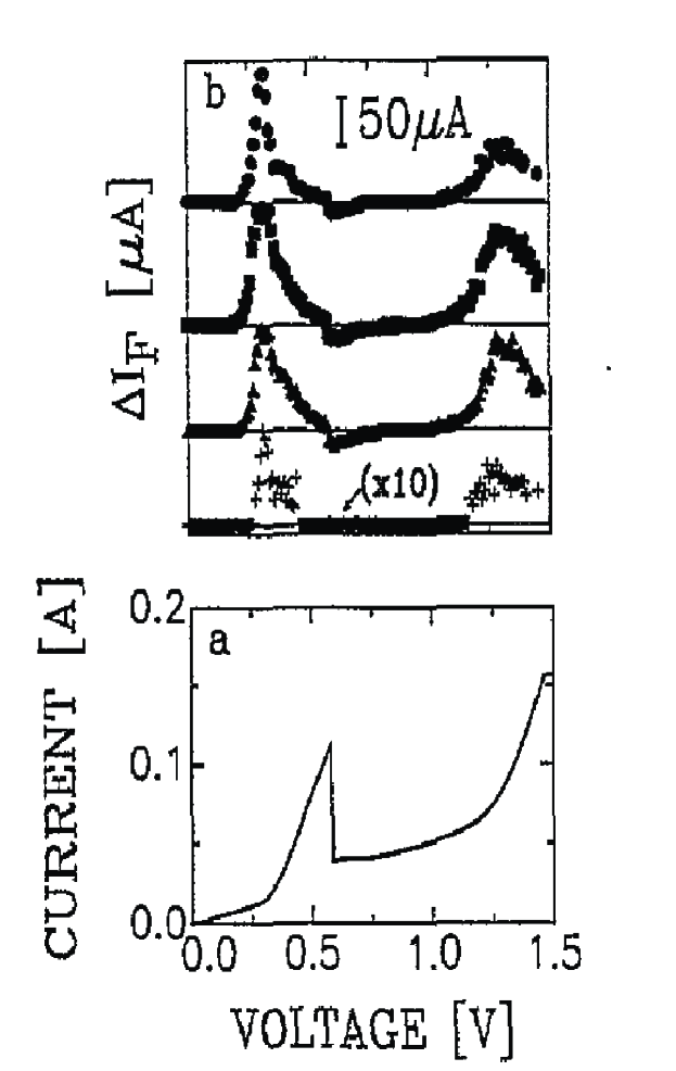
These experimental features could not be reproduced with Tien-Gordon-like models and were related to sample heating. However, careful experiments [86] excluded heating effects in the measured FIR response.
Iñarrea et al [87, 88] showed theoretically that the experiments of Chitta et al can indeed be explained in terms of quantum photon-assisted transport. The crucial point missed in previous theoretical analysis, as we shall describe in the next subsection, is to include the mixing, induced by the photon field, of electronic states with different wave numbers within each spatial region and not only between different regions.
6.1 Transfer matrix description of photoassisted coherent tunneling
As we have mentioned in section 2, theoretical work on tunneling devices under the influence of a time-dependent potential has a long history. After the work of Tien and Gordon[2] on superconducting tunneling devices in microwave cavities, several authors have investigated the effect that external ac potentials have on different sample configurations. Among them, Jonson[91], Johansson [93] Apell and Penn [95] have studied the sequential contribution to the tunneling through a resonant tunneling diode with an applied electromagnetic field, using models based on the TH formalism[7] (see section 6.4). In the spirit of Tien and Gordon, see Eq. (1), most of these works consider that the coupling between electrons and the electromagnetic field takes place just in one region of the structure, the well or the reservoirs, but not in the whole structure.
Iñarrea et al [87] analyzed the coherent transmission coefficient and tunneling current for non-interacting electrons considering that the radiation interacts with barriers, well and contacts. As mentioned in the previous section, the photon field mixes electronic states with different wave numbers within each spatial region. The inclusion of this mixing is crucial in order to explain the experimental evidence. The most popular model for photon-assisted tunneling developed by Tien and Gordon [2] assumes that the interaction with the electromagnetic field can be described as an effective time-dependent potential within each spatial region of the system. Importantly, this model assumes that the potential drop due to the external time-dependent field occurs only between two regions, namely , but not inside each region. This has to be compared with the exact coupling term in the Hamiltonian which, depending on the chosen gauge, is of the form ( is the vector potential of the electromagnetic field and is the electronic momentum operator) or ( is the electric field and is the position operator). These kind of terms produce transitions between different electronic states within each region of the structure (leads and well). In DB’s the coupling of the well states with the continuum states of the contacts produces a quasi-continuum of states in the well such that the transmission coefficient and the tunneling current in the presence of radiation can be strongly modified due to the aforementioned mixing. Thus, a description in terms of the TG model is not suitable for describing photon-assisted tunneling through a DB. However, in systems like multiple quantum wells (where the interwell sequential tunneling through quasidiscrete states determines the tunneling current) the TG model can be applied in most cases.
Following Iñarrea et al, the one-electron Hamiltonian for a double barrier system in the presence of an electromagnetic field (EMF) represented by a plane electromagnetic wave of wave vector , parallel to the direction and polarized in the direction , can be written as:
| (113) |
Where the Hamiltonian is written within the effective mass approximation and is the double barrier potential accross the growth direction, , of the heterostructure (an applied dc bias voltage is included in the definition of ). In the Coulomb gauge , Eq. (113) becomes:
| (114) |
where the vector potential operator is .
In general, is negligible compared to the term, therefore in second quantization the total Hamiltonian becomes:
| (115) | |||||
where
| (116) |
| (117) | |||||
with ( is the photon frequency and the wave vector of the EMF has been neglected). is the independent, electronic Hamiltonian and includes the double barrier potential and the external applied bias voltage. The operators create the eigenstates of , which describe tunneling states for bare electrons (the factor is already included in the state vector ). , is the photon field Hamiltonian whithout coupling with electrons and and , describe the coupling between electrons and photons in the total Hamiltonian.
The coupling term can be divided into the ”diagonal” and the ”off-diagonal” contributions. In these systems a quasi-localized state is connected by the EMF with a continuum of extended states. Therefore , can be treated in first order time dependent perturbation theory. For problems in which two o more quasi-localized states should be connected by the light, the method could not be applied in the same way, requiring some generalization. Therefore, the total Hamiltonian can be written as:
| (118) |
where . The Hamiltonian , can be solved exactly considering a canonical transformation[87, 91]. It allows the exact electronic wave function dressed by photons to be obtained: , where is the electronic double barrier eigenstate with no photon field present in the sample. Once the eigenstates for are obtained, time dependent perturbation theory is applied in order to treat the term. The operator for the canonical transformation is given by , where can be written as:
| (119) | |||||
The Hamiltonian under this transformation becomes:
| (120) |
where and . In the transformed Hamiltonian the electrons and photons are not coupled anymore and the electronic eigenvalues are shifted in which is negligible with respect to the free electron eigenvalues. Assuming a semiclassical EMF, where N is the number of photons171717A classical treatment of the electromagnetic field is justified for the range of field parameters in typical experimental setups. To estimate the number of photons , one can use the relation between intensity, , and field strength, : (for GaAs, and ) together with , namely the relation between the energy content per unit volume, , the photon energy and the number of photons. Solving for , one gets for the experiments of Sollner et al [78] (typical frequencies of 2.5 THz and intensities ) photons in a volume of .. From the above expressions can be written as: . Finally the exact eigenstate for can be expressed in terms of the electric field intensity :
| (121) | |||||
where
| (122) |
Note that the scaling parameter of the Bessel functions characterizing the photonic sidebands depends on the frequency as as compared with the TG model where the dependence goes as . This difference in the scaling parameter has been studied in detail by Wagner and Zwerger in Ref. [40] and indicates that the TG model is not applicable in situations involving ac fields rather than ac potentials.
Once the eigenstate for is obtained, time-dependent perturbation theory is applied in order to treat the term. By doing this, the expression for the total wave function of the tunneling electron under the influence of the EMF becomes:
| (123) |
is the wave vector of the initial electron, is the wave vector of the corresponding electronic coupled states and is a normalization constant. The time dependent coefficients are given by:
| (124) |
where
| (125) |
such that
| (126) |
and run from to and . The normalization constant , guarantees current conservation. is the ”dressed” or diagonal reference state and , represents the coupled ”dressed” states due to photon absorption and emission. The spectral density consists in a central peak (weighted by ) and infinite n-sidebands separated in from the central peak and weighted by . If the argument of the Bessel functions is very small, the sidebands intensities are negligible and it is enough to consider transitions between the main side bands (the ones weighted by ) of different electronic states separated in energy by . For higher values of , the spectral density weight is shared between the satellite peaks and their contribution cannot be neglected. Applying the current operator to the transmitted and incident wave function, the time-averaged coherent transmission coefficient following the Transfer Matrix technique [87] becomes:
| (127) |
Where =1. is the coherent transmission coefficient for a double barrier at the energy corresponding to a wavevector . In the case of very small only one photon absorption and emission processes are considered and:
| (128) |
such that
| (129) | |||||
A similar expression can be obtained for the reflection coefficient replacing , and by , and respectively. , and , (, and ), are the standard coherent double barrier reflection (transmission) coefficients, evaluated at the reference energy, at one photon above and at one photon below the reference energy, respectively.
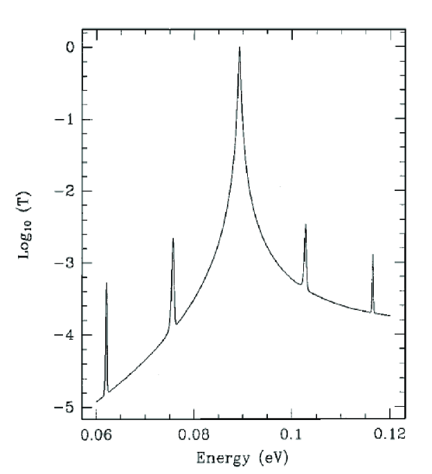
This expression for the reflection coefficient verifies current conservation: , meaning that the probability for an electron to tunnel with no photon absorption or emission is smaller than the corresponding with no light present in the sample which is a consequence of unitarity. As the EMF intensity increases, multiphoton processes play a role in the transmission probability and formula Eq. (127) has to be considered.
Using the above formalism, Iñarrea et al [87, 89] studied the experiments of Chitta et al [3], see Fig. 4. Their results are shown in Fig. 5 where the multiphoton transmission coefficient for coherent tunneling is plotted (field intensity , and zero bias voltage). The main features observed in the transmission coefficient T(E), are multiple satellite peaks at both sides of the central one, coming from photon absorption and emission. The two closest peaks to the central one correspond to one photon processes, mainly to the transitions between the zero-side bands of electronic states differing in one photon energy. The other two peaks separated 2 from the main one correspond to processes involving two photons. Higher multiphoton transitions have much weaker intensities.
In Fig. 6(a) the coherent tunneling current density as a function of the dc voltage in the presence of the FIR laser is plotted. The effect of the light on J can be observed in Fig. 6(b) and Fig. 6(c) corresponding to =13.6 meV and =4.2 meV respectively.
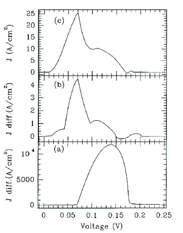
In these figures, the current difference, with and without EMF, , is plotted versus the applied dc bias voltage. One observes firstly that the current threshold takes place at the same voltage for both frequencies. Also, a main peak appears for both cases at the same voltage. This central peak corresponds to the current threshold without light. A shoulder appears for voltages close to the center of the current peak at the higher voltage side, a weak negative contribution shows up for higher bias voltage and, finally, a small structure, associated with the current cutoff, appears. The fact that the current threshold takes place at a lower bias voltage than in the case without radiation is easy to understand: the electrons in the emitter can absorb photons and the current flows when ( is the energy of the resonant state in the well and the Fermi energy at the emitter). On the contrary, the fact that the threshold is frequency-independent is not expected. This counterintuitive behavior (at first sight, one would expect a linear shift with respect to of both the current threshold and the main peak of ) is in qualitative agreement with the experimental results of Fig. 4 [3]. The first attemps made in order to explain these results, first in terms of classical response and secondly relating the experiments to sample heating due to the laser, failed. The dependence of J with the temperature [86] shows a qualitative different behavior than the obtained in the presence of the laser, and, therefore, heating does not explain the experiments (see Fig. 2 and Fig. 3 of Ref. [3]. Regarding to the classical response, the photon energies considered are much larger than the energy broadening of the DB resonant state and a quantum behavior is expected.
The qualitative agreement between the experimental photon-assisted tunneling current and
the transfer matrix calculations by Iñarrea et al [87, 89]
allows to understand the features discussed above. The fact that
the current threshold for different takes place at
practically the same bias voltage is related to the multiphotonic
processes. If one compares the two cases corresponding to
=13.6 meV and = 4.2meV (fixed F) in Fig. 6, it
is obvious that is larger for the smallest frequency, =4.2 meV,
such that more side bands contribute
efficiently to the current. Therefore, the current threshold moves to
a lower bias voltage as compared with cases
where only single photon processes do contribute. These
multiphoton contributions wash out the linear dependence that the
threshold voltage should follow as a function of if
only one photon process took place.
Concerning the main peak in , its frequency-independent position is related with the number
of parallel states available to tunnel resonantly with the
absorption of one or more photons. The main peak corresponds to
the voltage where the resonance energy, , is just above the
Fermi energy, , at the emitter. In this situation the
number of parallel states which can tunnel resonantly via
absorption of
one or more photons is maximum no matter the considered.
6.2 Sequential tunneling current
In the sequential tunneling regime the electrons suffer scattering processes and the electronic wave function looses memory in the quantum well.
The sequential tunneling contribution to the current can be obtained evaluating separately the current for the first and the second barriers, , and . These currents are related to the Fermi level in the well (which defines the amount of electronic charge stored into the well). The Fermi Level is obtained selfconsistently by imposing current conservation, namely . This procedure takes into account the possible scattering processes within the well in a phenomenological way.
In order to calculate , and without light, the TH method [7] should be considered. The probability for the electron to cross from the emitter to the well reads:
| (130) | |||||
where is the transmission coefficient for a single barrier; () and () are the perpendicular (parallel) component for the electronic wave vector in the emitter and well respectively. For a given bias voltage , is the well state energy referred to conduction band bottom: (where , is the well state energy referred to well bottom and , and are the left barrier, well and total widths respectively). Finally, , , where is the width of the right barrier.
For small values of , it is enough to consider one-photon processes only and the sequential current through the left barrier reads:
| (131) | |||||
where the subscript ”0” means the reference state energy that in our case is the resonant well state energy. The subscript ”1” and ”-1” mean one photon energy above and below respectively, and , and are the transmission coefficients through a single barrier, in this case, the emitter one. For the second barrier a similar expression is obtained for .
By using the method above to calculate the sequential contribution to the current, Iñarrea et al conclude in Ref. [87] that the current in the experiments of Chitta et al [3] is mainly given by a coherent contribution. The calculated sequential current is of the same order as the coherent one but the current difference (with and without irradiation) for sequential tunneling is one order of magnitud smaller than the corresponding to the coherent tunneling.
6.3 Magnetotunneling current in the presence of radiation
The analysis of the magnetotunneling current for both configurations of the magnetic field, parallel and perpendicular to the growth direction of an heterostructure, gives a great deal of information on the density of states in the well corresponding to the Landau level (LL) ladder, in the first case and on the edge states in the second configuration [105, 106, 107]. As described in Ref. [98], an external radiation field can be used to widen the information obtained upon the application of a magnetic field.
The coherent magnetotunneling current through a DB when a magnetic field is applied parallel to the current in the presence of light can be analyzed following a similar scheme than the one described in section 6.1. If the FIR radiation is linearly polarized in the same direction as the static magnetic field, the electronic motion is modified by the light only in the transport direction and the electronic lateral states remain unaffected by light. With no magnetic field present, the parallel component for the electronic wave vector is conserved during the coherent tunneling process. In the presence of a magnetic field, it is the LL index what is conserved: the current presents a peak as a function of the external bias voltage when a LL in the emitter aligns with the corresponding one in the well. As the magnetic field increases, the degeneracy of each LL increases, less number of LL contribute to the current and, as a result, the current presents less, but more intense, peaks.
In the presence of FIR radiation, the electronic part of the Hamiltonian in Eq. (115) is modified as:
| (132) |
where is the magnetic field intensity, is the
cyclotron frequency, and are
the creation and destruction operators for the Landau states, and
is the electronic energy perpendicular part.
is the independent
electronic Hamiltonian and includes the double barrier potential
and the external applied bias voltage, therefore the eigenstates of
, , are the tunneling states for bare
electrons in the presence of a magnetic field. The rest of the
terms in the Hamiltonian are as in Eqs. (116-117).
Following the derivation in section 6.1, the coupling term is divided in the
”diagonal” and the ”off-diagonal” contributions:
where . Again, the Hamiltonian
, can be solved exactly by a canonical transformation and
the off-diagonal term is treated in time dependent perturbation
theory.
The expression for the
coherent magnetotunneling current is:
| (133) |
the LL index, is the maximum LL index occupied, and the coherent transmission coefficient through a double barrier structure when the photon field is present in the sample.
An example of the effect of FIR radiation on the coherent magnetocurrent through a DB is plotted in Fig. 7(a), where the coherent magnetocurrent density is represented as a function of the external bias voltage.
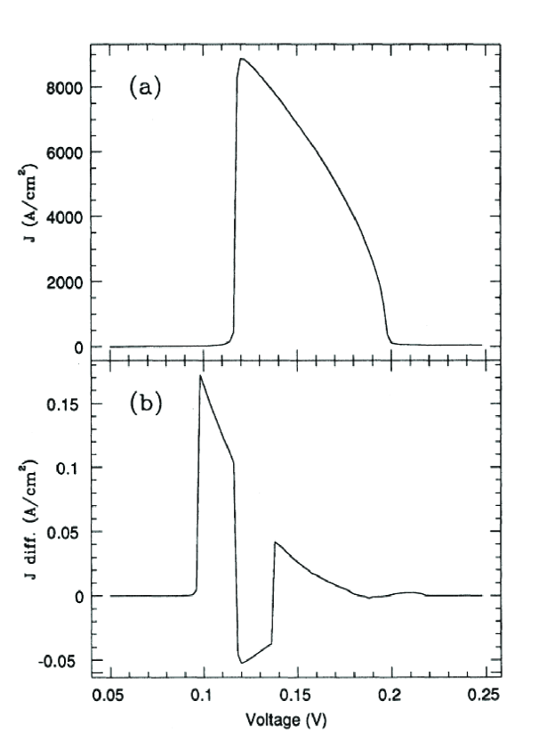
In this case, only one LL contributes to the tunneling current and the analysis of the effect of the light on the current can be done in a simpler way than in the case where more LL participate in the current.
The current difference, with and without light, is plotted in Fig. 7(b). In this case there is a main peak which appears for smaller bias voltage than the corresponding to the threshold bias voltage for the magnetotunneling current with no light present. As increases the current difference decreases and becomes negative. There is also a small positive and a negative structure for higher voltages and as the voltage corresponding to the cut off of the current is reached there is an additional positive contribution to the current difference. These features are schematically explained in Fig. 8: for small voltages the resonant state in the well with energy corresponding to the first LL is higher in energy than the Fermi energy in the emitter.
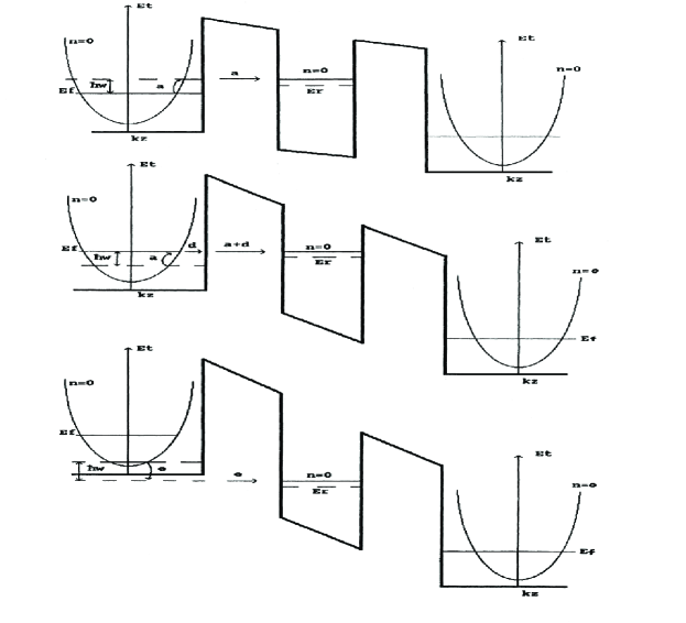
As the voltage increases there are electrons close to which are able to absorb a photon and tunnel resonantly from the first LL in the emitter with LL index conservation, therefore the threshold voltage for the current is smaller than the corresponding one for no light present (it moves twice the photon energy) and there is a positive peak in the current difference. For higher voltages the first LL in the well crosses the in the emitter and the current difference becomes negative abruptly due to the fact that the electrons in the emitter have the possibility to absorb a photon and it reduces the number of electrons efficient to tunnel resonantly. For higher voltages there are absorption, emission and direct tunneling processes whose combinations give the positive structure observed.
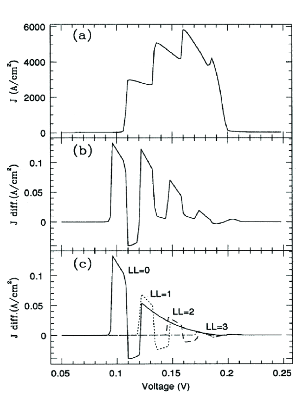
As increases and the energy of the resonant state in the well for the first LL lies one photon higher than the conduction band bottom of the emitter the electrons have a probability to emit a photon below the bottom of the conduction band and the resonant current is reduced (it corresponds to the small negative contribution to the current difference for large voltages). Once the resonant state crosses the bottom of the conduction band there are electrons in the emitter which can emit a photon and tunnel resonantly, therefore there is a positive peak in the current difference and the current cut off moves to larger voltages.
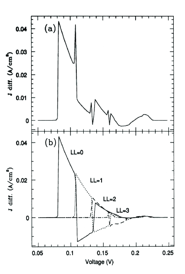
As the magnetic field decreases there are more LL s which contribute coherently to J. In Fig. 9(a) the current as a function of the external dc bias voltage is plotted for a field of 8 Tesla. We observe four LL s which contribute to J. The photon frequency is 6.9 meV (one half of the cyclotron frequency ). The current difference is shown in Fig. 9(b). In this case the main peak in the current difference due to the effect of the light appears at different bias voltage for the different LL s and the contribution at the cut off is added up for the four levels. In Fig. 9(b) the current difference has been plotted separately for each LL. If the photon frequency is tuned to the same value as the cyclotron one for the same magnetic field (8T) the current difference changes dramatically and the main contribution comes from the peak at the threshold bias voltage and an additional narrow structure in this region of voltages (Fig. 10). For higher voltages the additional features to the current difference are much smaller in intensity than in the previous case. The reason for this difference between both cases is not only the change of the threshold voltage and cut off of J due to the difference of photon frequencies (the threshold voltage is lower for higher photon frequencies and the cut off voltage is larger for higher photon frequencies) but also is due to the fact that when the ratio is one, there are absorption and emission processes taking place for electrons coming from different LL s which compensate each other. This feature can be observed in Fig. 10(b), where the contribution to the current density coming from each LL is represented. Due to this compensation it is possible to control the the effect of the light on the magnetocurrent by tuning the ratio between the cyclotron and the photon frequency.
The sequential magnetotunneling current for the same cases as the coherent one was evaluated in Ref. [98].
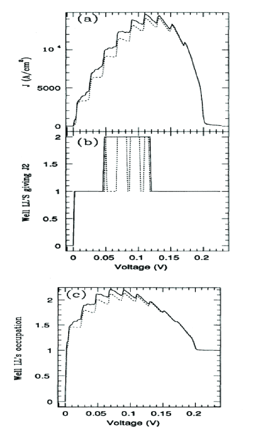
Again, the calculated sequential current is of the same order as the coherent one but the current difference (with and without irradiation) for sequential tunneling is much smaller than the corresponding to coherent magnetotunneling. When the frequency of the applied laser () equals the cyclotron frequency, there are compensations in the current difference coming from different LL s and the light affects mainly the current density at the threshold and the cut off voltage.
The LL index, which is conserved if tunneling occurs coherently, is not conserved for sequential tunneling. When an electron tunnels through the first barrier, inmediately relaxes inside the quantum well and, thus, looses information about the LL index carried during the tunneling event. Therefore, the number of LL s at the emitter contributing to the current can be different than the ones participating in the tunneling current from the well to the collector. Interestingly, these numbers can be modified by the external radiation. An example is shown in Fig. 11, where at low field (6T) there are many Landau levels giving current. The dotted line represents the magnetocurrent when no light is present and the continuous line corresponds to the case where the sample is irradiated ( and ). Without radiation, the current presents a sawtooth profile coming from the participation of additional LL’s as the bias voltage increases. When the light is switched on, the current threshold moves to lower voltages and there is a three step like structure between each jump.
The total number of LL s partially occupied in the well (as a function of the bias voltage) are represented for both cases in Fig. 11(b): with (continuous line) and without (dotted line) light. For values of the second LL begins to be occupied in the irradiated case. Without light, the second LL level begins to contribute to the current through the second barrier at a slightly larger voltage. As increases, the well is discharged and the second LL becomes empty for the case in which there is no light present. Finally, at large voltages, the bias voltage at which the second LL becomes discharged is smaller in the case whitout light than in the irradiated case.
6.4 The Transfer Hamiltonian method for photon assisted tunneling: some examples
The TH formalism is suitable to study systems with localized states (for instance to analyze the effect of an external magnetic field parallel to the interfaces of the heterostructure, where the edge states are the electronic eigenstates) and situations where external fields, scattering proccesses or other perturbations affect in different way the different spatial regions of the system.
Jonson investigated inelastic resonant tunneling in the presence of a boson field by means of the TH method [91]. Within this approach, the Hamiltonian describing tunneling from the left reservoir to the well is181818Along this discussion we consider non interacting electrons.:
| (134) |
where
| (135) |
It is assumed that the boson energy has no dispersion and that the electron-boson interaction takes place only in the quantum well (with only one resonant level). The wave vector is decomposed in a component perpendicular to the heterostructure and a parallel component , namely , such that: .
Within the TH formalism the tunneling current through the barrier is obtained from the rate of change of the number operator for electrons in the left reservoir, namely , as . By using it can be shown that the current reads (see also Section 5):
| (136) | |||||
A similar description holds for the current . In Eq. (136), is the equilibrium (Fermi-Dirac) distribution function of electrons the left reservoir and is the distribution function of electrons inside the well. If some scattering mechanism inside the well is implicitly assumed in order to maintain thermal equilibrium, is a Fermi-Dirac distribution function and has to be calculated by imposing current conservation
| (137) |
If, on the other hand, resonant tunneling occurs without any scattering, itself has to be calculated by imposing current conservation
| (138) |
and a nonequilibrium distribution function is obtained.
Moreover, the current depends on the product of the two spectral functions and . Due to the coupling to the bosons, the spectral function in the well changes from the delta-function form to a more complicated function involving a distribution of free-electron spectral functions191919This can be shown by considering the canonical tranformation with , see also Eq. (119) in section 6.:
| (139) |
where the strenght is given by:
| (140) |
In Eq. (140) is a modified Bessel function, is the adimensional coupling
| (141) |
and is the Bose-Einstein distribution function .
Jonson applied the above model to study photoassisted tunneling through resonant devices. By treating the photon field semiclassically (see footnote 17), one recovers a model similar to the Tien and Gordon model [91].
Foden and Whitaker presented in Ref. [108] a quantum electrodynamic treatment of photon-assisted sidebands that appear when an electron tunnels through a resonant state and interacts with a coherent field, namely a Hamiltonian of the form:
| (142) |
where . Again, the electron-photon coupling is assumed to take place only in the quantum well. The photon field is described by a single-mode coherent state , namely a Poisson distribution of number states with mean value (the expectation value of the electric field in this state is ). Considering just one resonant state, they obtained the quantum well spectral density:
| (143) |
with and . Under the influence of radiation, the spectral function is shifted by due to the renormalization of the electron energy as a result of its interaction with the electromagnetic field, and splits in a series of side bands. This result differs from the one obtained from a semiclassical model (see Eq. (4)):
| (144) |
In the quantum case the relative intensities of the spectral lines are different from those obtained classically and the spectrum becomes asymmetric with respect to the line [108]. This can be understood in terms of spontaneous emission of photons by the electron due to the interaction with the vacuum fluctuations of the electromagnetic field. This asymmetry is, of course, not present in the clasical limit.
Johansson analyzed in Ref. [93] the effect of an ac component in the voltage across a double barrier. The ac voltage is included only in the reservoirs as:
| (145) |
and the quantum well (with a single resonant state) is assumed to remain unafected by the time dependent field. By using the TH method to calculate the transmission probability for incoming electrons, Johansson concludes that when the period of the ac voltage is short compared with the lifetime of an electron inside the quantum well, photon-assisted tunneling occurs. If, on the other hand, the period is long the transmission probability is governed by the instantaneous value of the voltage. The effect of interlevel transitions due to the coupling with radiation was considered by Johansson and Wendin in Ref. [96]. They reported shifts of the positions of the transmission resonances due to the Dynamic Stark effect.
All the treatments above consider the coupling with the external field just in one part of the structure. In particular, neglecting the effects of the field outside the quantum well is only a good approximation as long as the frequency of the field is higher than the plasma frequency of the electron gas in the doped contacts. When this is not true, the electrons in the contacts screen the external field strongly and most of the interaction between the field and tunneling electrons will take place outside the well. Above the plasma frequency, on the other hand, most of the absorption and emmission of radiation by the tunneling electrons occur when they are in the quantum well. For an electron gas in GaAs with Fermi Energy of 50 meV the plasma frequency is of the order of 40 meV. The plasma frequency increases with increasing Fermi energy roughly as [95]. Usually, in experimental setups for resonant tunneling diodes the Fermi energy at the contacts is around 50 meV and the photon frequency is of the order of 10 meV. In order to compare with available experiments in these systems, it is thus crucial to include the coupling of the radiation with the contacts, as we have described in section 6.1.
6.5 Generalized Transfer Hamiltonian for coherent photon assisted tunneling
The Transfer Matrix technique described in Sections 4.1 and 6 is a very powerful tool to analyze coherent tunneling. Here, we review an alternative method. This method, which generalizes the TH approach we have described in Section 6.4, accounts for high order tunneling events (beyond the first order described by the TH).
The extension of the TH method was put forward by Brey et al in Ref. [109] to the study of tunneling through resonant states in heterostructures. The method, dubbed generalized Transfer Hamiltonian (GTH), allows to describe not only the sequential tunneling (which considers the electrons tunneling through each single barrier in a sequential way) but the coherent one which includes the virtual transitions through the resonant states for electrons crossing coherently the system. The GTH was later extended by Aguado et al in Refs. [99, 100] to include the effect of ac potentials using the two configurations discussed along this section: constant potentials (no mixing of electronic states, case a) and a coupling of the form (mixing of electronic states, case b).
The TH considers a localized basis representation, namely approximated Hamiltonians whose eigenstates are spatially localized (see and in Fig. 12(a). By means of the interaction picture the required perturbations are switched on adiabatically:
| (146) |
Where and are sketched in Fig. 12(b).
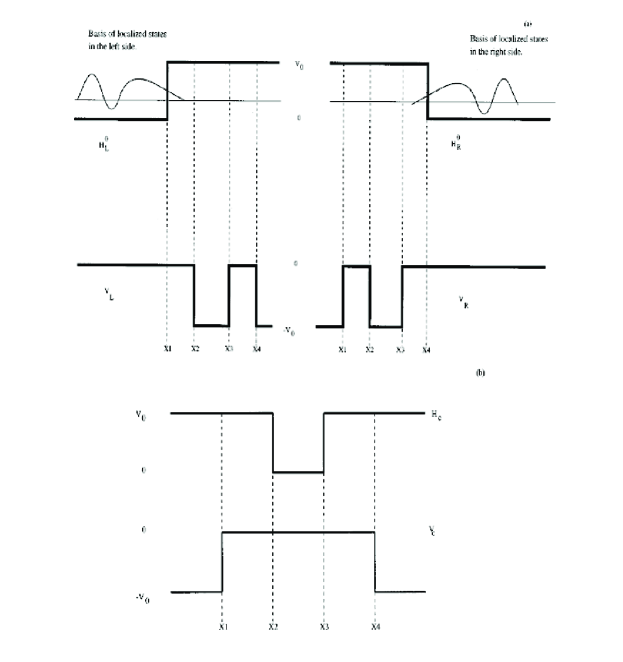
Following Aguado et al in Ref. [99], the time evolution of the wave function, including ac potentials (case a) of the form , see Eq. (145), on both sides (left and right), can be written as:
| (147) | |||||
This wave function must describe a particle initially on the left side. This is satisfied by taking and . The electrons in a particular state can in principle evolve to any state in the right side so that a summation over right states is required in the expression of the wave function. The time evolution operator gives the evolution of an electron to a right state and is determined at every order from the Schrödinger equation by an expansion in a perturbation series. becomes in terms of the retarded Green’s function:
| (148) |
where
| (149) |
The transition probability from left to right per unit time can be expressed as , where includes the sum over all orders in perturbation theory.
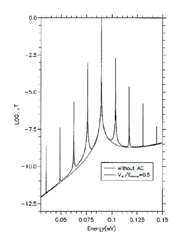
Performing the summation and taking the stationary limit, the expression for the transition probability reads:
| (150) | |||||
Where is the total retarded Green’s function of the system
| (151) |
This formula for the transition probability is a natural extension of the Fermi Golden Rule formula [91, 93, 95]. The first term corresponds to first order perturbation theory, and is the only one appearing in the TH method [7]. The term containing the retarded Green’s function is the one which includes processes which involve intermediate states and therefore describes correctly the coherent resonant tunneling.
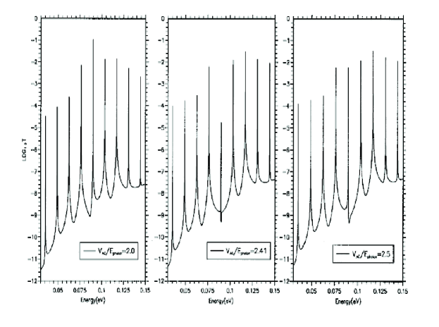
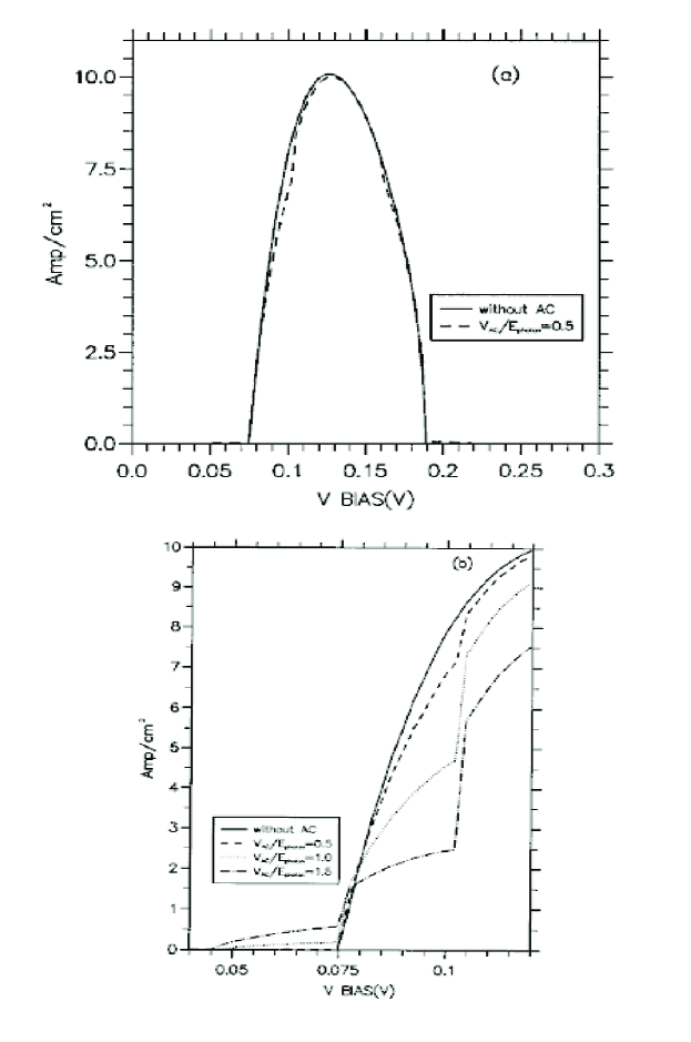
The transmission coefficient through the structure can be calculated from Eq. (150). An example is shown in Fig. 13. In this case, processes up to fourth order contribute to the transmission as reflected in the four satellites which appear at both sides of the main central peak. Note that the broadening of the resonant states in the well is not a constant but depends on the side band index [99]. In the present case the contribution of the photoside band of index 0 to the transmission coefficient is smaller than the one coming from the main peak (m=0). In Fig. 14 an example of dynamical localization is shown.
The current through a double barrier versus the applied bias voltage is plotted in Fig. 15 for different parameters of the ac potential. The main features are: a shift of the threshold current to lower voltages and the reduction of the current for larger voltages in the presence of the ac potential. This effect increases as the ratio increases. Also a step-like behavior is observed (see Fig. 15(b)). These features can be explained in terms of the photoside bands. The contribution to the current at low dc voltages comes from photoside bands associated to electronic states close to the Fermi energy in the emitter. They contribute to the resonant tunneling when the resonant state is above , , via the absorption of photons. This process has a low spectral weight and its contribution to the current is small. By increasing the applied dc voltage, approaches such that another photo-sideband corresponding to the process () starts to contribute. The spectral weight corresponding to this process is higher and the current increases. The reduction of current (with respect to the case without ac) can be explained similarly in terms of the photo-sidebands.
As discussed in section 6.1, the effect of an homogeneous EMF affecting the whole sample is quite different from the one obtained from spatially constant ac potentials. Including the EMF within the GTH scheme in a similar fashion as the one described by Eqs. (116-117), the transition probability (only one photon processes are considered) for this second configuration (case b) can be written as [99]:
| (152) | |||||
where and contain the matrix elements:
| (153) | |||||
where is the total Green’s function and
| (154) |
In these expressions, the argument of the Bessel functions is now governed by matrix elements of the momentum operator, cf. Eq. (122). An example of the comparison between cases (a) and (b) is shown in Fig. 16 where the transmission coefficient is plotted for both configurations. Typically, the argument of the Bessel functions of high order are negligible in the second case (the momentum matrix elements are very small) such that only two satellites show up in the transmission coefficient Fig. 16(b). Furthermore, these side-peaks have another origin than the photoside bands of Fig. 16(a): they come from the mixing of electronic states due to the homogeneous light, namely they appear from the off-diagonal matrix elements of the electronic momentum coupled by the light.
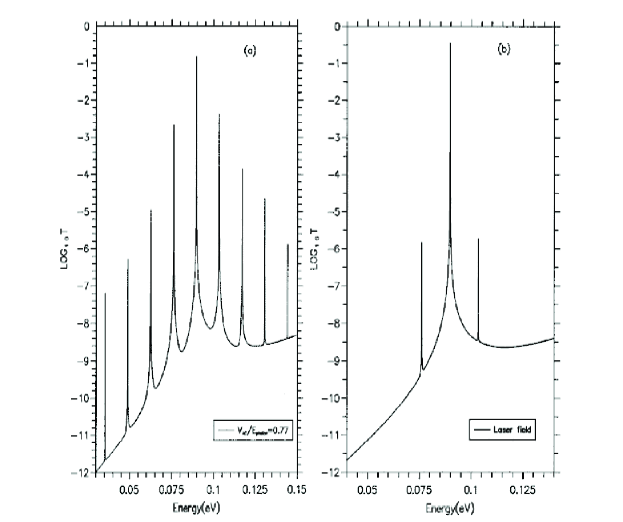
In other words, the tunneling channels for the two configurations are different. In the case of an ac potential the off-diagonal terms cancel if the time dependent field is considered constant within each region (left, center and right). In this case, the main tunneling channels (the only ones within this approximation) are the photoside bands: those in the emitter align in energy with the photoside bands in the well producing additional contributions to the transmission probability and the resonant current. Their contribution can be important even for high order photoside bands if the ratio . In the case of homogeneous light, the situation is different. The off-diagonal electron-photon coupling terms in the Hamiltonian are the ones which modify the transmission and, thus, the current. These channels, involving different electronic states, Fig. 16, contribute in principle also with all their photoside bands. However, since the argument of the Bessel functions, which is controlled by the momentum matrix elements (see Eq. 122), remains very small, just the zero index photoside band (the main one) is non-negligible and gives a contribution to the transmission. Therefore the three peaks in the transmission coefficient come from the main bands (index zero) corresponding to three electronic states which differ in one photon energy and which are mixed by the EMF field.
6.6 Beyond the single electron picture: charge accumulation effects and current bistability
So far, we have discussed photon-assisted tunneling of independent electrons. The effect of the electrostatic fields induced by the electronic charge are not considered in the model calculations of sections 6.1-6.5. The space charge alters the voltage distribution over the whole structure such that the actual electrostatic potential profile does not correspond to the simple description in terms of abrupt interfaces. One consequence of that is the appearance of intrinsic current bistability, two values of the current for a given dc bias voltage, which is caused by the electrostatic feedback of the space charge dynamically stored in the well.
The first experimental evidence of intrinsic current bistability in the electronic transport through DB’s was observed by Goldman et al in Ref. [74, 75]. Although these experimental results were first questioned in Refs. [110, 111], intrinsic bistability in the current through resonant tunneling diodes was unambiguosly confirmed in subsequent experiments [112, 113, 114]. On the theory side, many papers have been devoted to the study of current bistability in resonant tunneling diodes [75, 77, 115, 116, 117, 118, 119, 120].
6.6.1 Selfconsistent model
As we mentioned, the Coulomb interaction between electrons induces electrostatic fields which modify the distribution of the electrostatic potential through the heterostructure. Therefore, the energy of the resonant states in the quantum well is modified and so the current density for a given bias voltage changes. In a resonant tunneling diode there are three regions spatially separated: emitter, well and collector, where the charge is accumulated. The potential profile through the whole heterostructure is not abrupt and accumulation and depletion layers in the emitter and collector are built up. By solving simultaneously the Poisson and Schrödinger equations these potential profiles, together with the current, can be obtained. This procedure can be simplified by assuming that the accumulated charge in each region is distributed as a two dimensional sheet of charge [75, 121] as we shall describe below.
Assuming that the electrons in the well are in local equilibrium with Fermi energy which define the electronic density , current conservation can be used to obtain the Fermi energy in the well as:
| (155) |
with the (zero-temperature) currents:
| (156) |
is the half-width of the resonant level and the rest of parameters are defined as in subsection 6.2. In Eqs. (155), denotes the set of voltage drops through the structure. The Poisson equation yields the potential drops in the barriers, and , and in the well, :
| (157) | |||||
| (158) |
where is the GaAs static permittivity, is the 2D (areal) charge density at the well (to be determined), and are the well and barrier thickness respectively, and is the 2D intentional doping at the wells. The emitter and collector layers can be described by the following equations [74, 121]:
| (159) |
| (160) |
To write the emitter equations (159), we assume that there are no charges in the emitter barrier. Then the electric field across (see Fig.26 in section 7) is equal to that in the emitter barrier. Furthermore, the areal charge density required to create this electric field is provided by the emitter. is the density of states at the emitter . To write the collector equations (160), it is assumed that the region of length in the collector is completely depleted of electrons and local charge neutrality in the region of length between the end of the depletion layer and the collector holds.
In order to close the set of equations, two extra equations are employed. The first one imposes global charge conservation:
| (161) |
Finally, all voltage drops across the different regions must add up to the applied bias voltage:
| (162) |
Note that the right hand side of Eq.(161) is the positive 2D charge density depleted in the collector region.
This system of equations, together with appropriate initial conditions, determine completely and self-consistently the current. The generalization of the selfconsistent method to treat multiple-quantum well structures was done in Ref. [122] and will be described in more detail in section 7.
As we mentioned at the beginning of the section, charge accumulation may lead to current bistability in resonant tunneling diodes. An example is shown in Fig. 17 (top), where the charge accumulated (continuous line) in a 50Å-50Å-50Å DB is plotted versus the applied bias voltage. Both directions of the bias voltage, forward and backward, are shown. For comparison, the charge without Coulomb interaction (dotted line) is also plotted.
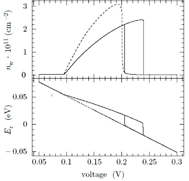
The selfconsistent curve (solid line) presents a clear bistable region around in contrast with the non interacting electrons case (dotted line). The accumulated charge into the well is of the order of . This large value is responsible for the highly non linear distribution of the electrostatic potentials through the structure which eventually produces current bistability. These features can be easily understood by analysing the voltage dependence of the resonant state (Fig. 17, bottom). As expected, the resonant state in the non interacting case (dotted line) drops linearly with . The selfconsistent solution strongly deviates from a linear behavior as soon as charge accumulates in the well. This charge accumulation produces the electrostatic fields which are responsible of the non-linear behavior of . The linear dependence is recovered as soon as the well is discharged. This happens for different voltages in the forward and backward directions leading to bistability.
6.6.2 Current bistability in the presence of light
Iñarrea et al demonstrated in Ref. [121] that the application of an external EMF field modifies the intrinsic bistability properties of a resonant tunneling diode. In particular, the external time-dependent field induces new bistable regions. Furthermore, the bistability region of the unirradiated sample becomes reduced in the presence of radiation. This latter effect has been recently confirmed by Orellana et al [123].
An example of the effects of an external EMF on bistability is shown in Fig. 18(a) where the current with (dotted line) and without (solid line) radiation is plotted versus the applied voltage. The results are obtained along the lines presented in section 6.2 together with the selfconsistent method defined by Eqs. (157)-(162).
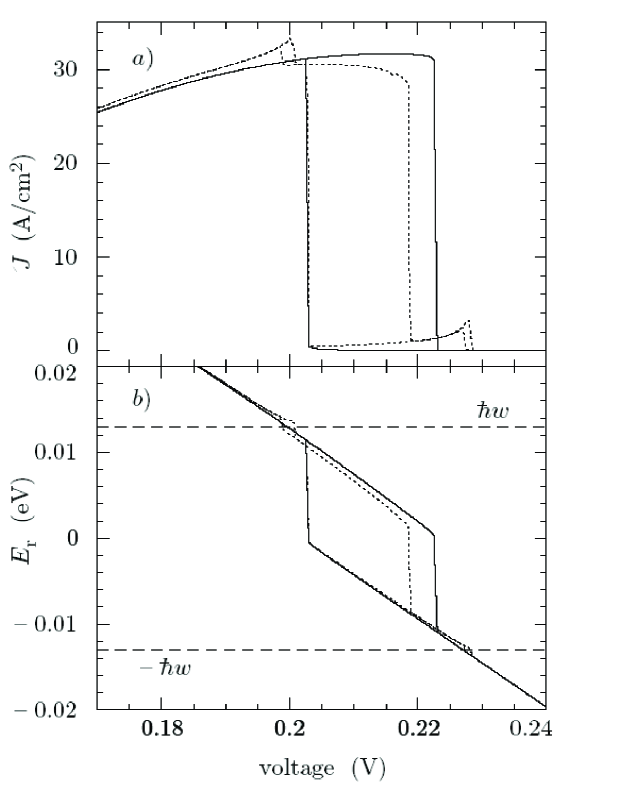
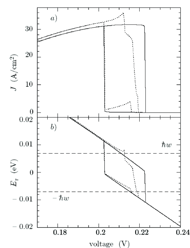
The new bistable regions can be understood by analyzing the voltage dependence of the resonant state (Fig. 18(b)): The possibility of exchanging photons with the EMF field changes the voltage positions at which the the quantum well becomes charged and discharged. The two new bistable regions thus correspond to absorption and emission of one photon. For instance, if is one photon above the bottom of the emitter conduction band, the electrons have a finite probability of emitting a photon below the conduction band and then the light acts discharging the well and so drops abruptly as increases. This effect only occurs in the presence of light and explains the first peak in the current and the first bistability region. Further application of (forward) voltage in the region which corresponds to the resonant state above the emitter conduction band and below one photon energy gives a contribution to the current smaller than the values obtained without light. The reason being again the decrease of the charge density due to the emission of one photon for . As a consequence, the strong non linear effect of the charge on the electrostatic potentials moves below the bottom of the emitter conduction band and the current decreases abruptly at a voltage which is smaller than the one corresponding to the case without EMF. Then, in the presence of light, drops abruptly to a value in the range . Without EMF, the current should drop to zero by energy and momentum conservation if . Increasing further, becomes smaller than and, thus, the current drops to zero. In the backward direction, the current begins to flow at a different voltage than the one corresponding to the current cut off in forward bias voltage which results in a new bistability region. The other bistable regions can be explained similarly.
At lower frequencies, the main bistable region can be also modified as shown in Fig. 19.
6.7 Dynamical selfconsistency for ac-driven resonant tunneling diodes
Noninteracting models assume that the driving field is known and equals the external field.
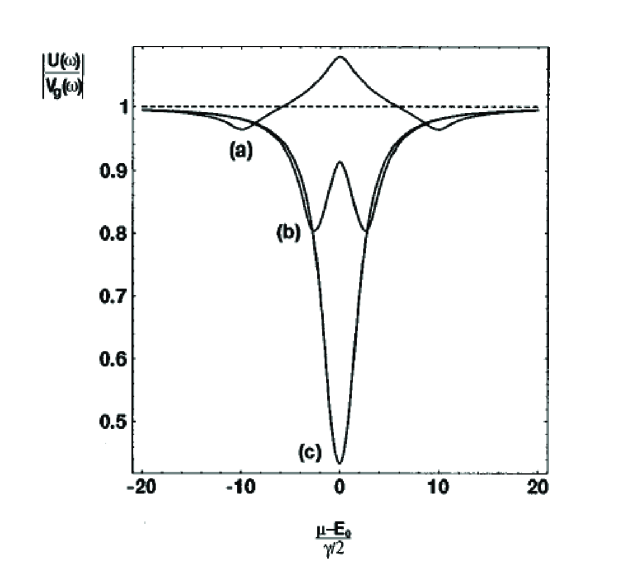
However, the long-range Coulomb interaction will screen the external field and generates an internal potential that deviates considerably from the applied one. We have discussed in Section 6.6.1 how to calculate the internal field selfconsistently by solving rate equations together with Poisson equations. Importantly, the selfconsistent model of Section 6.6.1 assumes that only time-averaged quantities do play a role in order to study stationary transport. This is a simplification: the selfconsistent effect of displacement currents on the internal field can be relevant for some ranges of frequencies. This is of most relevance when treating time-dependent problems.
The theory of frequency-dependent transport in which all frequency components of the current are treated selfconsistently has been put forward by Büttiker and coworkers in a series of papers [47, 45, 124, 125, 126, 127]. Based on the scattering formalism, the analysis of linear ac-conduction in response to oscillating potentials and considering the long-range Coulomb interaction has been discussed in Refs. [47, 124] for zero-dimensional systems and in Refs. [125, 126] for extended systems. The generalization of the scattering formalism to include the nonlinear dependence on oscillating potentials was put forward by Pedersen and Büttiker in Ref. [45].
Here, we briefly describe their selfconsistent calculation for a resonant tunneling diode capacitively coupled to a gate with capacitance [45]. The effect of screening is taken into account to second order in the oscillating potentials by using a random phase approximation (RPA) treatment. Assuming a sample subject to a dc bias and an oscillating voltage applied only to the gate, Pedersen and Büttiker find that the ratio of the applied to the external potential is determined by the ac-conductances :
| (163) |
The ac-conductances read at zero temperature [127, 128]:
| (164) | |||||
| (165) |
The ratio in Eq. (163) has two simple limits. In the non-interacting limit , the internal potential directly follows the applied potential. In the limit , the sample is charge neutral and .
An example of the behavior of as a function of the Fermi energy is shown in Fig. 20 for different frequencies. When the Fermi energy is close to resonance, screening induces a large renormalization of the internal potential. This is expected because at resonance there are more screening electrons. For a given Fermi energy, the ratio changes considerably as a function of frequency. Away from resonance, the ratio converges to the nonscreened case.
Since screening depends on the position of the resonant level compared to the Fermi level, the central peak and the sidebands will experience a different degree of screening and, thus, their intensity will no longer be given by a Bessel function behavior (Tien-Gordon model).
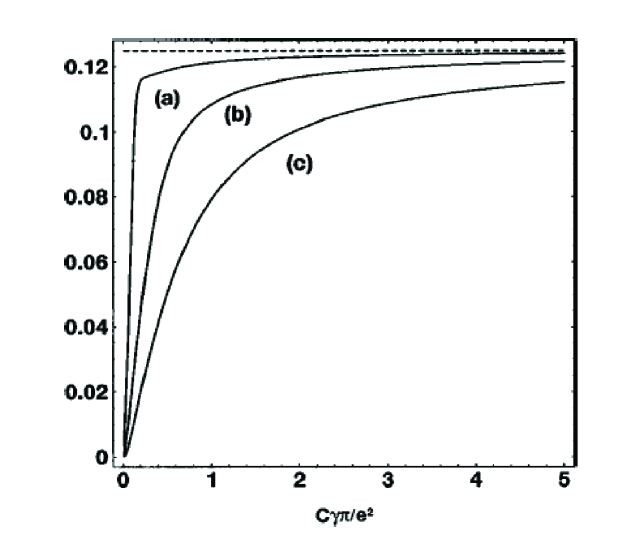
This is similar to the effect described in Section 6.6.1 where the selfconsistent field changes considerably as the quantum well becomes charged. Here, the frequency dependence is also included so one can expect that the ratio of the sideband weight to the central resonance should be frequency dependent. This is demonstrated in Fig. 21 [45]. where the ratio of the sideband peak to the central peak is plotted. The non-interacting theory predicts a ratio of 0.125 for the parameters chosen (dashed line). Depending on capacitance and frequency, the ratio changes completely. Again, as the noninteracting limit is reached and the Tien and Gordon answer is recovered.
The asymmetry between the sidebands is another manifestation of the effects of screening on photon-assisted tunneling.
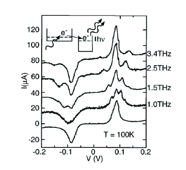
When the Fermi energy if off resonance, emission and absorption of photons occur at different potentials and, therefore, screening will occur asymmetrically for the two peaks. This effect has been observed in photon-assisted tunneling experiments by Drexler et al [129] performed on triple barrier resonant tunneling diodes. An example is shown in Fig 22 where the asymmetry between emission and absorption sidebands is clearly seen. A detailed selfconsistent analysis of these experiments can be found in Ref. [130].
7 ac-driven superlattices
The first unambiguous evidence of discrete photon exchange coming from photon assisted tunneling in a semiconductor structure was obtained by Guimarães et al [133] who studied the current-voltage characteristics of a GaAs/AlGaAs superlattice under intense THz irradiation from a free-electron laser. These pioneer experiments performed at the University of Santa Barbara were followed up by a series of studies [4, 134, 135] were different interesting phenomena like absolute negative conductance or photon assisted electric field domains were observed in the transport through THz irradiated superlattices. In this section we describe some of these phenomena and explain the basic physics behind them.
7.1 THz irradiated superlattices in the linear regime
One of the most spectacular manifestations of photon assisted tunneling in a semiconductor superlattice is the possibility of obtaining absolute negative conductance (ANC), namely a net negative dc current in a sample biased by a positive dc voltage. An example is shown in Fig. 23 [135] where the current at low dc bias voltages is plotted for different intensities of the external THz source (). As the intensity increases, the conductance near zero bias voltage is progressively reduced to zero and, at the highest intensity of the external THz radiation, to absolute negative values. At the same time, several features, not present in the unirradiated curves, start to develop at large voltages. The position of these new peaks are intensity independent and shift linearly with the applied frequency (not shown), unambiguously demonstrating photon-assisted tunneling.
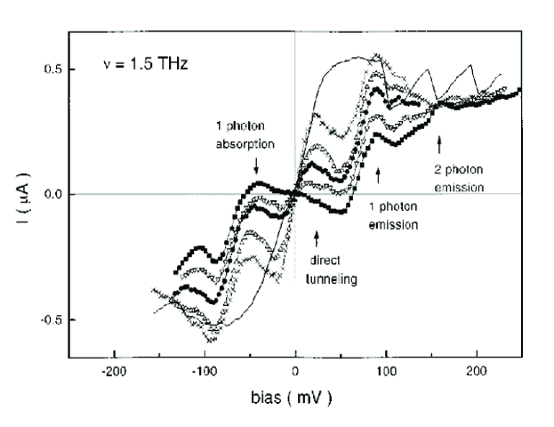
The explanation for this effect is schematically described in Fig. 24: Absolute negative conductance occurs near the condition for dynamical localization. As we described in Section 3, this phenomenon consists in the complete quenching of the direct tunneling channel when the frequency and intensity of the ac field are such that the first zero of is reached. In this case, transport can only occur via absorption or emission of photons. If there is a mechanism that breaks the symmetry between absorption and emission, like broadening of the resonant levels due to, e.g., disorder, it is possible for an electron to absorb a photon an flow opposite to the applied dc bias voltage. This mechanism for ANC is confirmed in more elaborated calculations like the ones presented in Refs. [100, 136, 137, 138, 139]. An example from Ref. [138] is shown in Fig. 25 where a calculation of the current through a superlattice consisting of 10 undoped wells of GaAs wide and 11 barriers of AlGaAs of thickness is presented. Scattering effects are included phenomenologically by asuming that the spectral functions in the wells are Lorentzians whose half width, , is a parameter of the model. It is assumed that the electrons in each well are in local equilibrium with Fermi energies which define the electronic densities . For a given set the densities evolve according to rate equations (for wells):
| (166) |
The interwell currents are calculated within the Transfer Hamiltonian framework (in the sequential tunneling regime). In the presence of the external field, the levels in each well change as ( is approximated for the mean position in the -th well, is the field frequency and F its intensity) such that the local spectral functions in each well are modified by the ac field as in the Tien-Gordon model [138, 139]. The dc current and the final set of densities and Fermi levels is obtained by taking the stationary limit of Eqs. (166). Fig. 25(a) shows the current-voltage characteristics in the region of low bias voltages (without and with external irradiation) for fixed external frequency and different field intensities . The low bias voltage peak in the curve without irradiation (solid line) corresponds to the ground to ground state tunnel between the wells. Once the ac field is applied, the current at low bias voltages is strongly reduced and becomes negative for (dashed line). As the voltage increases further it becomes positive again. For higher intensities (, dotted line), the current is always positive. At a fixed voltage, the negative current occurs as a result of the intriguing interplay between the final local Fermi level in each well, the scattering induced broadening of the density of states and dynamical localization.
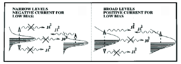
For this structure the dynamical localization condition is reached for such that the current is inhibited through the central channel. This channel is open again increasing F as one can see for F=.
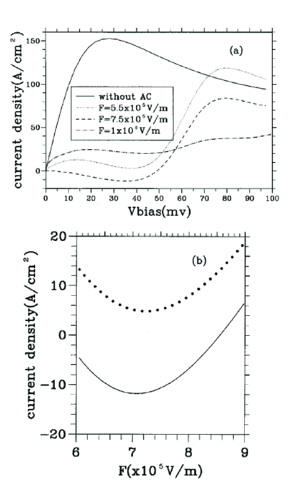
This mechanism for ANC is further substantiated by studying the current at fixed dc voltage for different scattering times. This is shown in Fig. 25(b) [138] where the current at a fixed voltage is plotted versus the intensity of the external field for and two different . For , ANC can occur for some values of , the electrons are able to overcome the static voltage () and electronic pumping in the opposite direction occurs. The current presents a minimum exactly at the first zero of , i.e. . As increases (2meV in Fig. 25(b)) the emission channel is opened i.e., there are empty available states in the next well to tunnel and the flow of current occurs in the direction of the applied dc voltage.
So far, we have restricted ourselves to describe the effect of an external high frequency field in the linear transport properties of semiconductor superlattices. By increasing the dc voltage, charge accumulation in the wells typically occurs and, as a consequence, new phenomena arising from the strong nonlinearity of the problem do start to play a role. As an example, the unirradiated current-voltage characteristics of the experiments in Fig. 23 develops a sawtooth structure reflecting the formation of electric field domains (EFD). The electric field domains develop a complicated structure in the presence of radiation. A description of transport beyond the single-particle picture is thus called for in order to explain these, and others, nonlinear phenomena.
7.2 Weakly-coupled Superlattices as a paradigm of a nonlinear dynamical system I: statics in the undriven case
As we just mentioned, the large dc voltage transport regime in semiconductor superlattices is typically accompanied by strong nonlinear effects. This is expected, because solid state electronic devices presenting negative differential conductance (NDC), such as resonant tunneling diodes, Gunn diodes or Josephson junctions [140], are nonlinear dynamical systems with many degrees of freedom. Semiconductor superlattices display typical nonlinear phenomena such as multistability, oscillations, pattern formation or bifurcation to chaos, all these nonlinear phenomena have their origin in the interplay between Coulomb interaction and NDC. In this section we briefly describe the static and dynamical transport properties of biased heterostructures whose main mechanism is sequential tunneling. This is a topic which has attracted a great deal of attention in recent times. In n-doped weakly coupled superlattices, multistability due to domain formation has been much studied both theoretically and experimentally, [141, 142, 143, 144, 145, 146]. When the doping in the wells is reduced, self-sustained current oscillations [147, 148, 149, 150, 151] and chaos [152, 153, 154, 155, 156] due to domain dynamics are possible.
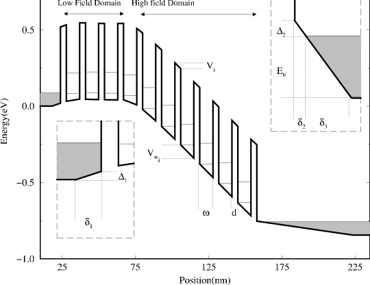
As we have discussed previously, Coulomb interaction in heterostructures with large area wells is a small effect compared with the energy difference between non-interacting eigenstates of the structure. Therefore a mean field description is, for many purposes, a good approximation. Concerning transport, the most successful modeling of these nonlinear phenomena use discrete rate equations for the electron density and electric field in each well, plus constitutive laws for the current, bias voltage, boundary and initial conditions [142, 143, 150]. The laws may be phenomenological [143] or obtained from microscopic considerations, [145, 157, 158]. In all cases cited, the boundary conditions for electrostatics were selected in a more or less ad hoc manner by using the available information from experiments. This is particularly annoying because the boundary conditions select the relevant dynamics of EFD in the oscillatory regime [159].
In order to include in a natural way boundary conditions due to the emitter and collector regions, Aguado et al [100, 122] extended the model described in Section 6.6.1 [74, 121] to consider transport in multiwell structures202020It is possible to obtain a discrete drift difussion model from the microscopic model that we present in this subsection [160]. In this discrete drift difussion model realistic transport coefficients and contact current-field characteristic curves are calculated from microscopic expressions, knowing the design parameters of the superlattice. The detailed boundary conditions obtained from the discrete model clarify the analysis of the electron dynamics and when possible self-sustained oscillations of the current are due to monopole or dipole recycling (see section 7.3 below).. The main ingredients of the sequential tunneling model are as follows: it is assumed that the characteristic time of intersubband relaxation due to scattering is much smaller than the tunneling time, which is in turn much smaller than the dielectric relaxation times responsible for reaching a steady state. This separation of time scales, as well as the configuration of a typical sample allows one to consider that: i) only the ground state of each well is populated, ii) the tunneling processes are stationary and iii) the local density in each well can be calculated from an equilibrium distribution function (Fermi-Dirac). These assumptions justify the use of rate equations for the electron densities at each well with relations for the currents calculated by means of the Transfer Hamiltonian approach [7] which gives the following expressions for the interwell tunneling currents:
| (167) | |||||
is the number of subbands in the well with energies (referred with respect to the origin of potential drops), and is the transmission coefficient through the -th barrier. The spectral function of each well is a Lorentzian, its half-width is a phenomenological parameter and roughly corresponds to the LO phonon lifetimes ( 1-10 meV) in a typical quantum well: . Of course this model can be improved by calculating microscopically the self-energies, which could include other scattering mechanisms (e.g. interface roughness, impurity effects) or even exchange-correlation effects (which affect the electron lifetime in a self-consistent way [97]). The tunneling current from the emitter to the nearest neighbor well and the current to the collector coming from its neighbor well are
| (168) |
Again, for a given set of Fermi energies the densities evolve according to the following rate equations:
| (169) |
The rate equations for the electron densities imply that the interwell currents and the currents from the emitter and to the collector are all equal to the total current in the stationary case. In these equations is the current from the emitter to the first well and the current from the -th well to the collector. denotes the set of voltage drops through the structure which are calculated from the electrostatics of the problem. Eqs. (157-158) are now generalized to describe the 2N+1 potential drops corresponding to N wells and N+1 barriers, :
| (170) | |||||
| (171) |
where is the 2D (areal) charge density at the th well (to be determined), and are the well and barrier thickness respectively. The emitter and collector layers are described by Eqs. (159) and (160).
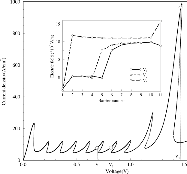
In order to close the set of equations, global charge conservation (see Eq. (161)) and applied voltage conservation (see Eq. (162)) are imposed. Instead of the rate equations (169), we can derive a form of Ampère’s law which explicitly contains the total current density . Differentiating (171) with respect to time and eliminating by using (169) one gets
| (172) |
where is the sum of displacement and tunneling currents.
The time-dependent model consists now of the equations
which contain the unknowns ,
, (), (),
, , (), , and .
This system of equations , together with appropriate initial
conditions, determine
completely and self-consistently the problem.
One way to analyse the statics of the model and the stability of
the stationary solutions is to numerically solve the
algebraic-differential system (plus appropriate initial
conditions) for each voltage until a stationary profile is reached.
This is rather costly, so a good strategy is to follow this
procedure for a given value of the bias voltage and then use a
numerical continuation method to obtain all stationary solution
branches in the current–voltage characteristic diagram. This
yields both unstable and stable solution branches. Direct
integration of the stationary equations [dropping the displacement
current in (172)] usually presents important problems of
numerical convergence to the appropriate solutions in regions of
multistability.
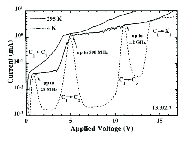
The formation of sharp discontinuities in the current–voltage characteristics (the stable branches are connected by unstable ones) can be explained by the formation of a charge accumulation layer in one of the wells (domain wall) that splits the superlattice in two regions with low and high electric field respectively. Once the ground state of the quantum well closer to the collector becomes disaligned with that of the neighbor quantum well the charge is accumulated there, producing a high electric field towards the collector and the current drops abruptly (negative differencial conductance) Increasing the voltage, this charge cannot move continuously through the superlattice. This motion can only occur for voltages allowing resonant interwell tunneling, it happens as the first excited state of the right most quantum well (the one closest to the collector) is aligned with the ground state of its neighbor well. Increasing further the voltage a new region of negative differential conductance appears and the domain wall moves from the -th well to the -th well. It produces a sawtooh like profile for the current. At large bias voltage, the high electric field region contains all the quantum wells, the field is homogeneous and the tunneling current take place from the ground state of a quantum well to the first excited level of the well located in the current direction.
An example of this system configuration is shown in Fig. 27 [122] where the current–voltage characteristics of a superlattice presenting EFD formation is plotted. The stable (unstable) branches are shown as continuous (dotted) lines. The inset shows three electric field profiles corresponding to three different voltages. They show the presence of domains in the superlattice with a domain wall which moves one well as the bias voltages changes from one branch to the next one. Domain formation is also shown in the superlattice electrostatic potential profile; see Fig. 26 for a fixed voltage V.
The first branch in the characteristics I/V Fig. 27 corresponds to tunneling ( are the conduction subbands ordered starting from that with lowest energy). As increases, tunneling becomes possible in part of the structure and domain formation does take place. The last branch (large current) appears when transport is regulated by tunneling across the whole structure. The voltage region between the peak to the peak is dubbed first plateau. At higher voltages, more plateaus can appear due to tunneling to other excited states. An interesting feature in Fig. 27 is that neighbor peaks have a smaller current than the peak. Another interesting feature due to the voltage drop at the contacts is that the number of branches in the current–voltage characteristics is less than the number of wells, in agreement with the experiments. This behavior can be understood by looking at the branch at 1.21 V where the low field domain occupies the two wells closer to the emitter. tunneling occurs between all the wells in the branch with V corresponding to an intense peak of the current, at this voltage all the quantum wells have dropped in the high field domain.
We finish this part by mentioning in passing the non-linear transport properties of weakly coupled diluted magnetic semiconductor superlattices which have been recently studied in Refs. [161, 162, 163]. The main interest of these systems is that the exchange interaction of the local moments of the magnetic impurities with the spin of the carriers, electrons or holes, produce very interesting spin-dependent properties as for instance, a very large Zeeman splitting in the presence of a small external magnetic field. The transport properties were studied for II-VI n-doped semiconductor superlattices doped with Mn. There, the interplay of the negative differential resistance regions associated with resonant tunneling, the Coulomb and the exchange interaction add a new dimension to the problem which depends crucially on the spin. Multistability of the spin polarized current and of the spin polarization of the magnetically doped quantum wells as a function of the dc voltage (i.e., multistability driven by electric fields) are an example of the interesting non-linear transport properties of these devices with potential applications in Spintronics.
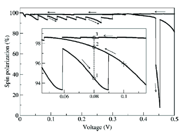
7.3 Weakly Coupled Superlattices as a paradigm of a nonlinear dynamical system II: dynamics in the undriven case
Stationary electric field domains appear in voltage biased superlattices if the doping is large enough. When the carrier density is below a critical value, self-sustained oscillations of the current may appear. They are due to the dynamics of the domain wall (which is a charge monopole accumulation layer or, briefly, a monopole) separating the electric field domains. This domain wall moves through the structure and is periodically recycled. The frequencies of the corresponding oscillation depend on the applied bias voltage and range from the kHz to the GHz regime. Self-oscillations persist even at room temperature, which makes these devices promising candidates for microwave generation [148, 149]. An experimental example from Kastrup et al in Ref. [148] is shown in Fig. 28.
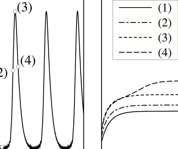
Theoretical and experimental work on these systems have gone hand
in hand. Thus the paramount role of monopole dynamics has been
demonstrated by theory and experiments. Monopole motion and
recycling can be experimentally shown by counting the spikes
–high frequency modulation– superimposed on one period of the
current self-oscillations: current spikes correspond to
well-to-well hopping of a domain wall through the superlattice. In
typical experiments the number of spikes per oscillation period is
clearly less than the number of superlattice
wells [148, 149]. It is known that monopoles are
nucleated well inside the
superlattice [148, 150] so that the number of
spikes tells over which part of the superlattice they move.
Self-sustained oscillations are not the only type of superlattice
oscillations, there are two other type that appear in the miniband
regime (in the miniband regime the quantum wells are strongly
coupled and the electronic spectrum becomes coherent minibands
extended all through the superlattice): first, oscillations occur
when the carriers within the miniband are accelerated beyond the
Brillouin zone boundary, where the drift velocity becomes
negative. In absence of scattering the electron wave packet
performs Bloch oscillations with frequency:
where and are the superlattice period and the Planck
constant respectively. These Bloch oscillations were predicted by
Esaki and Tsu[73] and many papers have followed,
inspired in the perspective of producing a superlattice Bloch
oscillator. Secondly, a different type of oscillations occur in
the miniband regime, when scattering times are shorter than the
tunneling time. In this case a transient charge accumulation
traveling through the superlattice may lead to current
oscillations.
Sánchez et al [164, 165] used the model proposed above to investigate electron dynamics in superlattices, i.e., situations where the displacement currents are non-zero and the electronic current is time-dependent. An example is shown in Fig. 30(a) [164] which depicts the current as a function of time for a dc bias voltage of 5.5 V on the second plateau of the characteristic curve of a 13.3 nm GaAs/2.7 nm AlAs superlattice consisting of 50 wells and 51 barriers, as described in [148]. Doping in the wells and in the contacts are cm-2 and cm-3 respectively.
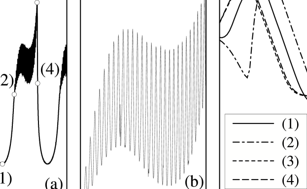
oscillates periodically at 20 MHz. Between each two peaks of , 18 additional spikes can be observed. The electric field profile is plotted in Fig. 30(b) at the four different times of one oscillation period marked in Fig. 30(a). What is remarkable in Fig. 30(a) are the spikes superimposed near the minima of the current oscillations. Such spikes have been observed experimentally and attributed to well-to-well hopping of the domain wall [149, 166]. They are a cornerstone to interpret the experimental results and in fact support the theoretical picture of monopole recycling in part (about ) of the superlattice during self-oscillations. The identification between number of spikes and of wells traversed by the monopole rests on voltage turn-on measurements supported by numerical simulations of simple models during early stages of stationary domain formation [166]. These simplified models do not predict spikes superimposed on current self-oscillations due to monopole motion [143, 148, 146]. To predict large spikes, an artificial time delay in the tunneling current [149] or random doping in the wells [167] have to be added.
When contact doping is reduced below a certain value, there appear
dipole-mediated self-oscillations, where the domain wall consists
on a charge accumulation and a charge depletion layers. There is a
range of voltages for which dipole and monopole oscillations
coexist as stable solutions. This range changes for different
plateaus. When the emitter doping is further lowered, only the
dipole self-oscillations remain. Fig. 31
[164] presents data in the crossover range (below cm-3 and above cm-3), for the same electron doping in the quantum wells
and bias voltage as in Fig. 30. Except for the presence
of spikes of the current, dipole recycling and motion in
superlattices are similar to those observed in models of the Gunn
effect in bulk GaAs [159]. These self-oscillations have
not been observed so far in experiments due to the high values of
the contact doping adopted in all the present experimental
settings. However, the contact doping is not the only parameter
which can be modified in order to have dipole oscillations in the
current. It also can be reached by modifying the sample
configuration, as for instance the quantum well widths
[160].
Bejar et al. [163] have explored interesting features
that occur in weakly doped superlattices that support
self-sustained oscillations when they are doped with magnetic
impurities. In this case, the interplay between strongly nonlinear
interwell charge transport and the large tunable spin splitting
induced by exchange interactions with spin-polarized Mn ions
produces interesting spin features. Time dependent periodic
oscillations of the spin polarized current and of the spin
polarization in both magnetic and nonmagnetic quantum wells were
predicted [163]. These spin-dependent features can
potentially be exploited for device applications, as spin
polarized current injection oscillators.
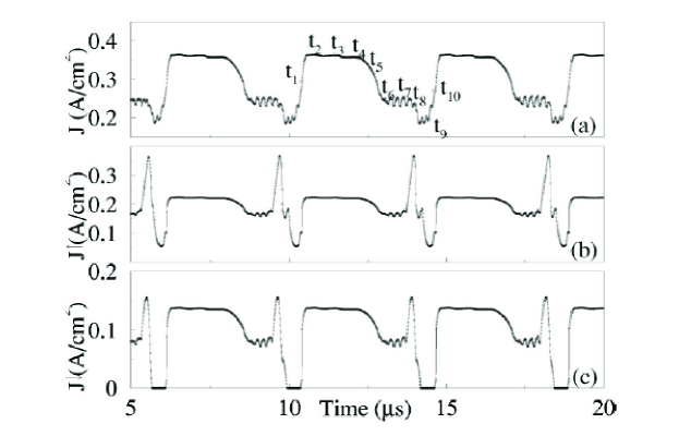
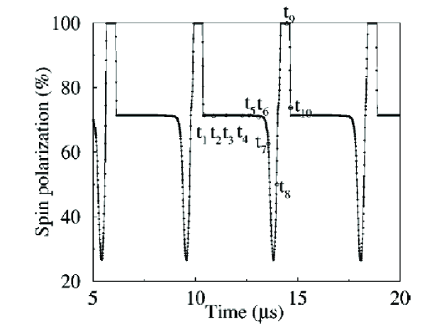
7.4 Weakly-coupled Superlattices as a paradigm of a nonlinear dynamical system III: stationary transport in the ac-driven case
The aplication of an external ac signal, superimposed to the applied dc bias voltage, drastically changes some of the nonlinear phenomena discussed above and brings about new physics not present in undriven samples 212121The calculations presented in this Section, and in Section 7.5, were performed using the selfconsistent model of Section 7.2 (only time-averaged quantities are included in the selfconsistent equations). It is thus assumed that the separation of time scales is such that it is a good approximation to neglect the selfconsistent effect of displacement currents. The modelling of nonlinear transport through superlattices in a fully dynamical and selfconsistent way constitutes an extremely dificult problem which, to our knowledge, remains open.. As an example, the current–voltage characteristics of an ac-driven superlattice displaying electric-field domain formation develop new multistability regions: Depending on the parameters of the external high-frequency field, many stable operating points, giving different dc currents, do appear at a fixed dc voltage as a result of the interplay between the strong nonlinearity and the ac-induced photoassisted tunneling channels.
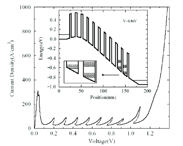
Furthermore, electric field domains supported by absorption and emission sidebands corresponding to resonant states in neighbor wells are possible: As we explained in the previous section, transport in the high (low) electric field domain is only possible by () resonances. New tunneling channels open up in the presence of an ac field thus allowing more electric field domain configurations. Experimentally, this was studied in Refs. [134, 135] (see Fig. 23).
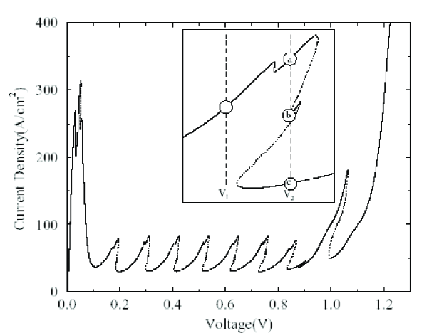
The extension of the selfconsistent method presented in subsection 7.2 to include high frequency fields was put forward in Refs. [100, 168]. The results are presented in Fig. (34) and Fig. (35). The first plot demonstrates that high field domains can be supported by photon-assisted tunneling (for this particular case tunneling involving absorption of two photons (see inset).
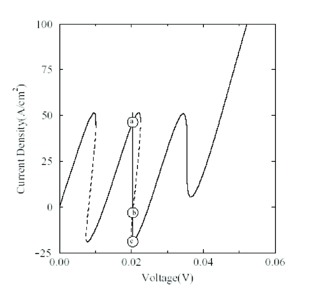
The second plot focuses on the effects of a very intense ac field when there is a high probability of having multiphotonic effects, leading to multistability of the branches. The inset shows a magnification of the first branch, the circles mark the stable operating points for a fixed voltage. At transport in the high field domain occurs via tunneling between the two-photon absorption virtual state associated with C1 and the two-photon emission virtual state associated with C2. At the branch develops a multistable solution (five solution coexist, three stable, two unstable). These solutions correspond to a different number of photons emitted in C2: one photon in the highest current stable solution (circle a), two photons in the lowest current stable solution (circle c); the process from the highest current to the lowest one involves the motion of the domain wall. The situation repeats periodically as the domain wall moves, giving the sawtooth structure in the current.
We described in Section 7.1 how it is possible to obtain absolute negative conductance in superlattices near the dynamical localization condition. In doped samples the effect can be even more spectacular for the current develops regions of bistability between positive and negative current near Dynamical Localization. This is shown in Fig. 36 [168] where the current–voltage characteristics for an irradiated sample ( and ) is plotted, for low voltages.
7.5 Weakly Coupled Superlattices as a paradigm of a nonlinear dynamical system IV: dynamics in the ac-driven case
7.5.1 High frequency driving: photon-assisted tunneling
If the carrier density of a doped superlattice is below a critical value, self-sustained oscillations of the current may appear as we have described in Section 7.3. The way an external high frequency field affects this complex dynamics has been analyzed in Ref. [169] by using the non-equilibrium Green’s function formalism described Section 5. It is straightforward to generalize the derivation of the time dependent current in Section 5, see Eqs. (60-62), and calculate the tunneling current traversing the -th quantum well from the time evolution of the particle density :
| (173) | |||||
Here, is the advanced (lesser) Green’s function which includes the effect of the ac signal and scattering processes for an isolated quantum well. The scattering processes allow a non-equilibrium quasiparticle to relax its excess energy (e.g., due to interactions with ionized impurities or LO phonons). As in the model of previous sections, a phenomenological relaxation time approximation is made by introducing a self-energy as an energy independent constant (which is denoted by ). Of course, this model might be improved by means of a microscopic calculation of due to the aforementioned scattering processes. in Eq. (173) corresponds to the retarded (lesser) Green’s function which includes tunneling events. If the same separation of time scales used in the selfconsistent model presented in subsection 7.2 holds, one can assume an equilibrium distribution function for each quantum well, since the electrons that tunnel relax their energy excess almost instantaneously. Taking into account these considerations, the effect of the ac potential consists of introducing a global phase in the expression for these Green’s functions: , where are the static retarded and lesser quantum well Green’s functions. They have the following expressions:
| (174) |
and
| (175) |
where is the Fermi-Dirac distribution function for the -th quantum well, . A similar transformation applies for . Eventually, by inserting the obtained expressions for the nonequilibrium Green’s functions [ and ] into Eq. (173), one arrives at the expression for the tunneling current between two quantum wells irradiated with a THz-field in the sequential tunneling regime:
| (176) | |||||
where is the spectral function for the -th isolated quantum well including scattering. The arguments of the Bessel functions are given by . Notice that it is assumed that the ac potential is spatially uniform along a quantum well (but different from that of its neighbors) and is independent of the quantum well index.
The current (176) may be written as
| (177) |
where is the time-averaged current. and contain higher harmonics for . In the photoassisted tunneling regime . This means that the electrons experience at least one cycle of the ac potential between two successive scattering events. In addition, the scattering lifetime represents the lowest temporal cutoff above which the assumption of local equilibrium within each quantum well holds. Therefore, the explicit time variation of vanishes and one is left with the implicit change of with respect to time. This variation (in time scales larger than ) results from the evaluation of the continuity equation for , where is the number of wells, supplemented with Poisson equations, constitutive relations, and boundary conditions, similarly to the method explained in Section 7.2, such that the current (176) is a functional of the Fermi energies and the set of voltage drops in the superlattice (denoted by ): . The total current density traversing the sample is the sum of the tunneling current plus the displacement current, i.e.,
| (178) |
where is the static permittivity, the barrier width, and the voltage drop in the th barrier.
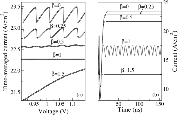
Solving selfconsistently at each time step the above set of
equations López et al [169] demonstrate that the
photon field with frequency in the range of THz is able to
induce low-frequency self-sustained current oscillations in
superlattices with frequencies in the range of MHz as
in the undriven case.
This is shown in Fig. 37a, where the time
average of is plotted as a function of the
applied dc bias voltage, . Without ac, the –
curve shows branches after the first peak. As we have discussed in
Section 7.2 this is characteristic of
static electric field domain formation. In the presence of an ac
signal, the branches become smoother (), and finally
they coalesce and a plateau clearly forms (). This is the
key signature of current self-oscillations. We described in
Section 7.2 how the electric field domain
configuration becomes unstable with decreasing the doping density
such that self-sustained current oscillations occur due to the
periodic recycling of the domain wall. Here the same effect is
induced by the ac signal. By increasing further, the
plateau starts to be replaced by a positive differential
resistance region. There is a similar well-known phenomenon in
weakly coupled superlattices driven only by dc voltages: under a
critical value of the carrier density neither static nor moving
domain walls exist and the electric field drops homogeneously
across the whole sample. The transition from static to
time-dependent current maybe also effectively achieved at constant
carrier doping by either applying a transverse magnetic field
[170] or raising the temperature [171].
Here, the doping density is constant and it is the ac potential
that tunes this transition. This is illustrated in
Fig. 37b where for a fixed
bias voltage is plotted. For , the current
achieves a constant value after a transient time. As
increases (), the current oscillates with a frequency in
the range of MHz, much smaller than . This is a result
of the motion of the accumulating layer of electrons, and its
recycling in the highly-doped contacts (see below). Then the ac
potential induces a transition from a stationary configuration
toward a dynamic state likely via a supercritical Hopf
bifurcation. Below, it is shown that the existence of
photosidebands and their influence on the non-linear behavior of
the system drives the superlattice toward oscillations. For
the current is damped and reaches a
uniform value. This is a striking feature— an oscillation
disappearance induced by an ac potential.
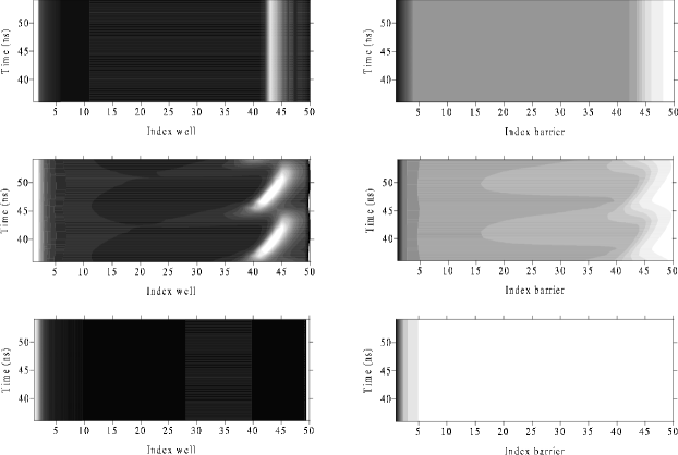
The ac induced transition from static electric field domains
toward homogeneous field distributions through self-sustained
current oscillations is illustrated in
Fig. 38. We observe how the charge density
through the structure, at fixed dc bias voltage, undergoes a transition
from being accumulated in the 43th quantum well, independently of
time (stationary electric field domains) at zero ac potential, to
presenting periodic oscillations (=1). Increasing
further (=1.5) a homogeneous charge distribution is reached
and the electric field and charge are uniformly distributed
through the sample (with small inhomogeneities at the emitter
contact). A qualitative explanation of this transition is as
follows:
Let denote the average drift velocity due to tunneling
between two QW’s with local electric field . Within a
semiclassical approximation, the current (176) can be
approximated by , where the
electronic drift velocity is given by . Here, the current is evaluated by using
Eq. (176) after imposing and setting an
average interwell electric field along the superlattice period
[160]. The contribution from
diffusivity, which can be important at very low electric fields
[160], is neglected. As shown in
Ref. [172], the sufficient condition for stationary
electric field domains to form reads:
| (179) |
where () is the maximum (minimum) electron drift velocity attained at an electric field given by (). Unlike the minimum velocity, the maximum drift velocity is very sensitive to the external ac potential. We see from the time average of Eq. (176) that first current peak (i.e., ) is weighted by at low values of (the zero-photon peak). As increases, the THz potential produces photoassisted tunneling with absorption and emission of photons. As a result, the zero-photon peak is quenched as the contribution of terms with begins to grow. As we have seen in previous Sections, this is a consequence of the photoassisted formation of sidebands. The overall effect is that decreases as increases. For a certain critical value of [; see Fig. 37(b)], one finds and the steady electric field domain configuration is no longer stable. The system evolves spontaneously toward self-sustained current oscillations. On the other hand, once the dynamical configuration is stable, increasing will tend to drive the superlattice to a trivially homogenous electric field profile (see Fig. 38, lower panel). The reason for that is the complicated shape of the time-averaged drift velocity induced by the ac potential. The ac potential opens up new tunneling channels due to photon absorption and emission and their relative weight and their contribution to depend in a non trivial way on the ac frequency and intensity, the sample characteristics and the scattering processes involved. This can lead to a – curve exhibiting positive differential resistance with a Z shape unlike the electric field domain case, which exhibits a – curve with a N shape [172] Of course, this qualitative argument does not provide with an estimate of the different transition points but still shows conclusively that an ac field may induce a dynamical transition from stable stationary domains to traveling field domains and a homogeneous electrostatic configuration by modifying the effective electronic drift velocity with the dimensionless ac parameter .
Finally, we finish this part by mentioning a recent work by Batista et al [173] where the intersubband transitions in n--doped quantum wells strongly driven by far infrarred radiation is studied. They demonstrate that a suitably taylored quantum well can exhibit superharmonic generation and nonlinear phenomena in their absorption lineshapes. In their study they show that intersubband transitions can produce strong subharmonic (period doubling) or a strong inconmensurate (Hopf) frequency response by varying the density and the intensity.
7.5.2 Adiabatic driving: routes to chaos
The rich dynamical behavior an ac signal induces in a superlattice is not restricted to the high frequency regime. Driving a superlattice with a low-frequency signal, in particular for frequencies of the ac field inconmensurated with the natural frequency of the system, produces quasiperiodicity, frequency locking or chaotic current as a function of the intensity of the driving field. Intriguing routes to chaos, reflected in complex bifurcation diagramms, have been experimentally observed in semiconductor superlattices driven by an ac field.
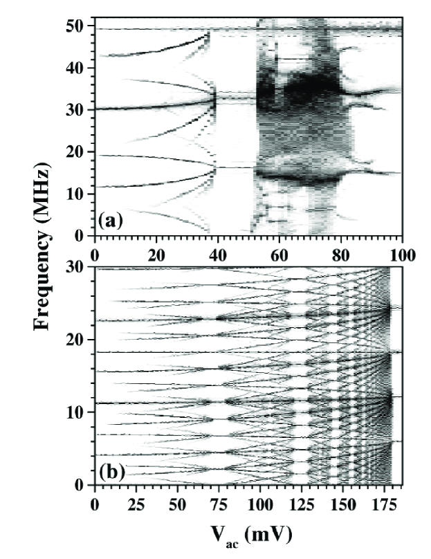
[152, 153, 154, 155, 174]. Many studies fix the frequency of the ac drive as the golden mean number times the frequency of the natural oscillations (i.e., the frequency ratio is an irrational number hard to approximate by rational numbers), which is convenient to obtain complex dynamical behavior. In this case, the system presents a rich power spectrum, a complex bifurcation diagram and different routes to chaos including quasiperiodicity, frequency locking, etc. [152, 153, 154, 155, 174].
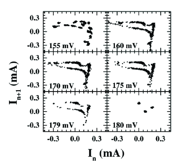
First return or Poincaré maps are used to analyze unambiguously the underlying attractors [155]. In the quasiperiodic case, Poincaré maps usually consist of smooth loops, whereas they are a set of discrete points in the case of frequency locking. More exotic Poincaré maps resembling distorted double loops in the quasiperiodic case have been experimentally observed in middle of the second plateau of the current–voltage characteristic of a superlattice [154, 155]. At the onset of this plateau, Poincaré maps are smooth and not distorted. The origin of distorted maps was not understood at the time of their observation, although disorder and sample imperfections were invoked [154]. Luo et al [155] showed that a combination of signals with different frequency was needed in order to reproduce experimentally observed distorted double layer Poincaré maps. The origin of this combination was not ascertained in that work. By using the model of section 7.2, Sánchez et al have shown in Ref. [175] that high-frequency current spikes of the self-oscillations give rise to these exotic Poincaré maps. In turn, current spikes are due to the well-to-well motion of the domain wall during each period of the self-oscillations. Thus distorted Poincaré maps reflect the domain wall motion in ac driven superlattices. They analyze the sequential tunneling current with an applied voltage, , where where is set to the golden mean times the natural frequency of the system.

Namely, is very small compared with typical energy scales of the system such that modifies adiabatically the potential profile of the superlattice. Thus, the condition that all voltage drops across the different regions of the nanostructure must add up to the applied bias voltage, c.f. Eq. (162), is in this case:
| (180) |
where and are the potential drops in the
i-barrier and well respectively and and
correspond to the potential drops at the contacts,
c.f. Eqs. (157–160).
The results are shown in Fig. 41 where the evolution of
the current through the superlattice, its Fourier spectrum and its
Poincaré map for V and mV are plotted.
These values correspond to the onset of the second plateau of the
– characteristic curve. For the doping values taken (see
caption) self-oscillations are due to recycling of monopole domain
walls.
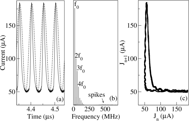
The current trace of Fig. 41(a) is quasiperiodic and does not present observable superimposed high-frequency oscillations (spikes). The natural oscillation near the onset of the plateau is caused by monopole recycling very close to the collector contact. Thus the DW does not move over many wells and the current trace does not present an appreciable number of spikes. In the power spectrum of Fig. 41(b) there are contributions coming from the fundamental frequency MHz, the frequency of the applied ac field , the combination of both and their higher harmonics. The Poincaré map depicted in Fig. 41(c) is a smooth loop with a nontrivial double layer structure indicating quasiperiodic oscillations. By reducing the doping of the contacts, (solid line in Fig. 42(a)) deviates from a sine (dotted line Fig. 42(a)) due to the presence of spikes at low currents values which results in higher harmonics in the frequency spectrum (Fig. 42(b)). The first return map gets a strong distortion (see Fig. 42(c)) such that it can be concluded that the presence of spikes give rise to the wiggles that ultimately cause the twist of the loop (note that the twisted arm ranges from about 49 A to 55 A, exactly the region covered by the spikes in Fig. 42(a)).

The previous conclusion may be reinforced by changing the dc voltage to =1.5 V (middle of the first plateau) such that the frequency of the natural oscillation is now reduced to 4 MHz, presents dipole-like oscillations and superimposed finite amplitude spikes (Fig. 43(a)). The Poincaré map, Fig. 43(c), is much more complicated than in the previous case, showing three well defined distorted loops. Since loops in the Poincaré map are due to combination of strong enough signals of different frequencies [155], the greater strength of the high-frequency spikes gives rise to the additional loop structure and higher harmonic content (Fig. 43(b)). Therefore, the high frequency selfsustained oscillations or spikes are essential to explain the observed electronic trajectories and the complicated electronic dynamics in a low frequency ac-driven multiquantum well structure [175].
Finally, we finish this part by mentioning that a detailed analysis of the routes to chaos in low frequency ac-driven weakly coupled superlattices with magnetic impurities has been recently performed [176].
7.6 Strongly Coupled Superlattices in ac potentials
In a pioneering paper, Esaki and Tsu proposed high frequency oscillators by tayloring the non linear electronic transport properties of semiconductor superlattices [177]. Strongly coupled superlattices are characterized by energy bands, the so-called minibands, instead of discrete levels. The corresponding extended states are Bloch states. In the presence of a constant electric field , the Bloch states are no longer eigenstates of the Hamiltonian: the electrons are accelerated by the electric field and perform a repetitive motion of acceleration and Bragg reflexion called Bloch oscillation, characterized by the Bloch frequency: where is the superlattice period222222For a review on transport in superlattices see Ref. [178]..
The effect of radiation on the transport properties of superlattices in the miniband regime has been experimentally analyzed by different groups during the last two decades. These experiments demonstrate that the application of an external ac field to a superlattice in the miniband regime induces a great deal of interesting phenomena.
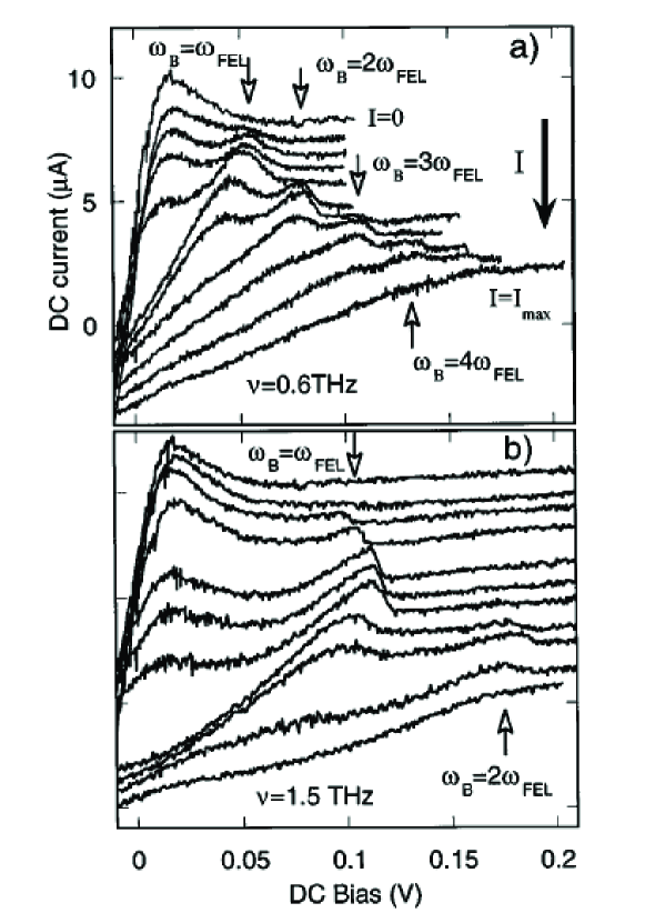
As we described in subsection 3.3 an external ac field can produce the collapse of the miniband width at the dynamical localization condition as demonstrated by Holthaus in Ref. [29]. A similar effect was observed by Ignatov and coworkers [32, 33] who reported ac-field-induced reduction of the dc current. They attributed such a reduction to a frequency modulation of the Bloch oscillations of electrons at the frequency of the external ac field. The group of Santa Barbara [179] observed what they called the inverse Bloch oscillator effect, which consists of resonant changes in the current-voltage characteristics when the Bloch frequency is resonant with a THz field and its harmonics. An example from these experiments is shown in Fig. 44.
The nonlinear dynamics of miniband superlattices under irradiation have been analyzed by Alekseev and coworkers in a series of papers [180, 181, 182]. Interestingly, they show in Ref. [182] that a purely ac external field applied to an unbiased superlattice can create a dc bias voltage and thus spontaneously generate a dc current. In technical terms, this can be explained as a spontaneous breaking of spatial symmetry induced by the external field.
Finally, we mention another interesting effect induced by dynamical localization: Meier et al [183] analyzed how and external ac field can alter the effective dimensionality of the excitons in a superlattice. Based on a full three dimensional description of both coherent and incoherent phenomena in anisotropic structures, they found that appropiated applied oscillating fields change the exciton wave function from anisotropic three dimensional to basically two dimensional. This effective dimension change is caused by dynamical localization which leads to an increase of the exciton binding energy and of the corresponding oscillator strength.
8 Microwave-induced zero resistance in two-dimensional electron gases
Recently, the study of two-dimensional electron gases irradiated by microwaves has received a great deal of attention due to the observation of microwave-induced zero longitudinal resistance in two-dimensional electron systems at low magnetic fields (just below the onset of Shubnikov-de Haas oscillations) [184, 185]. In the presence of microwaves, the longitudinal resistance oscillates (with minima reaching zero-resistance and even negative values) as a function of the inverse of the applied magnetic field with a period given by , where is the microwave frequency and the effective electron mass, see Fig. 45. An explanation for this intriguing phenomenon was given by Durst et al in Ref. [186]. Similar arguments were presented by Anderson and Brinkman in Ref. [187] and by Shi and Xie in Ref. [188]: If an electron absorbs a microwave photon , where is the cyclotron energy which defines the spacing of the Landau-level ladder (which is tilted by the applied dc voltage), no transport is possible. If, on the other hand, , energy can be conserved if impurities scatter the electron laterally. The upstream or downstream motion will reduce or increase the conductivity of the sample. If the final density of states to the left exceeds that to the right the current is enhanced. If vice versa, the current is diminished such that the scattering events can drive the conductivity to zero or even negative values if the electrons tend to flow uphill.
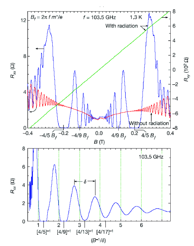
The above physical picture can be understood by the following simple model [188]: Let us consider a junction biased by an ac voltage and assume that the left and right regions have the same density of states such that the current and the conductance can be written as (see Section 2):
| (181) | |||||
The second term in the expression for the conductance depends on the derivative of the density of states, and can be either positive or negative. The contribution from the second term is purely due to the photon-assisted tunneling process, and vanishes when there is no ac field. If one now assumes a density of states which is a periodic function of energy near the Fermi surface, with period , the simple toy model in Eq. (181) captures most of the important features of the experiments [184, 185]. In particular, if one takes
| (182) |
where is a dimensionless constant representing the fluctuation amplitude of the density of states, a straightforward calculation yields the conductance of the system,
| (183) | |||||
where , and is the contribution from the Shubnikov-de Hass oscillation which diminishes rapidly at finite temperatures. The conductance oscillation minima can be easily determined from Eq. 183: for the th harmonics of the oscillation, the positions of the conductance minima are given by the equation , where . For , it yields the conductance minimum positions very close to , although not exactly. When the higher orders of harmonics become important, one can expect that the conductance minima deviate from the rule. The amplitude of oscillation is independent on the temperature, namely any temperature dependence observed in the experiments should come from the temperature dependence of the density of states, i.e., . By using a more realistic density of states taking into account that in a 2DEG under a perpendicular weak magnetic field is a function of
| (184) |
where is the relaxation time of electron which depends on the scattering mechanisms of the system and the temperature, the agreement with the experimental observation is quite good: The conductance minima are found at the positions near for the low and intermediate intensities of the microwaves. As in the experiments [184, 185], one gets two sets of crossing points at and , where the conductances equal their dark field values.
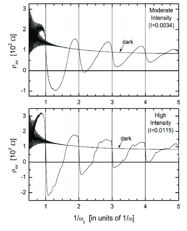
Note that we have discussed here the behavior of the conductance whereas the experiments measure resistance. The connection can be made by rebembering that in a Hall bar the relation between conductance and resistance is:
| (185) |
As pointed out by the authors of Ref. [186], the experiments are in the regime where and such that and have the same microwave-induced period and phase ( remains unafected by the external radiation).
The simple picture given by Eqs. (181-184) is confirmed by a more ellaborated calculation by Durst et al [186] who evaluate the conductante using a diagramatic selfconsistent Born approximation including radiation and disorder. An example of their calculation in shown in Fig. 46 where vs at fixed and different values of the radiation intensity is plotted. In agreement with the experiment, the period of the oscillations is and minima are found near . The authors note that the 1/4 phase shift is not universal, varying between 0 and 1/2 depending upon disorder and intensity.
Andreev et al [189] noted that a negative conductivity makes the two-dimensional electron gas unstable. Due to this instability the systems develops a domain structure with an inhomogeneous current pattern, for which the measured resistance would be zero. Other explanations have also been proposed in the literature [190, 191, 192].
Finally we mention that the phenomenon of ac-induced negative conductance in two-dimensional electron gases bears close resemblance with the ac-induced negative resistance observed in THz-irradiated superlattices we have discussed in subsection 7.1.
9 Electron pumps
We have seen in previous sections that the application of an ac signal to a semiconductor heterostructure brings about a good deal of new phenomena like, for instance, coherent destruction of tunneling or absolute negative conductance in semiconductor samples which are biased with a positive voltage. This latter phenomenon is just an example of a general class of systems dubbed electron pumps where current rectification is achieved by combining nonlinear ac driving with either absence of inversion symmetry in the device, or lack of time-reversal symmetry in the ac signal. The range of possible electron pumps includes turnstiles [193, 194], photon-assisted pumps [195, 196, 197, 198, 199] or adiabatic pumps [200, 201, 202, 203, 204, 205, 206, 207, 208, 209, 210, 211, 212, 213, 214, 215, 216, 217, 218, 219]. Ratchets are another example of systems where the combined action of nonlinearity, noise and asymmetry also produces current rectification [220, 221, 222]. Here we focus on coherent quantum pumping.
In general, coherent quantum pumping appears when traversal paths of different energy interfere in the presence of an oscillating scatterer. A complete description of quantum pumps, both adiabatic and nonadiabatic, in terms of Floquet scattering theory [37, 38, 45, 223, 224] has been put forward by Moskalets and Büttiker in Ref. [219]. As we have described in subsection 4.2, the Floquet scattering theory deals with the scattering matrix dependent on two energies (incident and outgoing). The matrix element , with , is the quantum mechanical amplitude for an electron with energy entering the scatterer through lead to leave the scatterer through lead having absorbed () or emitted () energy quanta. , , number the leads connecting the sample to reservoirs. Thus, all the quantities of interest are expressed in terms of the side bands [43] corresponding to particles which have gained or lost one or several modulation quanta .
In particular, by expressing the annihilation operator for outgoing particles in the lead in terms of annihilation operators for incoming particles in leads , 232323 means a sum over those (positive and negative) for which (the negative values correspond to bound states near the oscillating scatterer which do not directly contribute to the current) [219]., the distribution function for electrons leaving the scatterer through the lead , , can be related with the distribution function for electrons entering the scatterer through lead , , as:
| (186) |
Using Eq. (186), the current directed from the scatterer towards the reservoir
| (187) |
can be rewritten as:
| (188) |
By using current conservation, , Eq. (188) can be expressed in a very useful representation:
| (189) | |||||
In a typical pump setup, incoming electrons in all the channels can be described by the same Fermi distribution function (the electrochemical potential of the incoming electrons is the same throughout the whole structure) such that the pumped current is:
| (190) |
The existence of the pump effect is thus directly related to the symmetry of the scattering problem. By considering all possible symmetries, Moskalets and Buttiker conclude that in the adiabatic case () only a scatterer without spatial and time reversal symmetry can produce a directed current. On the other hand in the nonadiabatic case (at large pumping frequency) to achieve pumping it is necessary to have a scatterer with either broken spatial or time reversal symmetry.
As an example, let us now consider the effect of time reversal symmetry (TRS) on the pumped current 242424the time reversal interchanges incoming and outgoing channels .: in the presence of TRS, Eq. (190) reads:
| (191) |
If the pump generates a current. Based on this principle, Wagner and Sols proposed in Ref. [197] a pump in which the current is carried deep within the Fermi sea. An schematic potential profile of this pumping device is shown in Fig. 47.
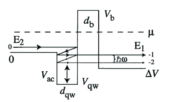
In this device, a quantum well is driven harmonically by an external ac potential . Adjacent to the well is a static barrier, and the overall potential profile features a band offset between the left and right leads. The chemical potential is the same throughout the whole structure such that any dc current flowing is thus due to the combined effect of the driving ac force and the spatial asymmetry of the model. The current can thus be written as:
| (192) | |||||
| (193) |
where is the density of states in the dimensions perpendicular to the direction of transport and where
| (194) |
The pumped current in Eq. (192) can be numerically obtained by employing the transfer-matrix technique [197, 198]. Interestingly, it is shown that the pumped current is carried by electrons which, for sufficiently high Fermi energies, may stay well below the Fermi surface, thereby rendering the total current insensitive to temperature. This remarkable effect can be explained in terms of the pipelines displayed by the total transmission probability of the device. Pipelines are pairs of left and right scattering channels, of energies , that are strongly coupled.
Indeed, the minimal model, that consisting of a single pipeline [197, 198], reproduces analytically the main features obtained from the full numerical calculation of the transfer matrix equations. Let us consider a single pipeline of strength connecting the energies on the right and to the left. Assuming incident electrons approaching the device outside these two channels to be reflected with unit probability, the transmission probabilities read:
| (195) | |||||
| (196) |
such that
| (197) |
In the single-pipeline model, the pumped current in Eq. (192) reads:
| (198) |
For one spatial dimension, Eq. (198) translates into
| (199) |
which has a peak at = , and an exponential decay for . In 2D,
| (200) |
where Li is the polylogarithm function. Expanding for , one finds that in 2D the pump current decays only algebraically as . Finally, in 3D
| (201) |
For one has 1 and 0, i.e., the current in 3D becomes independent of in this limit, = . It is interesting to analyze the spectral function (193) that leads to the pump current. Within the single–pipeline model, one obtains
| (202) |
In the particular case of three dimensions, and Eq. (202) yields a square function localized between and . The total current is a convolution of with a thermal population of incoming electrons, see Eq. (192), such that for the pump current is sustained by scattering states with incident energy well below the Fermi surface. As a consequence the current in this regime is insensitive to temperature, even for .
10 Photon assisted tunneling in quantum dots I: Coulomb blockade regime
In this part we discuss electron transport on semiconductor quantum dots that are driven by microwaves. In particular, we shall focus on lateral quantum dots 252525Other configurations, also termed quantum dots in the literature, include nanocristals, self-assembled quantum dots and vertical quantum dots. For a review, see Refs. [225, 226].. The starting point for these devices is a two-dimensional electron gas (2DEG) at the interface of a semiconductor heterostructure (typically GaAs/AlGaAs). To define the quantum dot, metallic gates are patterned on the surface of the wafer by means of electron-beam lithography. Negative voltages applied to the metallic surface gates deplete the 2DEG underneath, defining a small confined region (the quantum dot) with a typical size of . The resulting dot contains a few electrons and is coupled to the large 2DEG regions (electron reservoirs) by tunnel barriers. These kind of systems are very suitable for quantum transport studies because of their tunability (level spacing, charging energy, barriers, etc). One can estimate the charging energy (energy needed to add an extra electron to the system, see below) and the level spacing from the dimensions of the dot. Typical values are and . Although the typical number of electrons in lateral quantum dots is of the order of hundred, the experimental challenge of realizing few-electrons quantum dots in lateral geometries has been recently achieved by the groups of Ottawa [227] and Delft [228].
Transport through a quantum dot occurs when the Fermi energy of the leads is aligned with one of the discrete energy levels of the confined region. This resonant current, due to elastic tunneling of electrons between the leads and the dot, is strongly modified in the presence of microwaves: when an additional time-dependent potential is applied to the central gate, the electrons can exchange photons of energy with the external field with typical experimental frequencies which range from 1-75GHz. These inelastic tunneling processes, namely photon assisted tunneling, lead to drastic changes in the dc transport through these devices [229, 230, 231, 232, 233].
At zero temperature (and neglecting cotunneling) transport occurs if the electrochemical potential of the quantum dot lies between the electrochemical potentials of the reservoirs and , where is the applied bias voltage .
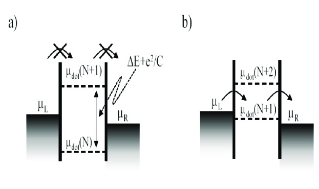
The electrochemical potential of the dot is, by definition, the minimum energy needed to add the Nth electron to the dot: , where is the total ground state energy for N electrons on the dot at zero temperature. Apart from the quantization of the energy levels, the confinement leads to charge quantization if , where is the tunnel resistance of the barriers and is the resistance quantum. This charge quantization makes it essential to take into account Coulomb interactions when calculating the ground state energy of a quantum dot.
The simplest model taking into account charge quantization for describing transport is the Coulomb blockade model. This model parametrizes the Coulomb interaction by means of a capacitance , i.e the sum of the capacitances of the barriers and the capacitance of between the dot and the gate, such that
| (203) |
is the total energy of N independent electrons. When at fixed gate voltage the number of electrons changes by one, the change in electrochemical potential is:
| (204) |
The addition energy consists of two terms: a purely electrostatic part , which is large for a small capacitance, and the energy spacing between two discrete quantum levels. Note that if two electrons are added to the same spin degenerate level . At low temperatures, , the charging energy dominates transport. When the electron transport is blocked, namely the quantum dot is in the Coulomb Blockade regime (see Fig. 48a).
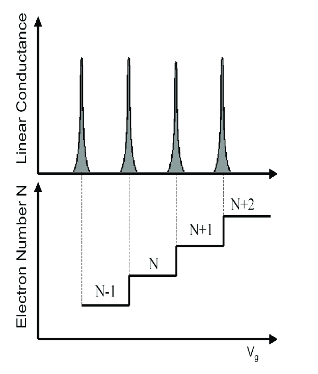
The Coulomb blockade can be removed by changing the gate voltage, to align between the chemical potentials of the reservoirs (Fig. 48b) such that an electron can tunnel from the left reservoir to the dot and from the dot to the right reservoir, which causes the electrochemical potential to drop back to . A new electron can enter now the dot such that the cycle is repeated. This process is called single electron tunneling. By changing the gate voltage, the linear conductance oscillates between zero (Coulomb blockade) and non-zero. In the regions of zero conductance, the number of electrons inside the quantum dot is fixed (see Fig. 49).
Assuming sequential tunneling of single electrons, the current can be calculated with a master equation approach [234] or by means of nonequilibrium Green s function techniques [62] (see section 5). Here, we describe the master equation approach which is probably the simplest method that allows for a qualitative explanation of the Coulomb oscillations of the conductance. The master equation method generalizes the ”orthodox theory” [236] for SET in metal systems to include 0D-states.
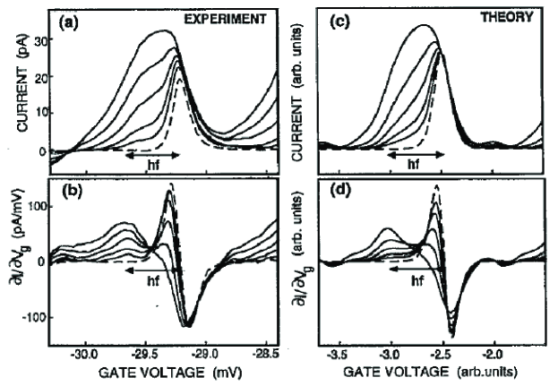
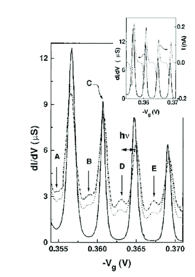
The Coulomb oscillations are modified by the application of microwaves to the gate voltage. This effect can be included in a master equation that takes into account Coulomb blockade and photon-assisted tunneling by writing the tunnel rate through each barrier in the presence of microwaves in terms of the rates without microwaves in the Tien and Gordon spirit [237, 238, 239]:
| (205) |
The modified rate , reflects the appearance of new channels for transport, the so-called photon sidebands, which correspond to emission and absorption processes.
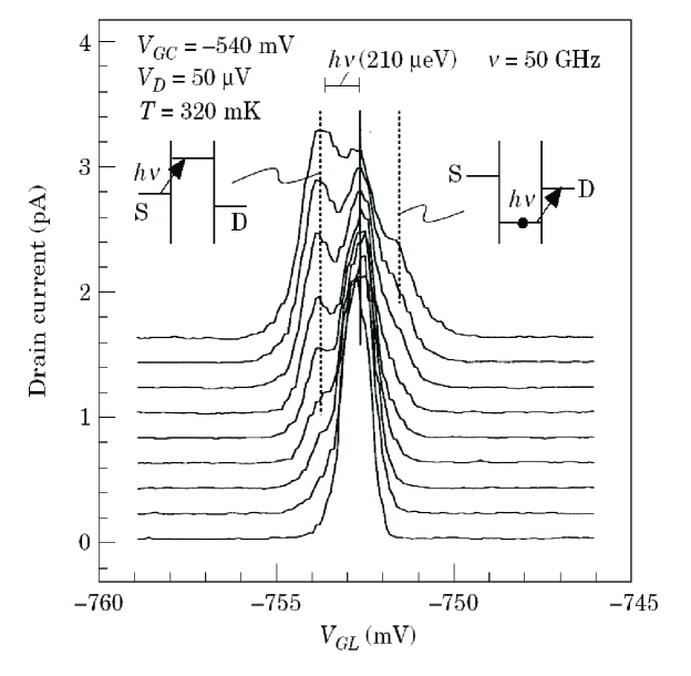
In the master equation, one has to keep track of the particular occupation of the electrons in the single particle levels for a given number of electrons . If the electrons are distributed over levels, the number of different configurations is given by a binomial factor . Assuming , only two charge states, have to be taken into account such that the probability for state is calculated from the set of master equations:
| (206) | |||||
and a similar equation for . In the stationary limit , which together with the boundary condition , close the set of equations to be solved.
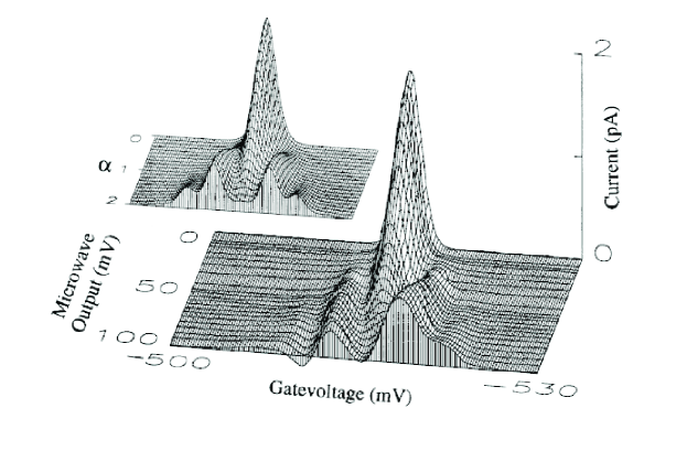
The first term of Eq. (206) describes tunneling out of states that leave the dot in . The second term describes tunneling onto the dot and all the empty states have to be taken into account. These processes are described by the rates:
| (207) |
where are the tunneling rates through the left and right barrier evaluated at energy , are the Fermi functions of the reservoirs and the coefficients describe the asymmetry of the dc voltage drop across each barrier.
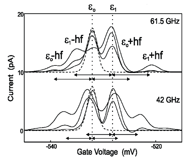
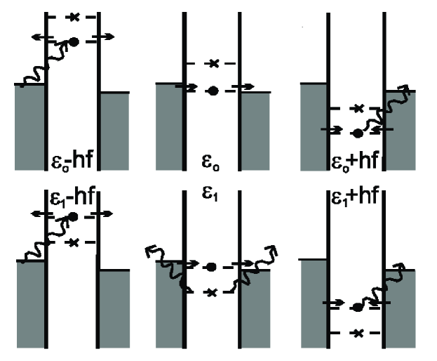
The last two terms of Eq. (206) describe relaxation and excitation processes where the number of electrons inside the dot remains fixed. The dc current can be calculated, for instance, from the net tunneling rate through the left barrier:
| (208) |
We mention in passing that Eq. (205) is a particular example of a general description of the effects of an external fluctuating environment on single-electron tunneling. In general,
| (209) |
where is the espectral density characterizing the environment. Eq. (209) describes a modified rate in the presence of an environment with fluctuations which are broad band in frequency: finite impedance of the leads [240], phonons [241], quantum noise [242], etc. Eq. (205) is thus a particular example describing a monochromatic environment.
Many of the experiments on photon-assisted tunneling in quantum dots can be explained in terms of the Tien-Gordon theory. An example is shown in Fig. 50 where we plot a comparison between experimental and theoretical data by Kouwenhoven et al [230]. In this experiment, the Coulomb blockade peaks develop shoulder structures in the presence of the microwave signal. Later, Sun and Lin anayzed in detail these experiments [243] by using the nonequilibrium Green’s functions technique (see section 5). They concluded that the shoulder structure can be explained if one assumes a strong asymmetry of the applied ac signal (their results are in good agreement with the experiments of Ref. [230] when the ac potential is applied only to one lead). Similar experiments at higher frequencies were performed by Blick et al in Ref. [231] (see Fig. 51). The position of the shoulder in the photon-assisted tunneling curves of Fig. 50 is independent of power and shifts linearly with frequency, which unambigously indicates photon-assisted tunneling. In this experiment the effective density of states of the dot is continuous and there is no evidence of the 0D-states.
Later experiments [232, 233, 244] demonstrated that it is possible to perform transport spectroscopy through 0D states by studying photon-assisted tunneling on smaller dots. If , microwave frequencies smaller than the average level spacing, the transport occurs through only a single level. In this case, at both sides of the main peak, sidebands do develop at multiples of corresponding to the emission and absorption of photons. An example from the experiment by Fujisawa and Tarucha [232] is shown in Fig. 52 where the sidebands due to photon-assisted tunneling can be clearly resolved as one increases the microwave power at fixed frequency. The amplitude of the nth sideband, namely the probability of absorption and emission of the nth photon, is given by , i.e. the probability changes nonlinearly when the microwave power is increased, as predicted by the rates of Eq.(205). A systematic study of this power dependence was performed by Oosterkamp et al [244]. We show in Fig. 53 one of their experimental curves where the current as a function of the gate voltage, for different microwave powers and fixed frequency (, and ), is plotted. For comparison, a calculation of the current using Eq. (206) (and assuming equal ac voltages across each barrier) is also shown. The agreement between experiment and theory is very good, the small difference bewteen both curves can be explained by taking into account the asymmetry in the ac voltage drop across each barrier.
When , photon-assisted tunneling can induce current through excited states such that new peaks at gate voltages given by do appear. These kind of experiments have been performed by Oosterkamp et al [233] where they show that photon assisted tunneling can lead to transport through excited states in a process similar to the photo-ionization of atoms. In the presence of microwaves a new resonance appears on the right side of the main resonance (Fig. 54). This can be explained as photo ionization of the quantum dot followed by tunneling through the first excited state as illustrated in Fig. 55. These experiments were analyzed theoretically in Refs. [245, 246].
11 Photon assisted tunneling in double quantum dots
In the previous section we have described how photon-assisted tunneling can be used as a powerful spectroscopic tool to extract information about internal energy scales of a quantum dot. The natural extension of this idea, namely performing photon-assisted tunneling in systems consisting of two or more coupled dots has proven to be extremely fruitful during the last years. By coupling two quantum dots in series one defines a double quantum dot, which can be regarded as an ’artificial molecule’.
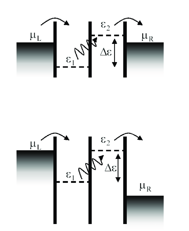
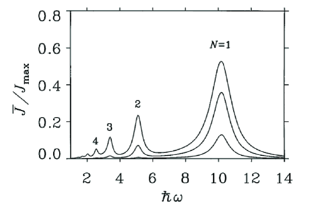
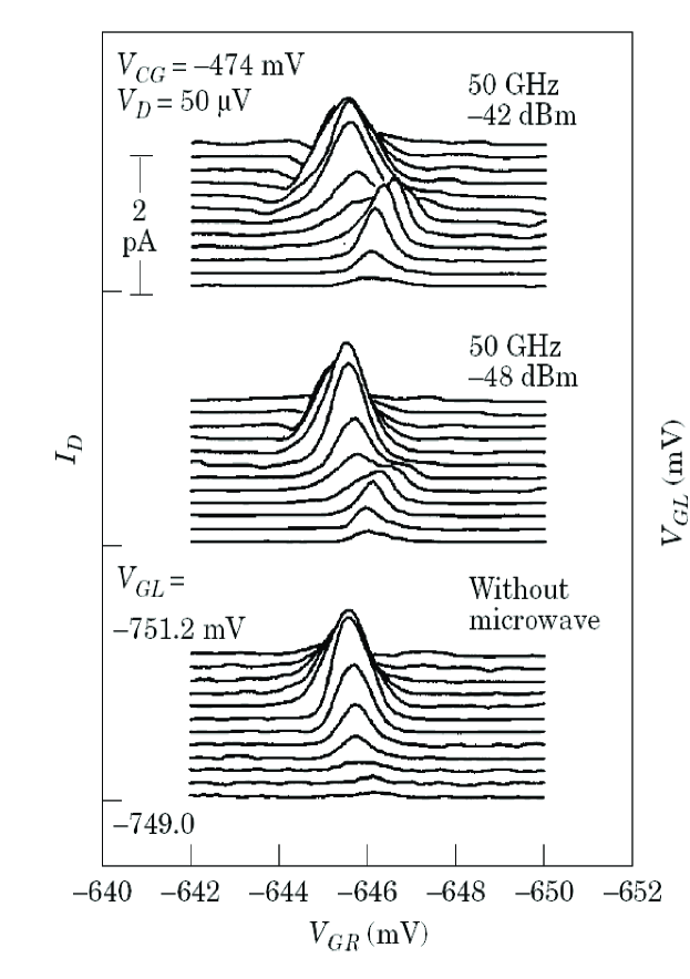
Depending on how strong is the inter-dot tunneling coupling (which can be tuned by a gate voltage), the two dots can form ionic-like molecules (weak inter-dot tunneling coupling) or covalent-like molecules (strong inter-dot tunneling coupling). If the double quantum dot is tuned such that only the topmost occupied level on each dot is taken into account, this device is an artificial realization of a quantum two level system. This description of the double quantum dot as an effective two level system is correct as long as transport occurs due to resonant tunneling between the ground states of both dots: namely, starting from the ground state with N electrons in the left dot and M electrons in the right dot, the transport occurs between the states and 262626A detailed description of transport in double quantum dots can be found in the review of Van der Wiel et al in Ref. [247]..
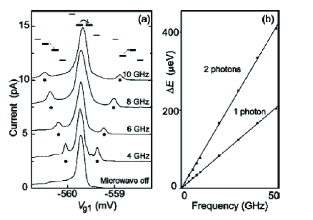
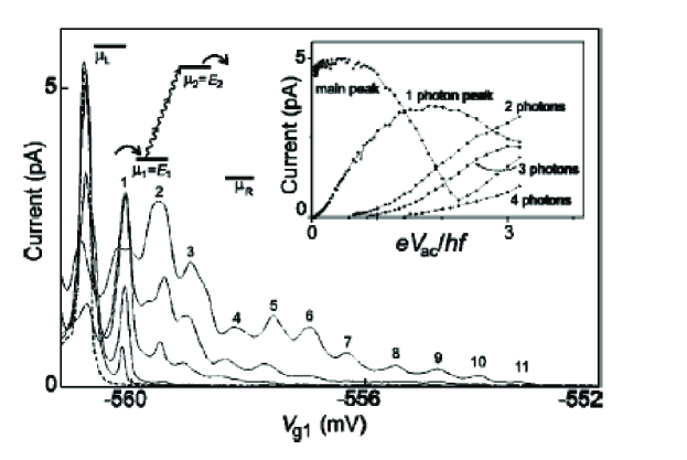
The basic idea when performing photon-assisted tunneling spectroscopy is to measure the energy differences between states in the two dots by using microwaves (typical frequencies ranging from 0-75GHz) [232, 248, 249, 250, 251]. Without microwaves, a resonant current flows through the double quantum dot device provided that , where and and are the chemical potentials and the discrete energy levels of the quantum dots respectively. In the presence of microwaves,the conditions for transport change because the external field can induce inelastic events such that . Experimentally, this idea was first put forward by Blick et al in Ref. [251] and by Fujisawa and Tarucha in Ref. [232].
To use photon-assisted tunneling as a spectroscopic tool for double quantum dots, two different configurations can be used: pumping [196, 252] and large bias voltage [253]. The pumping configuration is operated at zero bias voltage across the system, absorption of a photon with energy leads to a finite dc current which is positive or negative depending on the sign of (Fig. 56, upper graph). photon-assisted tunneling spectroscopy in double dots can also be investigated in the large bias voltage case, where both absorption and emission contribute to a positive dc current (Fig. 56,lower graph).
11.1 Photon-assisted tunneling in weakly coupled double quantum dots I: pumping configuration.
Photon-assisted tunneling in weakly coupled double quantum dots in the pumping configuration was first investigated theoretically by Stafford and Wingreen in Ref. [196]. By using Floquet theory they found that in the strong localized eigenstates limit ( is the interdot hopping), at the N-photon resonance , the electronic orbital on one dot hybridizes with the Nth sideband of the electronic orbital on the other dot such that the quasienergy eigenstates become delocalized. This results in a renormalization of the Rabi frequency which becomes:
| (210) |
By combining this Floquet theory with the Keldysh technique for non-equilibrium Green’s functions they were able to obtain a general expression for the pumped current and found that this current is maximized when the Rabi frequency equals the coupling to the leads . At bias voltages large compared to , the current at the photon-assisted tunneling peak is:
| (211) |
Transport is thus characterized by the ratio of the Rabi frequency to the tunneling rate to the leads . If , the bottleneck for transport is the tunneling to the leads and then the current is proportional to (in fact, in this limit is the largest current possible for this coupling to the leads). In the opposite limit , and the resonances are broadened in energy by .
11.2 Photon-assisted tunneling in weakly coupled double quantum dots II: Large bias voltage configuration.
Photon-assisted tunneling in weakly coupled double quantum dots in the large bias voltage configuration was investigated theoretically by Stoof and Nazarov in Ref. [253] by using a density matrix approach. Within this approach, the master equation for the reduced density matrix elements can be written as [254, 255]:
| (214) | |||||
where are the matrix elements of the density operator in the basis defined by the many body states (with energy ) of each uncoupled quantum dot. The first two terms in Eq. (214) represent reversible (coherent) dynamics between the quantum dots in terms of the transition frequencies and the interdot tunneling Hamiltonian (see below). The next two terms describe the irreversible dynamics due to the coupling with the external leads. are the transition rates from a state to a state . accounts for the induced decoherence due to interactions with the reservoirs: .
Within the two-level picture, the density matrix can be expressed in an effective Hilbert space consisting of three states , and the ’empty’ state , which describes a situation with no extra electron in either of the dots. This Hilbert space is defined by a pseudospin and . The effective Hamiltonian can be written in terms of the pseudospin operators as:
| (215) |
with . The coupling to external free electron reservoirs is described by the usual tunnel Hamiltonian
| (216) |
with (=L,R). In the limit of large bias voltage, Eqs. (214) can be written in the basis defined by , and as [253]:
| (217) |
To lowest order in the interdot tunneling , Stoof and Nazarov showed that the photon-assisted tunneling current is given by:
| (218) |
Eq. (218) thus predicts that the photon-assisted tunneling current is composed of a number of photon sidebands, separated by the photon energy and width . This is in good agreement with the experiments by van der Wiel et al Fig. 59.
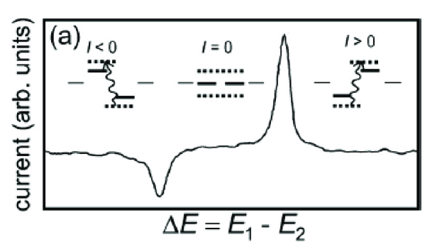
The relative position of the energy levels is
shifted by the gate voltage in the figure. The central
peak corresponds to elastic tunneling while the satellite
resonances involve the emission (left satellite) or absorption
(right satellite) of one photon. The slight asymmetry of the
central resonance at large negative gate voltages can be
understood in terms of relaxation processes due to emission of
phonons. In the large bias voltage configuration, these relaxation
processes contribute also to the current. This is the case even
for very low temperatures when spontaneous emission of phonons
always gives a contribution to the current for [241] . By increasing the microwave frequency, the
distance between the main resonance and the satellites increases
linearly Fig. 59. b. This, as we will see below,
indicates the absence of quantum coherence between quantum dots.
By increasing the microwave power at fixed frequency (the
parameter in Eq. (218)), it is possible to
measure multiphoton processes. This is shown in Fig. 60
where absorption of multiple photons (up to 11 photons) is demonstrated.
The above theory has been extended in Ref. [256] to
include a coherent pumping mechanism via inelastic cotunneling
processes.
Importantly, by performing photon-assisted tunneling spectroscopy one is able to distinguish whether the two level system exhibits quantum coherence or not, as we shall discuss in the next subsection.
11.3 Photon-assisted tunneling in strongly coupled double quantum dots
An increase of the interdot tunneling coupling delocalizes the electron wave function over the entire double dot structure. Provided that the simplified two-level picture is correct, elementary quantum mechanics tells us that the new eigenstates of this problem are now the symmetric (bonding) and antisymmetric (antibonding) combinations of the localized states. The new eigenvalues are expressed in terms of the energies of the uncoupled states as:
| (219) |
such that .
We have described photon-assisted tunneling spectroscopy in weakly coupled quantum dots. The next natural step would be to use this technique to study strongly coupled dots in order to investigate quantum coherence across the double dot system. This is not an easy task though. As we mentioned, relaxation processes due to spontaneous emission always contribute to the current for [241] . With increasing the interdot tunneling coupling between dots the spontaneous emission rate also increases which renders the large bias voltage configuration unapropriate to study the strong coupling regime. This difficulty can be overcome by using the pumping configuration, the advantage being that relaxation processes can lower the current but do not contribute to it. An example of pumped current due to photon-assisted tunneling in this configuration is given in Fig. 61. The positive peak corresponds to pumping electrons from the left to the right dot () while the negative one corresponds to the opposite effect when . The central resonance is absent because the bias voltage is zero.
When the interdot tunneling coupling is strong enough, the formation of the bonding and antibonding states results in a new condition for observing a pumped photon-assisted tunneling current: to promote electrons from the low energy state to the high energy state one needs now microwaves of frequency:
| (220) |
Eq. (220) can be rewritten as:
| (221) |
This has to be compared with the condition for weak coupling which is:
| (222) |
From the previous reasoning, it is thus obvious that if one measures the pumped photon-assisted tunneling current through a double quantum dot in the strong coupling regime the position of the peak (antipeak) at positive (negative) should follow the hyperbolic form given by Eq. (220) instead of the linear relation in Eq. (222).
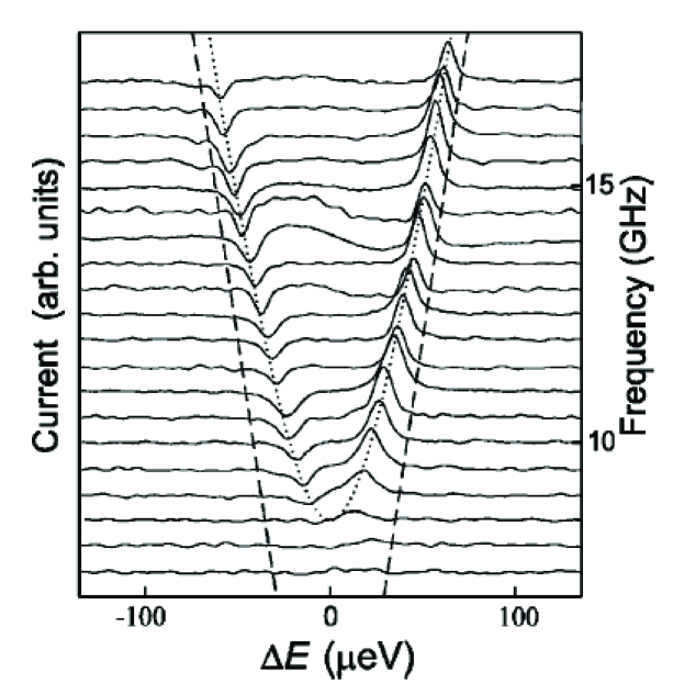
This was experimentally demonstrated by Oosterkamp et al in Ref. [249]. They measured the pumped current as a function of the uncoupled energy difference for different microwave frequencies and showed that indeed the position of the resonances deviates from the linear relation in Eq. (222) when is fixed and . These results are presented in Fig. 62.
Similarly to the weak coupling case, the Rabi frequency becomes renormalized by the microwave field. In this case, such that the interdot tunneling coupling renormalizes as, see Eq. (11):
| (223) |
Namely, a strong microwave field reduces the tunnel coupling such that the condition for pumping becomes:
| (224) |
11.4 Spin-polarized pumps
Cota et al recently followed up the ideas described in section 11.1 in order to investigate pumping of spin-polarized electrons [257]. Interestingly, the application of ac voltages allows to control the degree of polarization of the current flowing through a double quantum dot even in the case where the contact leads are not spin polarized. This is of importance, for understanding and controlling the behavior of spins in nanostructures has become the subject of intense investigation due to its relevance to quantum information processing and spintronics [258].
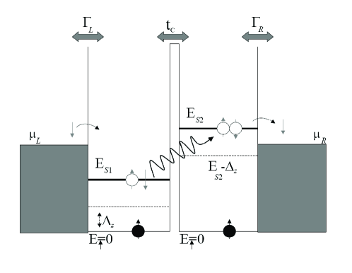
An schematic diagram of the operation principle of the spin-pump proposed in Ref. [257] is shown in Fig. 63. and are the energies of the doubly occupied states in each dot, with a Zeeman splitting on both dots (it is assumed that the leads are unpolarized). The frequency of the ac field is tuned such that . Preparing the system initially in the state (or in the state which is immediately filled by a electron when ), pumping of spin is obtained in the regime where the chemical potential for taking electrons out of the right dot fulfils while the chemical potential for taking electrons out of the right dot fulfils . Then, a spin-polarized pump is realized through the sequence: or which involve states of double occupation on both dots.
The above qualitative explanation can be substantiated by studying the problem with a reduced density matrix, see Eq. (214), fully taking into account the dynamics of a Hilbert space comprising the sixteen states: , , ,, , ,, ,, , , , , . To account for intrinsic decoherent processes acting even in the isolated system, a term is added to in Eq. (214) for terms involving spin-flips. Typically, is at least an order of magnitude smaller than , the spin relaxation time 272727Recent experiments on vertical quantum dots measured typical relaxation times [259]. The observed relaxation time can be understood by inelastic cotunneling. Spin-orbit interactions are also predicted to give an important contribution to spin relaxation in GaAs quantum dots [260].. is given by , where and are spin-flip relaxation rates, such that . These spin-relaxation rate terms are taken into account in the evolution equations (214) for the diagonal elements of the reduced density matrix.
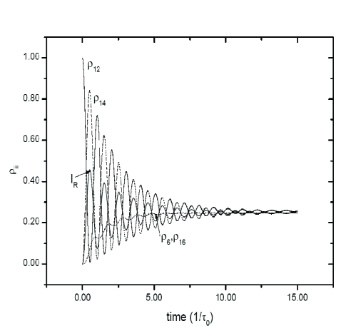
An example from this calculation is shown in Fig. 64 where the dynamics of the relevant density matrices , , and , (for convenience we use the notation ) is plotted. The current to the right lead, which is given by the expression:
| (225) | |||||
is also plotted. After a few periods of the Rabi oscillation, both a steady-state polarized current and a finite population of the states and are reached demonstrating the efficiency of the pump.
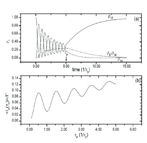
Further insight into the dynamics of the pump can be gained by studying pulsed ac fields. As shown experimentally [261, 262] and theoretically [256, 263], by applying a short pulse via a gate electrode, Rabi oscillations can be resolved and observed through current measurements. This is an important example of the possibility of observation and control of coherent quantum state time evolution. Importantly, it is crucial for the system to be able to return to the initial (ground) state after the pulse has been turned off. This is shown in Fig. 65 where the system is initially prepared in state , a pulsed ac field (duration of the pulse ) is applied and then the system is let to evolve for a time (Fig. 65(a)). We see, from the time evolution of the density matrix elements that the Rabi oscillations are clearly resolved for , and that the system eventually regains the initial ground state () after the field is turned off. Next, by applying pulses of different length in sequence, one can calculate the time-averaged current to the right lead . The results (Fig. 65(b)) show that the Rabi oscillations of spins between the two quantum dots can be clearly resolved and observed through current measurements.
Note that in the above set-up, states of double occupancy in each dot play a decisive role in obtaining the spin-polarized pumping mechanism with unpolarized leads. Indeed, if the configuration is such that states of doubly occupancy in both dots are above the chemical potentials in the leads (such that only states with up to two electrons in the double dot are relevant) the pump becomes ineficcient: Let us assume that one starts from the state , the ac field is tuned to resonance and the pumping mechanism starts to populate the state . Very rapidly, the spin-triplet state will dominate the dynamics because the state is unavailable. As a consequence, the total current eventually goes to zero for and 282828This spin blockade of the current due to the Pauli exclusion principle has been observed in weakly coupled double dot systems by Ono et al [264].. In other words, the appearance of the triplet blocks the pumping characteristics of the system, due to the Spin Blockade effect. This result is general, with growing with time more or less rapidly depending on the parameters of the problem292929A spin-pump with two electrons in the double dot has been proposed very recently by Sun et al in Ref. [265]. Here a rather stringent condition, a spatially nonuniform magnetic field in the double dot system, is needed such that the ground state in the double dot system is instead of ..
11.5 Photon-assisted tunneling in strongly dissipative double quantum dots
As mentioned in section 11.2, the current in the large bias voltage configuration has always an inelastic contribution that can be understood in terms of relaxation processes due to emission of phonons. This is the case even for very low temperatures when spontaneous emission of phonons always gives a contribution to the current for [241]. The effect of a phonon bath on the transport properties of double quantum dots in the low bias voltage regime has been investigated experimentally by Qin et al [266].
In the presence of a generic dissipative bosonic bath (), the Hamiltonian of Eq. 215 becomes:
| (226) |
The effects of the bosonic bath are fully encapsulated in a spectral density
| (227) |
where are the frequencies of the bosons and the denote interaction constants. The Hamiltonian of Eq. (226) is known in the literature as the driven spin-boson Hamiltonian303030The driven spin-boson Hamiltonian has been studied extensively during the last years in the context of quantum dissipative systems. For further details, we refer the reader to the review by Grifoni and Hänggi in Ref. [10]..
The coupling to external reservoirs is again described by Eq. (216). In the presence of the bosonic bath, Eqs. (217) describing the reduced density matrix are modified as follows:
The boson correlation function for a harmonic bath with spectral density , Eq. (227), and at equilibrium temperature enters as,
| (229) |
Without driving, , Eqs. (11.5) were solved by Brandes and Kramer [267]. The stationary current without ac reads:
| (230) |
with
and , where denotes the Laplace transform:
| (231) |
is obtained by expanding Eq. (230) to lowest order in , namely:
| (232) |
In the driven case, the stationary current to lowest order () reads [268]:
| (233) |
Remarkably, Eq. (233) is given by a Tien-Gordon formula for arbitrary electron-boson coupling: the current in the driven system is expressed by a sum over current contributions (including the coupling to the dissipative bosonic bath) from side-bands , weighted with squares of Bessel functions. Explicitly,
| (234) |
11.6 Floquet theory for investigating ac-driven quantum dots
Ever since the pioneering work of Anderson [269], it has been known that random spatial disorder can cause electronic states to become localised in quantum systems. As we have discussed in previous sections, it has been found recently that an ac driving field can produce a similar intriguing effect termed dynamical localisation, in which the tunneling dynamics of a particle can be destroyed. One of the first systems in which this effect was predicted is that of a particle moving in a double-well potential [11]. A physical realization of this could consist of two coupled quantum dots containing a single electron — the simplest type of artificial molecule possible. If this system is prepared with the electron occupying one of the quantum dots, one can expect it to tunnel across to the other quantum dot on a time scale set by the Rabi frequency. However, if an ac field of the correct strength and frequency is applied to the system, the tunneling is destroyed, and the particle will remain trapped in the initial well.
Weak time-dependent fields are generally treated as small perturbations, which produce transitions between the eigenstates of the unperturbed quantum system. This approach, however, is not applicable to treat the strong driving fields required to produce dynamical localisation, and instead the technique of Floquet analysis [10], which is valid in all regimes of driving, has proven to be extremely effective. In this approach, the important quantities to calculate are the quasi-energies, which play a similar role in driven systems to the eigenenergies in the undriven case. In particular, dynamical localisation occurs when two quasi-energies of states participating in the dynamics approach each other, and become either degenerate (a crossing) or close to degenerate (an avoided crossing). Using this formalism, analytic and numerical studies of the double-well system have shown [15, 16, 223] that in the limit of high frequencies, quasi-energy crossings occur when the ratio of the field strength to the frequency is a root of the Bessel function . Adding a second electron to the coupled quantum dot system, however, introduces considerable complications. At the low electron densities typically present in quantum dots, strong correlations produced by the Coulomb interaction can significantly influence the electronic structure. One of the most dramatic consequences of this is the formation of Wigner molecule states [270] that will be discussed in subsection 12.3. Understanding the interplay between electron correlations and the driving field is, however, extremely desirable, as the ability to rapidly control electrons using ac fields [271] has immediate applications to quantum metrology [272], where a possible coherent turnstile device formed by a triple well operating in a picosecond time scale was proposed, and quantum information processing. In particular, manipulating entangled electrons on short timescales is of great importance to the field of quantum computation [273]. These kind of problems can be studied by applying the Floquet formalism to systems of interacting particles. We illustrate this by describing a system of two interacting electrons confined to a pair of coupled quantum dots. A consequence of the interaction is that the system only responds strongly to the field when the frequency is in resonance with the Coulomb interaction energy, namely . When this condition is satisfied, CDT, which in this case is governed by the roots of higher-order Bessel functions (order ), can occur.
11.6.1 The driven double quantum-dot: a three-level system
Here we describe a simplified model of a double quantum dot, in which each quantum dot is replaced by a single site. Electrons are able to tunnel between the sites, and the effect of interactions is included by means of a Hubbard- term. This simple model captures all the main physics originating from the interplay between strong ac driving and electronic correlations. The Hamiltonian of this simplified system reads [17, 19]:
| (235) |
Here is the hopping parameter, and for the remainder of this discussion we shall take , and measure all energies in units of . is the external electric potential applied to site . Clearly only the potential difference, , is of physical importance, so one may choose to take the symmetric parametrization:
| (236) |
The Hilbert space of Hamiltonian (235) is six-dimensional, comprising three singlet states and a three dimensional triplet space. Measurements on semiconductor quantum dots have shown that the spin-flip relaxation time is typically extremely long [259], and so it is a good starting point to neglect spin-flip terms in the Hamiltonian. Consequently the singlet and triplet sectors are completely decoupled, and so if the initial state possesses a definite parity this will be retained throughout its time-evolution, and only states of the same parity need to be included in the basis.
The time evolution of this model system [17] already contains the main physics obtained from more complicated approaches like full simulations of detailed physical model of two interacting electrons confined to a pair of coupled GaAs quantum dots [17, 272, 274]. A great deal of information can be extracted from the time evolution of the probability functions , and , which are respectively the probability that both electrons are in the left quantum dot, both are in the right quantum dot, and that one electron is in each of the quantum dots:
| (237) |
The Coulomb interaction favors separating the electrons, and thus for strong interactions the ground-state has a large value of , and relatively small values of and . In Fig. 66 the time evolution of these quantities for and , at two different values of electric potential are plotted [17]. The ground state of the static Hamiltonian is used as the initial state. It is the dynamics of the ground state, i.e., the singlet which is interesting because the electronic configuration will oscillate between single and double occupation of the quantum dots. In both cases the detailed form of the time-evolution is highly complicated, but it is clear that the system behaves in two distinct ways. In Fig. 66a the value of periodically cycles between its initial high value (indicating that each dot holds approximately one electron) to nearly zero, while the values of and correspondingly rise and fall at its expense. This behavior is very different to that shown in Fig. 66b, where never drops below a value of 0.78, and the other two probabilities oscillate with a very small amplitude. It thus appears that CDT is occurring in the second case, and that the system’s time evolution is essentially frozen. If one terms the minimum value of attained during the time-evolution , one can use this to quantify whether CDT occurs, as a high value of signifies that tunneling has been destroyed, while a low value indicates that the electrons are free to move between the quantum dots.

This is illustrated in Fig. 67b where a contour plot of
as a function of both of the frequency and strength of
the ac field is presented. Dark areas correspond to low values of
, and it can be seen that they form horizontal bands,
indicating that the system is excited strongly by the ac field
only at “resonant” values of . Close examination of this
plot reveals that these bands occur at frequencies , at which the system can
absorb an integer number of photons to overcome the Coulomb
repulsion between electrons, thereby enabling tunneling processes
such as to occur. We can additionally observe
that these bands are punctuated by narrow zones in which CDT
occurs. Their form can be seen more clearly in the cross-section
of given in Fig. 68a, which reveals them to be
narrow peaks. These peaks are approximately equally spaced along
each resonance, the spacing increasing with . Another
contour plot of is shown in Fig. 67a, this
time obtained from a full simulation of two interacting electrons
confined to a pair of coupled GaAs quantum dots [17]. The
striking similarity between these results clearly indicates that
the simple, effective model (235) indeed captures the
essential processes occurring in the full system.
Tamborenea et
al [274] performed a full numerical simulation
of the two particle Schrödinger equation considering the configuration
interaction. Their results were similar to those presented in
Fig. 67a, which correspond to a numerical integration of
the Schrödinger equation by Creffield et al [17].
However there is an important difference which comes from the
larger sample size considered in [274]. The narrower structure
studied in [17] (Fig. 67a)
allows finer detail to be shown, and
to resolve the punctuated regions of the bands in which CDT occurs
and in which the system remains localized in its initial state.
These regions are fundamental
to describe the two electron dynamics for different intensities
and frequencies of the ac field.
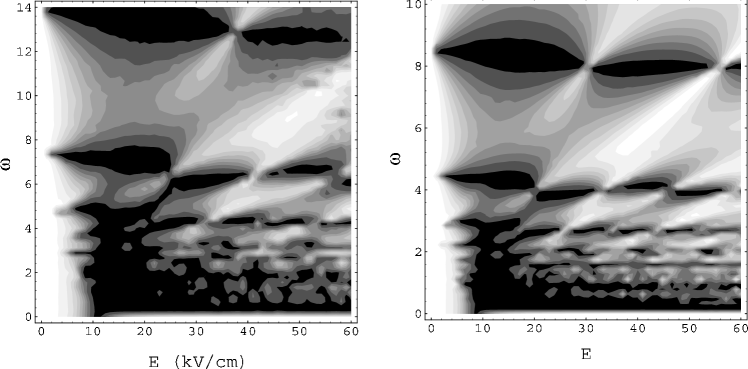
These results are radically different to those obtained for non-interacting particles. In this case an analogous plot of delocalisation shows a fan-like structure [16], in which localisation occurs along lines given by , where is the -th root of the Bessel function .
In Fig. 68a the Floquet quasi-energies as a function of the field strength for , one of the resonant frequencies visible in Fig. 67b, are shown. We see that the system possesses two distinct regimes of behavior, depending on whether the driving potential is weaker of stronger than . For weak fields , as studied previously in Ref. [275], the Floquet spectrum consists of one isolated state (which evolves from the ground state) and two states which make a set of exact crossings. Although in this regime shows little structure, these crossings do in fact influence the system’s dynamics. This is demonstrated in Fig. 69 where the Floquet quasi-energies in the weak-field regime for the case of are plotted. Beneath, the minimum value of attained during the time-evolution is shown (where this time the state has been used as the initial state). It can be seen that for this choice of initial condition, the crossings of the quasi-energies again produce CDT and freeze the initial state — despite the Coulomb repulsion between the electrons. This surprising result may be understood as follows. For large values of , the singlet eigenstates of the undriven system consist of the ground state, separated by the Hubbard gap from two almost degenerate excited states. For small values of the driving potential, the two excited states remain isolated from the ground state, and constitute an effective two-level system with a level-splitting of . Thus if the system is prepared in an initial state which projects mainly onto the excited states, its dynamics will be governed by the two-level approximation [15, 16, 223], and CDT will occur at the roots of . We show in Fig. 69a the quasi-energies obtained from the two-level approximation, which give excellent agreement with the actual results with no adjustable parameters. As becomes comparable to the Hubbard gap, however, the two excited states are no longer isolated from the ground state, and all three levels must be taken into account. This can be seen in the progressive deviation of the quasi-energies from the two-level approximation as the electric potential approaches [276].
When the electric potential exceeds , the system displays a very different behavior, in which remains close to zero except at a series of narrow peaks, corresponding to the close approaches of two of the quasi-energies. A detailed examination of these approaches (see Fig. 68b) reveals them to be avoided crossings between the Floquet states which evolve from the ground state and the higher excited state, and have the same generalized parity. The remaining state, of opposite parity, makes small oscillations around zero, but its exact crossings with the other two states do not correlate with any structure in .

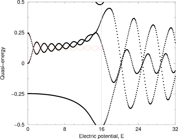
To interpret this behavior in the strong-field regime, one can obtain analytic expressions for the quasi-energies via the perturbation theory described in Subsection 3.1. The first step is to solve the eigenvalue equation, see Eq. (12), in the absence of the tunneling component . In a real-space representation the interaction terms are diagonal, and so it can be readily shown that an orthonormal set of eigenvectors is given by:
| (238) |
Imposing -periodic boundary conditions reveals the corresponding eigenvalues (modulo ) to be and . These eigenvalues represent the zeroth-order approximation to the Floquet quasi-energies, and for frequencies such that all three eigenvalues are degenerate. This degeneracy is lifted by the perturbation , and to first-order, the quasi-energies are obtained by diagonalizing the perturbing operator . By using to rewrite the form of , the matrix elements of can be obtained straightforwardly:
| (239) |
and its eigenvalues
subsequently found to be and (the matrix elements and eigenvalues are given
in units of the interdot hopping t), where . For the non-interacting case U=0, the solution for independent electrons is recovered:
.
Fig. 68a demonstrates the excellent agreement between this
result (with ) and the exact quasi-energies for strong and
moderate fields, which allows the position of the peaks in
to be found by locating the roots of . Similar
excellent agreement occurs at the other resonances. For weak
fields, however, the interaction terms do not dominate the
tunneling terms and the perturbation theory breaks down, although
we are still able to treat the system phenomenologically by using
an effective two-level approximation.
Zhang et al., considered as well a Hubbard type model to study the dynamics of two interacting electrons in double quantum dots [275, 277, 278]. They numerically analyzed the character exchange of the Floquet states at avoided triple crossings which appears in a three level system as a function of the field intensity in the neighborhood of an avoided crossing. They observed that the degree of CDT at the avoided crossings depends on the exchange of character between the three participating states.
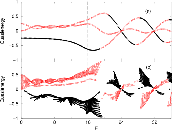
Recent calculations [279] study the dynamics of two interacting electrons in quantum dot arrays driven by ac-fields. In this system also two different regimes are found as a function of the ratio between the strength of the field and the inter-electron Coulomb repulsion. When the ac field dominates, CDT occurs at certain frequencies , in which transport along the array is suppresed. In the other limit: weak driving regime, an interesting result is found: the two electrons can bind into a single composite particle - despite of the strong Coulomb repulsion between them, which can then be controlled by the ac field. These results can be explained in terms of the quasienergy spectrum [279]. In particular, these two regimes of weak and strong driving are a generic effect and the effects seen in a two-site system arise in an analogous way such as the two intercrossing quasienergies in the weak driving regime are replaced by a miniband of states. This is illustrated in Fig. 70 where the quasienergy spectrum for a two-site system and a sixteen-site system are compared.
12 Photon assisted tunneling in quantum dots II: strongly correlated quantum dots
12.1 Beyond the Coulomb blockade: Kondo effect
12.1.1 Basics
So far, we have restricted ourselves to describe transport in the sequential regime, namely transport to lowest order in the coupling to the reservoirs. This is not the only contribution though: under certain conditions higher-order tunneling processes become more and more relevant as the resistance of the tunneling barriers approaches the quantum of resistance .
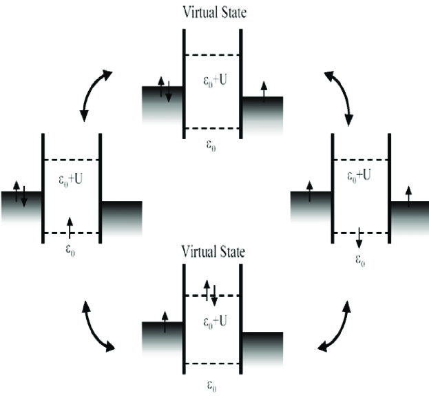
In this situation, quantum fluctuations dominate transport because electrons are allowed to tunnel via intermediate virtual states where first order tunneling would be supressed. Thus, the intrinsic width of the energy levels of the quantum dot does not only include contributions from direct elastic tunneling but also tunneling via virtual states. These higher-order tunneling events are referred to as cotunneling processes. Experimental results on cotunneling in semiconductor quantum dots have been reported in Refs. [280, 281, 282, 283]. Photon assisted tunneling in the cotunneling regime has been studied theoretically by Flensberg in Ref. [284], but, to our knowledge, no experiments in this regime exist to date.
Higher-order tunneling events lead to spectacular effects when the spin of the electrons is also involved: a quantum dot with a net spin coupled to electron reservoirs resembles a magnetic impurity coupled to itinerant electrons in a metal and, thus, can exhibit Kondo effect. The Kondo effect appears in dilute alloys containing localized moments as a crossover from weak to strong coupling between itinerant electrons of the host non-magnetic metal and the unpaired localized electron of the magnetic impurity as the temperature is reduced well below the Kondo temperature () [285]. Due to spin exchange interaction, see below, the conduction electrons tend to screen the non-zero spin of the magnetic impurity such that a many-body spin singlet state, consisting of the impurity spin and the itinerant electrons surrounding the impurity, forms.
As we mentioned, a quantum dot with a net spin and coupled to reservoirs mimics the above situation. In the simplest model of a magnetic impurity, the Anderson model, there is only a single spin degenerate level coupled to itinerant electrons. The same situation applies for quantum dots with an odd number of electrons (only the topmost level which can accomodate a spin up or down is considered) 313131This is not the only situation where Kondo effect can appear in quantum dots. For other examples where the Kondo effect appears for an even number of electrons in the quantum dot see Refs. [286, 287, 288, 289, 290, 291].. The role of the itinerant electrons in the usual Anderson model is played here by the electron reservoirs to which the quantum dot is coupled to. Fig. 71 (left) shows a schematic diagram of the energy profile of a quantum dot using the language of the Anderson model. A quantum dot with an odd number of electrons can be represented by the topmost occupied level which is below the Fermi energy of the leads and is occupied by a spin (up in the figure). Adding another electron to the quantum dot costs a charging energy such that the double occupancy state has an energy well above the Fermi energy. On the other hand, it would at least cost to remove the electron from the dot. The Hamiltonian which describes this system is:
| (240) |
where each term of the total Hamiltonian is defined as follows
| (241) | |||
| (242) | |||
| (243) |
The operator creates an electron with spin in the quantum dot, while creates an electron in the reservoir with energy ( labels the rest of quantum numbers). is the coupling between the quantum dot and the reservoirs, which contributes to the intrinsic width of the energy levels of the quantum dot with
| (244) |
where is the hybridization single-particle retarded self-energy, see below. In the simplest case (wideband limit) one neglects the principal value of the hybridization self-energy and consider the imaginary part to be an energy independent constant, i.e., , where is the electron density of states in the leads.
To lowest order, the transport in the Coulomb blockade region is inhibited because . Nonetheless, quantum uncertainty allows the system to visit classically forbidden virtual states (empty or doubly occupied) for a short period of time or , respectively (see middle graphs in Fig. 71). Within the short timescale another electron must tunnel to the dot (if the virtual state is the empty one) or out of the dot (if the virtual state is the doubly occupied one). However, the initial and final states (left and right graphs in Fig. 71, respectively) may have opposite spins, namely the spin has flip. These spin flip processes can be described rigurously by an effective exchange Hamiltonian
| (245) | |||||
The local degree of freedom in the quantum dot is a spin () , where the components of are the Pauli matrices, and . The exchange Hamiltonian in Eq. (245) (together with a scattering term not shown here) is derived from the Anderson Hamiltonian by means of a canonical transformation (Schrieffer-Wolff transformation [285]) which integrates out the aforementioned virtual excited states. The exchange constant in this effective Hamiltonian can be written in terms of the original parameters as:
| (246) |
For symmetrical coupling to the leads one has which for is . Many spin flip events mediated by the exchange interaction in Eq. (245) lead to the formation of a many-body spin singlet state, consisting of the localized spin and the spins of the reservoirs. The energy scale for this singlet state is the Kondo temperature , where is a high energy cutoff. In the language of the Anderson Hamiltonian, the Kondo temperature reads This singlet is reflected in the local density of states (DOS) of the quantum dot as a narrow peak around : the Abrikosov-Suhl (AS) or Kondo resonance.
The Kondo effect leads to many remarkable properties and has been the subject of extensive research for decades in the context of metals with magnetic impurities [285]. In recent years, spectacular advances in nanotechnology have made it possible to experimentally study Kondo physics in quantum dots [292, 293, 294, 295, 296, 297]. These experiments confirm early theoretical predictions [298] that low-temperature transport through quantum dots in the Coulomb blockade regime should exhibit Kondo physics as described above. Kondo physics in quantum dots manifests as an increase of the linear conductance () as one lowers the temperature in regions with an odd number of electrons, which, again in the simplest case, corresponds to a net spin S=1/2.
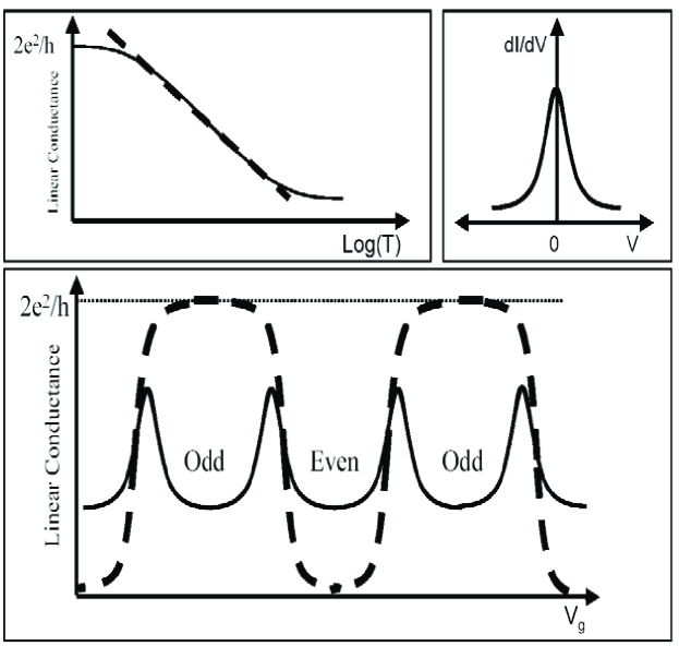
This linear conductance increase can be explained in terms of the increasing DOS around as one lowers the temperature, namely the Kondo resonance. For , the Kondo effect increases the linear conductance to its highest possible value . In other words, the spin-flip processes leading to the Kondo effect are able to make an otherwise Coulomb blockaded dot perfectly transparent. This limit of perfect conductance is called the unitary limit. Furthermore, the conductance, divided by its value at absolute zero, depends only on the temperature divided by , namely . Importantly, is an universal function such that the behavior of a system with parameters , , etc, depends only on : different systems with the same behave in an universal fashion. In bulk metals, the Kondo effect produces the opposite behavior, it decreases the conductance because in this case the scattering from magnetic impurities mixes electron states with different momenta which increases the resistance.
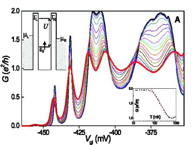
The main theoretical predictions of linear transport through quantum dots in the Kondo regime are schematically depicted in Fig. 72. Experimentally, linear transport through quantum dots in the Kondo regime was first studied in Refs. [292, 293, 294] and later in Refs. [295, 296, 297]. We show an example of these kind of experiments in Fig. 73 where we show the first demonstration of the unitary limit by van der Wiel et al [297]. In the nonlinear regime, the hallmark of the Kondo effect is a zero bias anomaly in the differential conductance as shown schematically in Fig. 72; an example from the experiments by Cronenwett et al [293] is shown in Fig. 74. Remarkably, quantum dots provide the possibility to control and modify the Kondo effect experimentally: the continuous tuning of the relevant parameters governing the Kondo effect [285] as well as the possibility of studying Kondo physics when the system is driven out of equilibrium, either by dc [299, 300, 301, 302, 303, 304] or ac voltages [305, 306, 307, 308, 309, 310, 311, 312, 313], which we shall discuss in the next subsection.
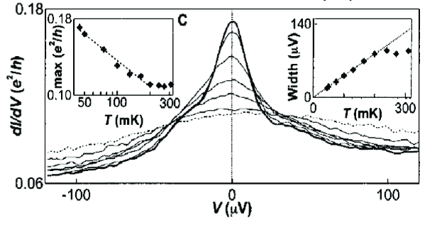
These kind of studies pave the way for the study of strongly correlated electron physics in artificial systems. Moreover, they provide a unique testing ground in which to investigate the interplay of strongly correlated electron physics, quantum coherence and non-equilibrium physics.
12.1.2 Kondo physics in quantum dots with ac driving: Introduction
Even before the first experimental demonstrations of Kondo effect in quantum dots, some papers addressed theoretically different aspects of the transport through ac-driven quantum dots in the Kondo regime [305, 306, 307]. These kind of studies are motivated by the possibility of studying Kondo physics in nonequilibrium situations not available in bulk metals. An ac potential can be applied to the central gate, , thus modulating the position of the energy levels of the quantum dot with respect to the leads. In this way, the ac potential can be used to periodically modify the Kondo temperature or to alternate between situations with strong spin fluctuations (Kondo regime) or charge fluctuations (mixed-valence regime). Alternatively, one may apply an ac bias to the leads.
As described in section 5, the linear transport through an ac driven quantum dot can be characterized by a time-averaged spectral density such that the linear conductance is given by [57]
| (247) |
where the time-averaged spectral density is defined as
| (248) |
and is the derivative of the Fermi function. The time dependent spectral density , with , is defined as the imaginary part of the Fourier transform with respect to of the retarded quantum dot Green’s function
| (249) |
Despite a considerable amount of work, the physical picture of the influence of microwaves on the Kondo conductance is still controversial. In the following, we mention some specific examples of theoretical work focusing on different aspects of the problem.
Goldin and Avishai [309] considered the case of a very strong ac bias with the help of third-order perturbation theory in the exchange constant. They concluded that the zero bias anomaly is supressed by the ac field and contains sidebands at multiples of the applied frequency. Furthermore, the zeroth and the first harmonics of the ac current are strongly enhanced by the Kondo effect while the other harmonics are small.
Nordlander et al., analyzed in Ref. [312] the effects of an ac voltage applied to the central gate by using a selfconsistent nonperturbative approach called non-crossing approximation (NCA) for calculating . They found a rich behavior of the conductance on the driving frequency and amplitude. At low frequencies a strong ac potential produces sidebands of the Kondo peak and a slow, roughly logarithmic, decrease of the linear conductance over several decades of frequency. The strength of the sidebands can be obtained analytically for the special case where a perturbative treatment in the tunneling coupling is appropriate. This limit can be better understood in terms of a time-dependent Kondo model which, with respect to properties near the Fermi level, is equivalent to the Anderson Hamiltonian. In this limit the dot can be replaced simply by a dynamical Heisenberg spin (), which scatters electrons both within and between reservoirs:
| (250) |
where the components of are the Pauli spin matrices. For near Fermi level properties, the relationship between the Kondo and Anderson Hamiltonians is for . Near the Fermi level, , which is the total rate at which lead electrons of energy undergo intralead and interlead scattering by the dot, has a Kondo peak. Furthermore, if is modulated as , then an electron scattered by the dot will be able to absorb or emit multiple quanta of energy , leading to satellites of the Kondo peak in . One can then obtain through the exact Anderson model relation
| (251) |
where is the state density per spin in the leads. The above can be illustrated explicitly using perturbation theory in . Keeping all terms of order and logarithmic terms to order one gets,
| (252) |
where , , , , and
| (253) |
the last limit being approached when . The coefficients are the strengths of the first satellites above and below a central peak of unit strength.
At high frequencies, photon-assisted tunneling processes result in a effective temperature such that even at zero temperature photon-assisted tunneling processes provides a cutoff for the Kondo singularity and reduce the conductance. Later, Kaminski et al pointed out in Refs. [310, 311] that even in the absence of dot ionization, low frequency microwaves are able to flip the spin of the dot, thus producing decoherence in the Kondo state. In Refs. [310, 311] only small frequencies and intensities were considered. In the following we describe a model by López et al [313, 314] where the Kondo effect in quantum dots with ac driving is studied for all ranges of ac parameters.
12.1.3 perturbative solution
The static Anderson model is exactly solvable [285] but a reliable method to obtain dynamical properties in the whole range of is not available. Some approximation is thus needed to evaluate the quantum dot retarded Green’s function in Eq. (248). For the NCA allows to study transport properties at intermediate temperatures . As we have described in the previous section, this is the route followed by Nordlander et al in Ref. [312]. Furthermore, the NCA method can be formulated in a fully time-dependent form such that non-equilibrium time-dependent properties of quantum dots in the Kondo regime can be studied [315]. NCA, however, breaks down as and does not recover properly the Fermi liquid regime. Other methods are thus called for. Second order finite U perturbation theory gives reliable qualitative results in the symmetric case but exhibits anomalies away from this special point. These anomalies can be circumvented by interpolating the selfenergy of order in order to achieve a proper behavior in the limits and and good analytic properties both, in and limits. In addition, charge conservation is obtained by introducing a selfconsistent parameter in this interpolative self-energy in order to fulfill the Friedel sum rule [301, 316]. This interpolative scheme was generalized to the ac case in Ref. [308]. In this work, the following ansatz for the quantum dot Green’s function in the presence of an ac potential is proposed
| (254) |
where is the static quantum dot retarded Green’s function. In Eq. (254) the ac potential breaks the symmetry under temporal translation only by introducing a global phase in the total quantum dot Green’s function. The physics of this ansatz is to assume that the only effect of the ac potential in the many-body state consists of flipping the quantum dot spin in a coherent way. Thereby using this ansatz one only accounts for coherent tunneling processes involving the absorption or emission of photons. As we shall see below, the neglect of inelastic tunneling processes, via multiphotonic events, is not a good approximation in many cases. From Eq. (254) one can obtain the time averaged Green’s function by Fourier transforming with respect to and performing the time average in the time variable
| (255) |
Here, is given by
| (256) |
where is the correlation self-energy obtained by the interpolative method with a Friedel sum rule which is generalized to the ac case [308]. depends on the time-averaged quantum dot occupation, , in the presence of ac potential
| (257) |
Using this model one obtains a DOS consisting of a Kondo peak at roughly weighted by and satellites at with weights . As a consequence the linear conductance departs from the unitary limit. As we shall see in the following, inelastic photon-assisted tunneling processes lead, in many cases, to a strong reduction of the central peak in the Kondo spectrum and therefore the linear conductance is strongly suppressed. Only in cases where the absorption and emission probability of photons is small (small ) do not contribute and the ansatz of Eq. (254) is a good approximation.
Within the context of perturbation theory in , the simplest extension that goes beyond the description given by the ansatz in Eq. (254) is just to calculate selfenergies to second order in without any assumption about how the breakdown of time-translational invariance modifies the propagators. Using the language of non-equilibrium Green’s functions (see Section 5) the second order self-energies read
| (258) |
and
| (259) |
| (260) |
The bare propagators in Eqs. (259,260) already include a Hartree correction, the coupling to the leads and the ac potential. In a first step, one calculates these propagators, without ac, including the Hartree contribution (given by , where is the quantum dot occupation) and the coupling to the leads:
| (261) |
Including the time modulation of the quantum dot level, the retarded and advanced quantum dot Green’s functions read:
| (262) |
Finally, the lesser and greater bare propagators can be obtained using
| (263) |
where are the lesser and greater coupling self-energies [57]. Finally, one can obtain the retarded Green’s function (to second order in ) solving the Dyson equation:
| (264) |
where =. This retarded Green’s function can be used in Eqs. (247,248,249) to calculate the linear conductance through the quantum dot[313].
12.1.4 Spin-flip cotunneling rate and average conductance
The main effect of the ac potential consists in a reduction of the time-averaged DOS at . This reduction can be interpreted as decoherence induced by ac excitations, either by real photon-assisted induced excitations at large ac frequencies [312] or virtual spin-flip cotunneling processes at small ac frequencies [310, 311]. These processes introduce a quenching of the Kondo peak causing a deviation of the linear conductance from the unitary limit. It is difficult to extract the magnitude of this lifetime induced by the ac potential from the analytical expressions above. Following Refs. [310, 311] a simple estimate for the lifetime can be obtained from the rate of spin-flip cotunneling. In the case of spin-flip cotunneling the simplest process involves the hopping of one electron out of the dot to a state above the Fermi level while another electron in the reservoirs, with opposite spin, enters into the dot. The rate of virtual spin-flip cotunneling which takes into account one photon processes is restricted to the case of very low ac frequencies and amplitudes, i.e., . Under these conditions the rate of spin-flip cotunneling was derived in Ref. [310, 311]. In the symmetric case the rate obtained there is zero. Without restrictions, the expression for the rate can be generalized quite easily [313]. By means of a modified Schrieffer-Wolff transformation [310, 311] one can obtain a Kondo Hamiltonian with a time dependent exchange constant,
| (265) |
To second order in the rate of spin-flip cotunneling can be found as
| (266) |
with
| (267) | |||||
In the limit of very low ac frequencies and taking into account one photon processes Eq. (267) reduces to the expression for the rate obtained in Ref. [311] by Kaminski et al:
| (268) |
Equation (265) shows that the rate of spin-flip cotunneling depends on the absorption or emission probability of photons through the Bessel functions, the energy denominators and the window of energy given by , its behavior as a function of the ac frequency depends on two opposite effects. On one hand, by increasing the window of allowed states becomes larger but on the other hand the absorption or emission probability diminishes. The competition of these two opposite effects produces a maximal rate at certain frequency .
These results can be connected with the results for the conductance obtained from Eqs. (247,248,249,12.1.3), by using an exact Anderson model relation for the scattering rate. In particular, the finite lifetime induced by the ac field reduces the scattering rate by introducing a finite lifetime (even at ). One can define an effective time-averaged self-energy in the presence of irradiation such that the time-averaged DOS at can be written as
| (269) |
The imaginary part of this effective self-energy can be identified as the total rate of decoherence induced by the ac potential, including the spin-flip cotunneling derived above, i.e.,
| (270) |
Both, the rate of spin-flip cotunneling and the total decoherence rate obtained from Eq. (270), present a non-monotonous behavior as a function of the external frequency with a maximum at .
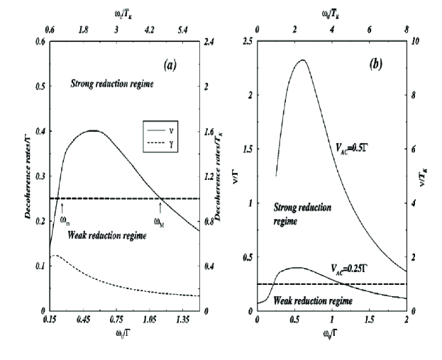
One example of this behavior is shown in Fig. (75) where the both rates as a function of are plotted. This dependence defines two different regimes for the problem: (i) weak reduction regime, which occurs when . In this case, the formation time for the Kondo state (given by [315]) is shorter than the necessary time to destroy it, which is given by the inverse of the decoherence rate, and the system spends most of the time in a Kondo state without or with little decoherence.
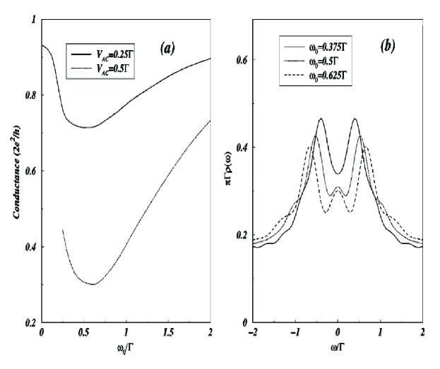
On average, this translates into a high linear conductance independently of the applied ac parameters. As long as the photon absorption or emission rate is negligible, and therefore the ac is not effective for inducing decoherence, it is irrelevant whether or not the frequency is larger or smaller than . (ii) strong reduction regime which is found when . In this case, the decoherence time is shorter than and the system spends most of the time in a state with a strong reduction of the Kondo effect.[313]
The results for the conductance are presented in Fig. 76a. As expected, the linear conductance behaves non-monotonously as a function of the external frequency with a minimum at . As a function of intensity, the linear conductance decays monotonously. At fixed , the maximum reduction of conductance occurs for the largest frequency (Fig. 76a, dotted curve).
The above results can be understood in terms of the average density of states (248). One example of such DOS is shown in Fig. 76b. Remarkably, the average DOS exhibits photon sidebands, namely replicas of the Kondo resonance, at . This result is in qualitative agreement with Refs. [305, 308, 309, 312]. Hence in an experiment one may also expect replicas of the zero bias anomaly, spaced by , in the differential conductance provided that the microwaves do not ionize the quantum dot. However, this is still an open question as we discuss in the next section.
12.1.5 Experiments
Experimentally, the effect of microwaves on the transport properties through quantum dots in the Kondo regime was studied by Elzerman et al [317]. In the entire frequency range studied (10-50 GHz) the Kondo resonance vanishes by increasing the microwave power such that no evidence of sideband formation is found.
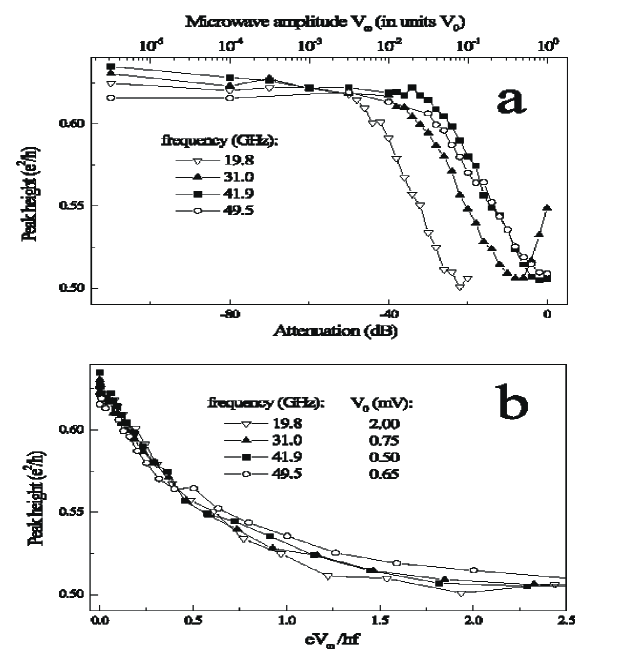
A possible explanation for the absence of sidebands is the extra source of decoherence induced by the finite dc voltage applied to measure the differential conductance . This extra source of decoherence which reduces the Kondo effect [310, 311] is not included in the calculations of Refs. [305, 308, 309, 312]. Concerning the linear conductance, the authors of the experiment in Ref. [317] conclude that the Kondo effect is reduced more effectively by microwave-induced dephasing than by temperature. Interestingly, they also find that the reduction of the linear conductance shows an scaling behavior, independently of , as a function of (Fig. 77), where is the estimated amplitude of the ac signal relative to the amplitude without attenuation . For each frequency, is estimated by comparing the onset of supression by microwaves, , with the thermal fluctuations .
12.2 Photon-assisted tunneling in one-dimensional quantum dots
The experimental realization of one-dimensional (1D) quantum wires has opened new possibilities to investigate electron transport in the presence of strong electron-electron interactions and impurities. For example, it has been possible to study Coulomb blockade through 1D islands created by random impurities in cleaved-edge-overgrotwth GaAs/AlGaAs quantum wires with low electron densities. The temperature dependence of the conductance through these systems showed, for the first time, clear evidence of non-Fermi liquid behavior. Contrary to the dc-transport case, where several theoretical works exist [318], the investigations of transport in 1D systems in the presence of ac fields are scarce. Furthermore, most of the theoretical work on ac-transport in Luttinger liquids focuses on the single barrier case [319, 320, 321, 322]. The photoconductance of a 1D quantum dot embedded in a non-fermi liquid has been studied by Vicari et al [323] by means of the bosonization technique. Motivated by the spin-charge separation in a Luttinger liquid, they consider spinless electrons such that only the collective low-energy charge density modes are relevant. These modes are described by the Hamiltonian:
| (271) |
Their quantization is described by the field operator and its conjugate . represents the long-wavelength part of the electron density , where is the mean electron density. is the constant that renormalizes the velocity of the charge modes due to interactions:
| (272) |
where is the Fourier transform of the 3D Coulomb interaction projected along the wire and is the Fermi velocity. The quantum dot is described by two symmetric delta-like barriers (amplitude and positions and , respectively), their presence induces -backscattering between left and right moving electrons such that the quantum dot is described in bosonized form as:
| (273) |
with . The unbalanced particles between left and right leads are described by , while describes the fluctuations of the particle number in the dot with respect to the mean electron number , such that the coupling to a time dependent gate voltage occurs through .
Vicari et al find that the photoconductance is strongly influenced by the strong electron interaction. At fixed temperature, the position of the sidebands does not depend on the interactions but their intensity is strongly reduced by decreasing (namely, increasing the interactions) from the non-interacting limit ().
As a function of temperature, the maxima of the sidebands peaks scale according to a non-Fermi liquid power law similar to the dc case:
| (274) |
Eq. (274) defines two regimes for the
conductance. In the weak interacting regime , the
conductance has a peak-like behavior which can be enhanced by
decreasing the temperature. On the other hand, in the strong
interactions regime the ac field is no longer able to
split the dc conductance in a series of sidebands. Note that this
is the characteristic behavior of metallic systems, namely for
strong interactions the quantum dot behaves as if it
had a continuous density of states
instead of a discrete one.
Finally, let us mention that although these theoretical
predictions have not been tested experimentally, the recent
experimental advances in the study of electron transport through
carbon nanotubes or cleaved-edge-overgrotwth GaAs/AlGaAs quantum
wires suggest that the observation of the above effects is not far
from reach. Importantly, these kind of experiments would allow to
study in a well controlled way high-frequency effects and ac
transport in non-Fermi liquid systems.
12.3 Wigner molecule regime in ac-driven quantum dots
As we have remarked during this chapter, the Coulomb interaction between the electrons can significantly affect the properties (transport, dynamics, etc) of a quantum dot. Such strongly correlated problems are notoriously difficult to treat, and the addition of a time-dependent field complicates the problem even further. When the mean inter-electron separation exceeds a certain critical value, however, a surprising simplification occurs, as the Coulomb interaction dominates the kinetic energy and drives a transition to a quasi-crystalline arrangement which minimizes the total electrostatic energy. In analogy to the phenomenon of Wigner crystallization in bulk two-dimensional systems [324, 325] such a state is termed a Wigner molecule [270]. As the electrons in the Wigner state are sharply localised in space, the system can be naturally and efficiently discretized by placing lattice points just at these spatial locations. A many-particle basis can then be constructed by taking Slater determinants of single-particle states defined on these lattice sites, from which an effective Hamiltonian of Hubbard-type can be generated to describe the low-energy dynamics of the system [326]. A major advantage of this technique over standard discretization [327, 328] schemes, in which a very large number of lattice points is taken to approximate the continuum limit, is that the dimension of the effective Hamiltonian is much smaller (typically by many orders of magnitude), which permits the investigation of systems which would otherwise be prohibitively complex. This approach has proven to be extremely successful in treating a variety of static problems, including one-dimensional quantum dots [326], two-dimensional quantum dots with polygonal boundaries [329, 330], and electrons confined to quantum rings [331, 332]. We further develop this method here by including a time-dependent electric field, and study the temporal dynamics of the system as it is driven out of equilibrium.
Let us consider a system of two electrons confined to a square quantum dot with a hard-wall confining potential — a simple representation of a two-dimensional semiconductor quantum dot. Such a system can be produced by gating a two-dimensional electron gas confined at a heterojunction interface, and by placing a gate split into four quadrants over the heterostructure [333], the potentials at the corners of the quantum dot can be individually regulated. In Fig.78a we show the ground-state charge-density obtained from the exact diagonalization of a square quantum dot [329], for device parameters placing it deep in the Wigner molecule regime. It can be seen that the charge-density is sharply peaked at four points, located close to the vertices of the quantum dot. This structure arises from the Coulomb interaction between the electrons, which tends to force them apart into diagonally opposite corners of the dot. As there are two such diagonal states, degenerate in energy, we can understand the form of the ground-state by considering it to be essentially a superposition of these two states (with a small admixture of higher energy states). The four points at which the peaks occur define the sites on which the effective lattice-Hamiltonian operates, as shown in Fig.78b.
Following Creffield et al in Ref. [18], one thus reduces the original problem to an effective lattice-Hamiltonian of the form:
| (275) |
Here represents the Coulomb repulsion between electrons occupying neighboring sites, and is the standard Hubbard- term, giving the energy cost for double-occupation of a site.
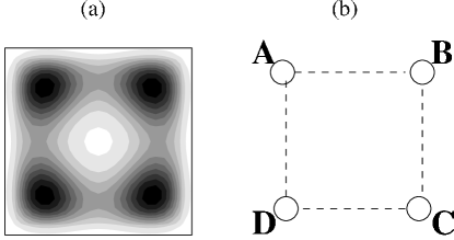
denotes the electric potential at site , which in general can have a static and a time-dependent component. In experiment, static offsets can arise either from deviations of the confining potential of the quantum dot from the ideal geometry, or by the application of gating voltages to the corners of the quantum dot. Applying corner potentials in this way would substantially enhance the stability of the Wigner molecule state, and could also be used to ensure that the multiplet of states included in the effective lattice-model is well-separated from the other excited states of the quantum dot system. In this discussion the effects of static gates are not explicitly considered. Also, the influence of small, accidental offsets encountered in experiments is neglected as they are expected to have only minor effects, and indeed may even stabilize CDT [14]. For convenience, we consider applying an ac field aligned with the -axis of the quantum dot, which can be parameterized as:
| (276) |
where A,B,C,D label the sites as shown in Fig.78b. We emphasize that although we have the specific system of a semiconductor quantum dot in mind, the effective-Hamiltonian we are using can describe a wide range of physical systems, including arrays of connected quantum dots [334], and our results are thus of general applicability.
As for the case of the double quantum dot in Section 11.6, no spin-flip terms in (275) are included and so the singlet and triplet sectors are again decoupled. Initial states with singlet symmetry are chosen, which corresponds to the symmetry of the system’s ground-state. Simple state counting reveals that the singlet sector has a dimension of ten, and can be spanned by the six states shown schematically in Fig.79, together with the four states in which each site is doubly-occupied.

12.3.1 Interacting electrons, double occupancy excluded
If the Hubbard- term is taken to be infinitely large one works in the sub-space of states with no double occupation. The Hilbert space is thus six-dimensional, and one can use the states shown in Fig.79 as a basis. We show in Fig.80 the time-dependent number occupation of the four sites at two different values of , in both cases using state as the initial state, and setting the ac frequency to . In Fig.80a has a value of 100.0, and it can be clearly seen that the electrons perform driven Rabi oscillations between the left side of the quantum dot and the right. Accordingly, the occupation number of the sites varies continuously between zero and one. In Fig.80b, however, we see that changing the electric potential to a value of produces dramatically different behavior. The occupations of sites A and D only vary slightly from unity, while sites B and C remain essentially empty throughout the time-evolution. Only a small amount of charge can transfer per period of the driving field between the left and right sides of the system, producing the small spikes visible in this figure. The amplitude of these features is extremely small, however, indicating that the tunneling between left and right sides has been almost totally destroyed.

A comparison of the amplitude of the oscillations of with the quasi-energy spectrum, as a function of the electric potential , indeed confirms that CDT is occurring, see Fig.81. Similarly to the double quantum dot system, we can see in Fig.81a that the quasi-energies have two different regimes of behavior. The first of these is the weak-field regime, , at which the driving field does not dominate the dynamics. In this regime the quasi-energy spectrum, and correspondingly, the amplitude of oscillations shows little structure. The second regime occurs at strong values of potential, , for which the quasi-energy spectrum clearly shows a sequence of close approaches. In Fig.81c an enlargement of one of these approaches is presented which reveals it to be an avoided crossing. Employing the perturbative method described in Section 3.1 demonstrates that the two quasi-energies involved in these avoided crossings are described by , where is equal to . We may thus again think of as signifying the number of photons the system needs to absorb to overcome the Coulomb repulsion between the electrons occupying neighboring sites. The results in Fig.81b and Fig.81d clearly show that the locations of the avoided crossings correspond exactly to quenching of the oscillations in , and so confirm that CDT indeed occurs at these points.

12.3.2 Interacting electrons, double-occupancy permitted
In the most general case one has to consider the competition between the and terms. Setting to a finite value means that the four doubly-occupied basis states are no longer energetically excluded from the dynamics, and accordingly the full ten-dimensional basis set has to be included.
Although it is difficult to obtain precise estimates for the values of parameters of the effective Hamiltonian, it is clear that in general . Accordingly, the parameters are chosen. Again, the frequency of the ac field is set to , and the quasi-energy spectrum obtained by sweeping over the field strength is studied [18], see Fig.82a. It is immediately clear from this figure that for electric potentials the form of the spectrum is extremely similar to the infinite- case. Performing perturbation theory confirms that, as in the previous case, the behavior of the quasi-energies is given by where . The amplitude of the oscillations of when the system is initialized in state is shown in Fig.82b which demonstrates that at the locations of the avoided crossings the tunneling parallel to the field is again quenched.

When the electric potential exceeds the value of , however, new structure appears in the quasi-energy spectrum. A group of four quasi-energies, that for weaker fields cluster around zero, become “excited” and make a sequence of avoided crossings as the field strength is increased. Perturbation theory predicts that these high-field quasi-energies are given by , where , and thus these avoided crossings arise when the absorption of photons equates to the electrostatic energy difference between the two electrons being on neighboring sites, and doubly-occupying one site. This then indicates that this structure arises from the coupling of the ac field to the doubly-occupied states.
To probe this phenomenon, the time evolution of the system from an initial state consisting of two electrons occupying site A is studied in Fig.83b. It can be seen that for electric potentials weaker than the amplitude of the oscillations in remains small, and shows little dependence on the field. As the potential exceeds , this picture changes, and the ac field drives large oscillations in , and in fact mainly forces charge to oscillate between sites A and B. At the high-field avoided crossings, however, the tunneling between A and B is suppressed, which shuts down this process. Instead, the only time-evolution that the system can perform consists of undriven Rabi oscillations between sites A and D, perpendicular to the field. As these oscillations are undriven they have a much longer time-scale than the forced dynamics, and thus during the interval over which we evolve the system the occupation of A only changes by a small amount, producing the very sharp minima visible in Fig.83b, centered on the roots of .

As the tunneling perpendicular to the field is undriven, it is straightforward to evaluate the time evolution of the initial state, if we assume that the left side of the quantum dot is completely decoupled from the right side: The occupation of sites A and D is then given by [18]:
| (277) |
where . For field intensities such that CDT occurs, the electron dynamics is restricted to the direction perpendicular to the applied field where Rabi oscillations take place. The decay of the amplitude of the Rabi oscillations as a function of time will indicate the degree of dynamical localization achieved for the particular field parameters considered [18]. If Rabi oscillations are damped, it will indicate that the isolation between the left and right sides of the quantum dot is not perfect. Tuning the parameters of the driving field therefore gives a simple and controllable way to investigate how a two-electron wavefunction can decohere in a quantum dot.
These results, together with those of Section 11.6, show that ac fields may not only be used as a spectroscopic tools to probe the electronic structure of a quantum dot systems, but can also be used to dynamically control the time-evolution of the system. The tunability of the CDT effect, and its ability to discriminate between doubly-occupied and singly-occupied states, make it an excellent means for rapid manipulation of the dynamics of strongly correlated electrons in mesoscopic systems.
13 Photon assisted shot noise
In a quantum conductor out of equilibrium, electronic current noise originates from the dynamical fluctuations of the current away from its average:
| (278) |
Shot noise, defined as the zero frequency limit of the power spectral density
| (279) |
provides us with a sensitive tool to study correlations between carriers. In particular, shot noise experiments reveal the charge and statistics of the quasiparticles relevant for electronic transport. Also, information about internal energy scales can be extracted from noise experiments323232For a detailed review about shot noise see Ref. [6].. For uncorrelated carriers with charge , (full shot noise or Poissonian noise). The Fano factor () quantifies deviations from the Poissonian noise.
Photon assisted shot noise was first observed by Schoelkopf et al [335]. They measured both dc transport and noise in a diffusive metallic conductor (namely, shorter than the electron phase-breaking length) irradiated by microwaves (=2-40GHz). Interestingly, their experiment demonstrates the first observation of photon assisted transport in a linear system: the dc conductance remains completely unafected by the microwaves in this linear mesoscopic system but the shot noise develops clear features associated with photon assisted transport. In particular, the differential shot noise shows steps at voltages corresponding to the photon energies . This behavior can be easily understood within the framework of scattering theory by noting that the shot noise of a coherent conductor can be written as [335, 336, 45]:
| (280) | |||||
where the ’s are the transmission probabilities of the different conduction channels of the conductor. For zero temperature, Eq. (280) develops singularities at voltages . The results of the experiments of Ref. [335] are presented in Fig. (84).
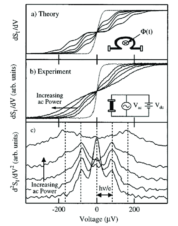
Very recently, a spectacular proof of photon assisted noise has been demonstrated. Reydellet et al [337] show experimentally that photon-assisted processes do generate shot noise even in the absence of net dc electron transport. This noise can be interpreted as generated by photon-created electron-hole pair partitioning. Without microwaves, noise in this mesoscopic system can be understood as follows: the left reservoir emits electrons at a frequency such that the incoming current is . Asuming a single mode with transmission probability , the transmitted current is and the conductance (Landauer formula). Shot noise originates from the quantum partition noise generated by electrons either transmitted or reflected. Quantum partition results in current fluctuations, bandwidth , . The binomial statistics of the partitioning is reflected in the factor [6]. The microwaves change the frequencies of the emitted electrons (as well as the probabilities of being emitted). In the limit one can define an effective noise temperature such that:
| . | (281) |
The first term represents thermal noise (Johnson-Nyquist) while the second one originates from photo-excited electron-hole pairs. When the modes are either fully transmitting or reflecting ( or ) there is no partition noise and only thermal noise contributes to Eq. (281).
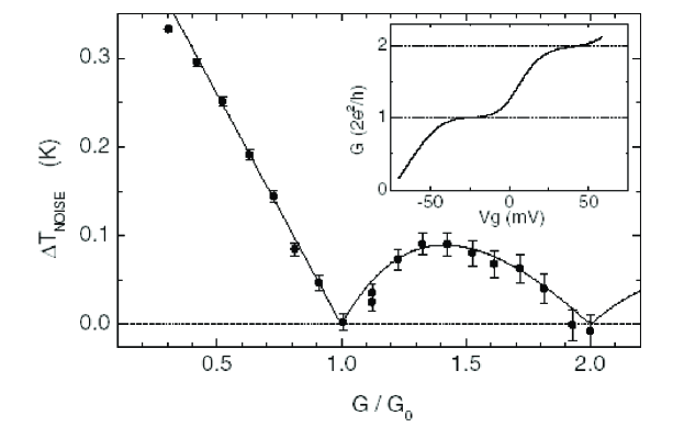
In intermediate situations, the noise temperature is proportional to the Fano factor which unambiguosly demonstrates photon-assisted partition noise as shown in the experiments of Ref. [337] (see Fig. (85)).
Theoretically, photon assisted shot noise has been also studied in the context of quantum dots by Sun and coworkers in Ref. [338] where they consider a single resonant state (without electron-electron interactions) coupled to leads (with time dependent voltages). When the broadening of the resonant state is smaller than , they conclude that the differential shot noise (at fixed dc voltage) versus gate voltage shows a resonant structure reminiscent of the sideband structure in the current versus gate voltage curves. When the system resembles the single-channel conductor studied by Schoelkopf et al [335] and the differential shot noise versus dc voltage shows a step-like behavior.
Recently, an extended theory of photon assisted shot noise has been put forward by Camalet et al [339]. They consider a generic situation where a multisite nanoscale conductor (without dissipation and electron-electron interactions) is coupled to leads. The Hamiltonian reads in a tight-binding approximation with orbitals
| (282) |
As usual, the leads are modeled by ideal electron gases, , where () creates an electron in the state () in the left (right) lead. The tunneling Hamiltonian, , establishes the contact between the sites , and the respective lead. The influence of an applied ac-field of frequency results in a periodic time-dependence of the Hamiltonian: such that a generalized Floquet approach for the evaluation of correlation functions can be developed. Here, we sketch the derivation.
The Heisenberg equations for the wire operators read
| (283) |
Within the wide-band limit approximation, the dissipative terms are memory free and the Gaussian noise , with , obeys
| (284) |
where denotes the Fermi function at temperature and chemical potential . Without the inhomogeneity, Eqs. (283) are linear with -periodic coefficients. Thus, it is possible to construct a complete solution with the help of a Floquet ansatz which in this case reads
| (285) |
The Floquet states obey the eigenvalue equation
| (286) |
where and . Note that the eigenvalue equation (286) is non-Hermitian (compare with Eq. (12)) in Section 3), its eigenvalues are generally complex valued and the (right) eigenvectors are not mutually orthogonal. Therefore, one needs to solve also the adjoint Floquet equation yielding again the same eigenvalues but providing the adjoint eigenvectors . It can be shown that the the Floquet states together with the adjoint states form at equal times a complete bi-orthogonal basis: and . For , both and reduce to the usual Floquet states.
The Floquet states allow to write the general solution of Eq. (283) in closed form. In the asymptotic limit , it reads
| (287) | |||||
The average current and the shot noise can be obtained from the closed form of the wire operators in Eq. (287). In particular, the shot noise reads:
| (288) | |||||
The retarded Green’s functions
| (289) |
describe the propagation of an electron from orbital to orbital .
Using Eq. (288), Camalet and coworkers study the noise properties of a simple wire with N=3 sites with equal energies and coupled to each other by a hopping matrix element . The on-site energies are modulated by an ac dipole field as , . is thus the electric field strength multiplied by the electron charge and the distance bewteen neighboring sites. Remarkably, they find that when both the dc current and the shot noise vanish (note that typically, as demonstrated experimentally by Reydellet and coworkers [337], a system with zero dc current is not noiseless). At current supression, the Fano factor exhibits a sharp maximum and two pronounced minima nearby. These results suggest that external ac fields could be used to obtain nanoscale devices with controllable noise levels. Note, however, that the above derivation neglects important effects like dissipation in the wire and electron-electron interactions.
14 Conclusions
In this review, we have attempted to give an overview of the physics of photon assisted tunneling in semiconductor nanostructures. Along the review, we have shown how the interplay of nonlinearity, time-dependent fields, electron-electron interactions and quantum confinement leads to new transport phenomena in nanostructures. During the last few decades, the study of these phenomena has lead to important developments in the fields of mesoscopic physics and nanoscience with a a wide scope ranging from the study of very basic concepts of quantum theory, like the demonstration of quantum coherence in artificial two level systems and the possibility of manipulating the dynamics of electrons in man-made structures, to engineering questions concerning ultimate speed limits of nanoelectronic devices.
A great deal of information can be extracted from simple models like the Tien-Gordon model. In particular, the key concept of photo side-bands and their physical meaning, namely that photon absorption () and emission () can be viewed as creating an effective electron density of states at energies with a probability given by , is already present in this simple description of photon assisted tunneling.
In many cases, more sophisticated theoretical tools are called for. Some of these tools, like The Floquet formalism, the non-equilibrium Green’s function technique or the density matrix technique, to name just a few, have been described in the review together with concrete applications to the study of the available experimental information. We have seen along the review how by using these theoretical techniques one can sed light on intriguing experimental observations like, for instance, the absolute negative conductance observed in THz irradiated semiconductor superlattices or the nontrivial features of photon-assisted transport through quantum dots in the Coulomb Blockade regime.
The use of these theoretical tools allows not only to explain experimental evidence but also to predict new effects which are not yet tested experimentally. Among these predictions we have described the possibility of realizing different electron pumps, including spin-polarized ones, by using ac fields, the coherent destruction of tunneling in artificial molecules, ac-induced sidebands of the Kondo resonance in the density of states of a strongly correlated quantum dot or the possibility of obtaining nanoscale devices with controllable shot noise levels by using ac fields, just to mention a few.
Although we have tried to present a review as exhaustive as possible, we are conscious that some of the topics covered along these pages would surely deserve a more in-depth treatment. We hope that the biased treatment of some topics, which obviously reflects the author’s views and partiality on some subjects, will be compensated by the reader’s desire of going deeply into little covered aspects (or even uncovered aspects we may have overlooked) of photon-assisted transport through semiconductor nanostructures.
We have provided many examples along the review which illustrate how one can obtain nontrivial physics by ac-driving a few electron system. Many important questions remain open, though. For instance, most of the calculations presented here study the response of the system to a field that is assumed to be known, but the actual field inside a few electron system can be rather different than the applied one due to interactions. Developments along this line are thus extremely desirable.
This is just an instance which demonstrates that, despite being rather mature, photon-assisted transport is still a very dynamic research area. We exemplify this with the last Sections of the review, photon-assisted tunneling in strongly correlated quantum dots and photon-assisted shot noise: two areas which, doubtlessly, will bring us new exciting developments in the coming years.
15 Acknowledgements
We greatly acknowledge the support of the Ministerio de Ciencia y Tecnología of Spain through the grant MAT2002-02465 (R. A. and G. P.) and the ”Ramón y Cajal” program (R. A.). We also thank the support of the EU through the RTN ”Nanoscale and Dynamics” HPRN-CT-2000-00144. During the last years we have benefited from collaborations and discussions with many colleagues, in particular, among others, Luis Bonilla, Tobias Brandes, Markus Büttiker, Valmir Chitta, Ernesto Cota, Charles Creffield, Silvano De Franceschi, Toshimasa Fujisawa, Leonid Glazman, Peter Hänggi, Jesús Iñarrea, Antti-Pekka Jauho, Sigmund Kohler, Leo Kouwenhoven, Bernhard Kramer, Rosa López, Jan Kees Maan, Miguel Moscoso, Tjerk Oosterkamp, David Sánchez, Carlos Tejedor, Sergio Ulloa, Mathias Wagner, Jürgen Weis and Wilfred van der Wiel. We also thank Markus Büttiker, Charles Creffield and Antti-Pekka Jauho for a critical reading of the manuscript.
References
- [1] A. H. Dayem and R. J. Martin, Phys. Rev. Lett. 8, 246 (1962).
- [2] P. K. Tien and J. P. Gordon, Phys. Rev. 129, 647 (1963).
- [3] V. A. Chitta, C. Kutter, R.E.M. de Bekker, J.C. Maan, S.J. Hawksworth, J.M. Chamberlain, M. Henini and G. Hill, J. Phys.: Condens. Matter, 6, 3945 (1994); V. A. Chitta, R.E.M. de Bekker, J.C. Maan, S.J. Hawksworth, J.M. Chamberlain, M. Henini and G. Hill, Surface Sci., 263, 227 (1992).
- [4] B.J. Keay, S. Zeuner, S.J. Allen, Jr., K. D. Maranowski, A. C. Gossard, U. Bhattacharya and M.J.M. Rodwell, Phys. Rev. Lett. 75, 4102 (1995).
- [5] W. G. van der Wiel, T. H. Oosterkamp, S. de Franceschi, C. J. P. M. Harmans, and L. P. Kouwenhoven, in Strongly Correlated Fermions and Bosons in Low-Dimensional Disordered Systems, eds. I.V. Lerner et al., 43 (2002), Kluwer Academic Publishers, The Netherlands.
- [6] Ya. M. Blanter and M. Büttiker, Physics Reports, 336, 1 (2000).
- [7] J. Bardeen, Phys. Rev. Lett.,6, 57 (1961).
- [8] John R. Tucker, IEEE Journal of Quantum Electronics, 15, 1234 (1979).
- [9] John R. Tucker and Marc J. Feldman, Rev. Mod. Phys. 57, 1055 (1985).
- [10] M. Grifoni and P. Hänggi, Phys. Rep. 304, 229 (1998).
- [11] F. Grossmann, T. Dittrich, P. Jung, and P. Hänggi, Phts. Rev. Lett. 67, 516 (1991).
- [12] B. V. Chirikov, F. M. Izrailev, and D. L. Shepelyansky, Physica D, 33, 77 (1988).
- [13] J. von Neumann and E.P. Wigner, Phys. Z 30, 467 (1929).
- [14] J. T. Stockburger, Phys. Rev. E, 59, R4709 (1999).
- [15] M. Holthaus, Z. Phys. B 89, 251 (1992).
- [16] F. Grossmann and P. Hänggi, Europhys. Lett. 18, 571 (1992).
- [17] C.E. Creffield and G. Platero, Phys. Rev. B 65, 113304 (2002).
- [18] C.E. Creffield and G. Platero, Phys. Rev. B 66, 235303 (2002).
- [19] C.E. Creffield and G. Platero in The Anderson transition and its ramifications-localization, quantum interference and interactions, ed. T. Brandes and S. Kettemann (Springer Verlag, Berlin, 2003).
- [20] H. Sambe, Phys. Rev. A 7, 2203 (1973).
- [21] R. Bavli and H. Metiu, Phys. Rev. Lett., 69, 1986 (1992).
- [22] M. Holthaus, Phys. Rev. Lett., 69, 1596 (1992).
- [23] Xian-Geng Zhao, J. Phys.: Condens. Matter 6, 4527 (1994).
- [24] M. M. Dignam and C. Martijn de Strerke, Phys. Rev. Lett., 88, 46806 (2002).
- [25] C. E. Creffield, Phys. Rev. B, 67, 165301 (2003).
- [26] J.C.A. Barata and W.F. Wreszinski, Phys. Rev. Lett. 84, 2112 (2000).
- [27] Marco Frasca, Phys. Rev. B, 68, 165315 (2003).
- [28] J. M. Villas-Boas, Wei Zhang, Sergio E. Ulloa, P.H. Rivera and N. Studart, Phys. Rev. B, 66, 85325 (2002).
- [29] M. Holthaus, Phys. Rev. Lett., 69, 351 (1992).
- [30] M. Holthaus and D. Hone, Phys. Rev. B, 47,6499 (1993).
- [31] A. A. Ignatov and Yu. A. Romanov, Phys. Status Solidi (b),73, 327 (1976).
- [32] A. A. Ignatov, E. Schomburg, K. F. Renk, W. Schatz, J. F. Palmier and F. Mollot, Annalen der Physik, 3, 137 (1994).
- [33] E. Schomburg, A.A. Ignatov, J. Grenzer, K. F. Renk, D. G. Pavel’ev, Yu. Koschurinov, B. Ja. Melzer, S. Ivanov, S. Schaposchnikov, and P. S. Kop’ev, Appl. Phys. Lett., 68, 1096 (1996).
- [34] D. D. Coon and H. C. Liu, Solid State Commun.,55, 339 (1985).
- [35] D.D. Coon and H. C. Liu, J. Appl. Phys. 58,6 (1985)
- [36] H. C. Liu, Phys. Rev. B, 43, 12538 (1991).
- [37] M. Wagner, Phys. Rev. B, 49, 16544 (1994).
- [38] M. Wagner, Phys. Rev. A 51, 798 (1995).
- [39] M. Wagner, Phys. Rev. Lett.,76, 4010 (1996).
- [40] M. Wagner and W. Zwerger, Phys. Rev. B, 55, R10220 (1997).
- [41] W. S. Truscott, Phys. Rev. Lett. 70, 1900 (1993).
- [42] W. C. Henneberger, Phys. Rev. Lett.,21, 838 (1968).
- [43] M. Buttiker and R. Landauer, Phys. Rev. Lett., 49, 1740 (1982).
- [44] E. H. Hauge and J. A. Stovneng, Rev. Mod. Phys., 61, 917 (1989).
- [45] M. H. Pedersen and M. Büttiker, Phys. Rev. B 58, 12993 (1998).
- [46] M. Büttiker, Phys. Rev. B 46, 12485 (1992).
- [47] M. Büttiker, A. Prêtre, and H. Thomas, Phys. Rev. Lett. 70, 4114 (1993).
- [48] M. H. Pedersen, S. A. van Langen and M. Büttiker, Phys. Rev. B 57, 1838 (1998).
- [49] H. Büttner and E. Gerlach, Phys. Lett. 27A, 226 (1968).
- [50] C. Caroli, R. Combescot, D. Lederer, P. Nozieres , and D. Saint-James, J .Phys. C 4, 2598 (1971).
- [51] C. Caroli, R. Combescot, P. Nozieres, and D. Saint-James, J. Phys. C 4, 916 (1971).
- [52] C. Caroli, R. Combescot, P. Nozieres, and D. Saint-James D., J.Phys. C. 5, 21 (1972).
- [53] R. Combescot, J. Phys. C 4, 2611 (1971).
- [54] L. Y. Chen and C. S. Ting, Phys. Rev. Lett. 64, 3159 (1990).
- [55] A. L. Yeyati and F. Flores, Phys. Rev. B 44, 9020 (1991).
- [56] Supriyo Datta and M. P. Anantram, Phys. Rev. B 45, 13761 (1992).
- [57] A.-P. Jauho, N. S. Wingreen and Y. Meir, Phys. Rev. B 50, 5528 (1994).
- [58] H. Haug and A.-P. Jauho, Quantum Kinetics in Transport and Optics of Semiconductors (Springer-Verlag, Berlin, 1996).
- [59] L. V. Keldysh, Zh. Eksp. Teor. Fiz. 47, 1515 (1965) [Sov. Phys. JETP, 20, 1018 (1965)].
- [60] L. P. Kadanoff and G. Baym, Quantum Statistical Mechanics (Benjamin, New York, 1962);
- [61] D. C. Langreth, in Linear and Nonlinear Electron Transport in Solids, Nato ASI, Series B vol. 17, Ed. J. T. Devreese and V. E. Van Doren (Plenum, New York, 1976).
- [62] Yigal Meir and Ned S. Wingreen, Phys. Rev. Lett., 68, 2512 (1992).
- [63] J. König and Y. Gefen, Phys. Rev. B 65, 045316 (2002).
- [64] J. Fransson, O. Eriksson and I. Sandalov, Phys. Rev. B 66, 195319 (2002).
- [65] C. A. Stafford, Phys. Rev. Lett. 77, 2770 (1996).
- [66] M. P. Anantram and S. Datta, Phys. Rev. B 51, 7632 (1995).
- [67] B. G. Wang, J. Wang, and H. Guo, Phys. Rev. Lett. 82, 398 (1999).
- [68] M. Büttiker, Y. Imry, R. Landauer, and S. Pinhas, Phys. Rev. B 31, 6207 (1985).
- [69] Tobias Brandes, Phys. Rev. B 56, 1213 (1997).
- [70] R. Meisels, F. Kuchar, J. J. Harris, and C. T. Foxon, Surface Science 263, 76 (1992).
- [71] G. M. Sundaram et al., in ICTP–NATO Workshop on Quantum Dynamics, Vol. 291 of Nato ASI Series, edited by H. Cerdeira, B. Kramer and G. Schön (Kluwer Academic Publishers, Dordrecht/Boston/London, 1994), p. 371.
- [72] R. Meisels et al., in NATO Advanced Study Institute, Bad Lauterberg, Vol. 326 of Nata ASI Series E, edited by B. Kramer (Kluwer Academic Publishers, Dordrecht, 1996).
- [73] R. Tsu and L. Esaki, Appl. Phys. Lett. 22, 11 (1973).
- [74] V.J. Goldman, D.C. Tsui and J.E. Cunningham, Phys. Rev. Lett. 58, 1256 (1987).
- [75] V.J. Goldman, D.C. Tsui and J.E. Cunningham, Phys. Rev. B 35, 9387 (1987).
- [76] E. S. Alves, L. Eaves, M. Henini, O. H. Hughes, M. L. Leadbeater, F. W. Sheard, G. A. Toombs, G. Hill and M. A. Pate, Electronic Lett. 24, 1190 (1988).
- [77] F.W. Sheard and G.A. Toombs, Appl. Phys. Lett., 52, 1228 (1988).
- [78] T.C.L.G. Sollner, W.D. Goodhue, P.E. Tannenwald, C. D. Parker and D.D. Peck, Appl. Phys. Lett., 43, 588 (1983).
- [79] E.R. Brown, T.C.L.G. Sollner, W. D. Goodhue and C. D. Parker, Appl. Phys. Lett., 50, 83 (1987); T.C.L.G. Sollner, E.R. Brown, W. D. Goodhue and H. Q. Le, Appl. Phys. Lett.,50, 332 (1987); E. R. Brown, C. D. Parker and T.C.L.G. Sollner, Appl. Phys. Lett. 55, 934 (1989).
- [80] F. Capasso, S. Sen, A.C. Gossard, A.L. Hutchinsen and J. H. English, IEEE Electron Device Lett. , EDL-7, 573 (1986).
- [81] M.A. Reed, W. R. Frensley, R. J. Matyi, J. N. Randall and A. C. Seabaugh, Appl. Phys. Lett. ,54, 1034 (1989).
- [82] A. F. Young, B. W. Wood, H. C. Liu, M. Buchanan, D. Landheer, A. J. SpringThorpe and P. Mandeville, Appl. Phys. Lett.,52, 1889 (1988).
- [83] S. Luryi, Appl. Phys. Lett. 47, 490 (1985).
- [84] W. R. Frensley, Phys. Rev. Lett., 57, 2853 1986); W. R. Frensley, Phys. Rev. B, 36, 1570 (1987).
- [85] C. Jacoboni and P.J. Price, Solid State Commun. 75, 193 (1990).
- [86] C. Kutter, Diplomarbeit, Technische Universitat Munchen (1991).
- [87] J. Iñarrea, G. Platero and C. Tejedor, Phys. Rev. B, 50, 4581 (1994); J. Iñarrea, G. Platero and C. Tejedor, Semicond. Sci. Technol. 9, 515 (1994).
- [88] J. Iñarrea, PhD Thesis, Universidad Autónoma de Madrid, Spain, (1995).
- [89] J. Iñarrea, R. Aguado and G. Platero, Europhys. Lett., 40, 417 (1997).
- [90] D. Sokolovski, Phys. Rev. B, 37, 4201 (1988).
- [91] M. Jonson, Phys. Rev. B,39, 5924 (1989).
- [92] W. Cai, T. F. Zheng, P. Hu, M. Lax, K. Shum and R. R. Alfano, Phys. Rev. Lett. 65 (1990).
- [93] P. Johansson, Phys. Rev. B, 41, 9892 (1990).
- [94] N. S. Wingreen, Appl. Phys. Lett., 56, 253 (1990).
- [95] S. P. Apell and D.R. Penn, Phys. Rev. B, 45, 6757 (1992).
- [96] P. Johansson and G. Wendin, Phys. Rev. B,46, 1451 (1992).
- [97] N. Zou, M. Willander and K. A. Chao, Phys. Rev. B, 50, 4980 (1994).
- [98] J. Iñarrea and G. Platero, Phys. Rev. B, 51, 5244 (1995).
- [99] R. Aguado, J. Iñarrea and G. Platero, Phys. Rev. B,53, 10030 (1996).
- [100] R. Aguado, PhD Thesis, Universidad Carlos III de Madrid, Spain, (1998).
- [101] K. Yakubo, S. Feng, and Q. Hu, Phys. Rev. B 54, 7987 (1996).
- [102] B. J. Keay and C. Aversa, Phys. Rev. B 54, R2284 (1996).
- [103] X. Li and Z. Su, Phys. Rev. B 54, 10807 (1996).
- [104] S. K. Lyo, Phys. Rev. B 64, 113311 (2001).
- [105] E.E. Méndez, L. Esaki and W.I. Wang, Phys. Rev. B, 33, 2893 (1986).
- [106] P.A. Schulz and C. Tejedor, Phys. Rev. B, 41, 3053 (1990).
- [107] G. Platero, L. Brey and C. Tejedor, Phys. Rev. B, 40, 8548 (1989).
- [108] C. L. Foden and D. M. Whittaker, Phys. Rev. B, 58, 12617 (1998).
- [109] L. Brey, G.Platero and C. Tejedor, Phys. Rev. B, 38,10507 (1988).
- [110] T. C. L. G. Sollner, Phys. Rev. Lett. 59, 1622 (1987).
- [111] T. J. Foster, M. L. Leadbeater, L. Eaves, M. Henini, O. H. Hughes, C. A. Payling, F. W. Sheard, P. E. Simmonds, G. A. Toombs, G. Hill, and M. A. Pate, Phys. Rev. B 39, 6205 (1989).
- [112] A. Zaslavsky, V. J. Goldman, D. C. Tsui and J. E. Cunningham, Appl. Phys. Lett. 53, 1408 (1988).
- [113] A. Zaslavsky, Y. P. Li, D. C. Tsui, M. Santos, and M. Shayegan, Phys. Rev. B 42, 1374 (1990).
- [114] J. L. Jimenez, E. E. Mendez, X. Li, and W. I. Wang, Phys. Rev. B 52, R5495 (1995).
- [115] N. C. Kluksdahl, A. M. Kriman, D. K. Ferry, and C. Ringhofer, Phys. Rev. B 39, 7720 (1989).
- [116] J. O. Sofo and C. A. Balseiro, Phys. Rev. B 42, 7292 (1990).
- [117] K. L. Jensen and F. A. Buot, Phys. Rev. Lett. 66, 1078 (1991).
- [118] T. Fiig and A.P. Jauho, Surf. Sci, 267, 392 (1992).
- [119] P. L. Pernas, F. Flores, and E. V. Anda, Phys. Rev. B 47, 4779 (1993).
- [120] M.Wagner and H. Mizuta, Jpn J. Appl. Phys., 32 520 (1993).
- [121] J. Iñarrea and G. Platero, Europhys. Lett., 33, 477 (1996).
- [122] R. Aguado, G. Platero, M. Moscoso, and L.L. Bonilla, Phys. Rev. B 55, R16053 (1997).
- [123] P. Orellana, F. Claro, and E. Anda, Phys. Rev. B 62, 9959 (2000).
- [124] A. Prêtre, H. Thomas, and M. Büttiker, Phys. Rev. B 54, 8130 (1996).
- [125] M. Büttiker, J. Phys.: Condens. Matter 5, 9361 (1993).
- [126] Ya. M. Blanter and M. Büttiker, Europhys. Lett. 42, 535 (1998); Ya. M. Blanter, F. W. J. Hekking, and M. Büttiker, Phys. Rev. Lett. 81, 1749 (1998).
- [127] M. Büttiker and T. Christen in Mesoscopic Electron Transport, edited by L. L. Sohn, L. P. Kouwenhoven, and G. Schön, NATO ASI Series E: Applied Sciences, Vol. 345 (Kluwer, Dordrecht, 1997), p. 259.
- [128] Y. Fu and S. C. Dudley, Phys. Rev. Lett. 70, 65 (1993).
- [129] H. Drexler, J. S. Scott, S. J. Allen, K. L. Campman and A. C. Gossard, Appl. Phys. Lett., 67, 2816 (1995).
- [130] R. Aguado and G. Platero, Phys. Rev. B, 55, 12860 (1997).
- [131] Sgmund Kohler, Phd., Ausburg, 1999.
- [132] T. Schmidt, A. G. M. Jansen, R. J. Haug, K. v. Klitzing, and K. Eberl, Phys. Rev. Lett., 81, 3928 (1998).
- [133] P. S. S. Guimarães, B. J. Keay, J. P. Kaminski, S. J. Allen, Jr., P. F. Hopkins, A. C. Gossard, L. T. Florez and J. P. Harbison, Phys. Rev. Lett., 70, 3792 (1993).
- [134] B.J. Keay, S.J. Allen, J. Galán, J.P. Kaminski, K.L. Campman, A. C. Gossard, U. Bhattacharya and M.J.M. Rodwell, Phys. Rev. Lett. 75, 4098 (1995).
- [135] S. Zeuner, B. J. Keay, S. J. Allen, K. D. Maranowski, A. C. Gossard, U. Bhattacharya, and M. J. W. Rodwell, Phys. Rev B, 53, R1717 (1996).
- [136] A. M. Frishman and S. A. Gurvitz, Phys. Rev. B, 47, 16348 (1993).
- [137] Y. Dakhnovskii and H. Metiu, Phys. ev. B, 51, 4193 (1995).
- [138] G. Platero and R. Aguado, Appl. Phys. Lett. 70, 3546 (1997).
- [139] A. Wacker, A. P. Jauho, S. Zeuner, and S. J. Allen, Phys. Rev. B 56, 13268 (1997).
- [140] The Physics of Instabilities in Solid State Electron Devices, M. P. Shaw, V. V. Mitin, E. Schöll and H. L. Grubin (Plenum Press, New York, 1992)
- [141] K. K. Choi, B. F. Levine, R. J. Malik, J. Walker, and C. G. Bethea, Phys. Rev. B 35, 4172 (1987).
- [142] H. T. Grahn, R. J. Haug, W. M ller, and K. Ploog, Phys. Rev. Lett. 67, 1618 (1991).
- [143] L. L. Bonilla, J. Galán, J. A. Cuesta, F. C. Martínez, and J. M. Molera, Phys. Rev. B 50, 8644 (1994).
- [144] J. Kastrup, H. T. Grahn, K. Ploog, F. Prengel, A. Wacker, and E. Schöll, Appl. Phys. Lett. 65, 1808 (1994).
- [145] F. Prengel, A. Wacker, and E. Schöll, Phys. Rev. B 50, 1705 (1994).
- [146] A. Wacker, M. Moscoso, M. Kindelan and L. L. Bonilla, Phys. Rev. B 55, 2466 (1997).
- [147] R. Merlin et al, in Proc. 22nd ICPS, ed. D. J. Lockwood (World Scientific, 1995), p. 1039.
- [148] J. Kastrup,, R. Hey, K.H. Ploog, H.T. Grahn, L.L. Bonilla, M. Kindelan, M. Moscoso, A. Wacker, and J. Galán, Phys. Rev. B 55, 2476 (1997).
- [149] J. W. Kantelhardt, H. T. Grahn, K. H. Ploog, M. Moscoso, A. Perales, L. L. Bonilla, Physica Status Solidi B 204, 500 (1997).
- [150] L. L. Bonilla, M. Kindelan, M, Moscoso, S. Venakides, SIAM J. Appl. Math. 57, 1588 (1997).
- [151] L. L. Bonilla, J. Phys.: Condens. Matter 14, R341 (2002)
- [152] O. M. Bulashenko and L. L. Bonilla, Phys. Rev. B 52, 7849 (1995).
- [153] Y. Zhang, J. Kastrup, R. Klann, K. H. Ploog and H. T. Grahn, Phys. Rev. Lett. 77, 3001 (1996).
- [154] K. J. Luo, H. T. Grahn, K. H. Ploog and L. L. Bonilla, Phys. Rev. Lett. 81, 1290 (1998).
- [155] K. J. Luo, H. T. Grahn, S. W. Teitsworth and K. H. Ploog, Phys. Rev. B. 58, 12613 (1998).
- [156] M. Zwolak, D. Ferguson and M. Di Ventra, Phys. Rev. B 67, 081303 (2003).
- [157] B. Laikhtman and D. Miller, Phys. Rev. B 48, 5395 (1993).
- [158] A. Wacker and A. P. Jauho, Physica Scripta T69, 321 (1997).
- [159] F. J. Higuera and L. L. Bonilla, Physica D 57, 164 (1992).
- [160] L.L. Bonilla, G. Platero and D. Sánchez, Phys. Rev. B 62, 2786 (2000).
- [161] D. Sánchez, A.H. MacDonald and G. Platero, Phys. Rev. B, 65, 035301 (2002)
- [162] M. Béjar, D. S nchez, G. Platero and A.H. MacDonald, NATO Series, XXXX (2003).
- [163] M. Béjar, D. S nchez, G. Platero and A. H. MacDonald, Phys. Rev. B 67, 045324 (2003).
- [164] D. Sánchez, M. Moscoso, L. L. Bonilla, G. Platero, and R. Aguado, Phys. Rev. B 60, 4489 (1999).
- [165] D. Sánchez, PhD Thesis, Universidad Autónoma de Madrid, Spain, (2002).
- [166] J. Kastrup, F. Prengel, H. T. Grahn, K. H. Ploog and E. Schöll, Phys. Rev. B 53, 1502 (1996).
- [167] F. Prengel et al, in Proc. 23rd ICPS, ed. M. Scheffler and R. Zimmermann (World Scientific, 1996), p. 1667.
- [168] R. Aguado and G. Platero, Phys. Rev. Lett. 81, 4971 (1998).
- [169] R. López, D. Sánchez, and G. Platero, Phys. Rev. B 67, 035330 (2003).
- [170] B. Sun, J. Wang, W. Ge, Y. Wang, D. Jiang, H. Zu, H. Wang, Y. Deng and S. Feng, Phys. Rev. B 60, 8866 (1999).
- [171] J. N. Wang, B.Q. Sun, X.R. Wang, Y. Wang, W. Ge and H. Wang, Appl. Phys. Lett. 75, 2620 (1999); D. Sánchez, L.L. Bonilla and G. Platero, Phys. Rev. B 64, 115311 (2001).
- [172] See, Andreas Wacker in Theory and transport properties of semiconductor nanostructures, edited by E. Schöll. (Chapman and Hill, New York, 1998), chapter 10.
- [173] Adriano A. Batista, Bjorn Birnir, P. I. Tamborenea and D. S. Citrin, Phys. Rev. B 68, 035307 (2003).
- [174] O.M. Bulashenko, K.J. Luo, H.T. Grahn, K.H. Ploog, and L.L. Bonilla, Phys. Rev. B 60, 5694 (1999).
- [175] D. Sánchez, G. Platero and L.L. Bonilla, Phys. Rev. B 63, 201306 (2001).
- [176] M. Béjar, D. Sánchez and G. Platero, preprint.
- [177] L. Esaki and R. Tsu, IBM J. Res. Dev. 14, 61 (1970).
- [178] A. Wacker, Phys. Rep. 357, 1 (2002).
- [179] K. Unterrainer, B. J. Keay, M.C. Wanke , S. J. Allen, D.Leonard, G. Medeiros-Ribeiro, U. Bhattacharya and M.J.W. Rodwell, Phys. Rev. Lett., 76, 2973 (1996).
- [180] K. N. Alekseev, G. P. Berman and D. K. Campbell, Phys. Lett. A, 193, 54 (1994).
- [181] K. N. Alekseev, G. P. Berman, D. K. Campbell, E. H. Cannon and M. C. Cargo, Phys. Rev. B, 54, 10625 (1996).
- [182] K. N. Alekseev, E. H. Cannon, J. C. McKinney, F. V. Kusmartsev and D. K. Campbell, Phys. Rev. Lett. 80, 2669 (1998).
- [183] T. Meier, F. Rossi, P. Thomas and S. W. Koch , Phys. Rev. Lett. 75, 2558 (1995).
- [184] R. G. Mani, J. H. Smet, K. von Klitzing, V. Narayanamurti, W. B. Johnson, V. Umansky, Nature, 420 646 (2002).
- [185] M. A. Zudov, R. R. Du, L. N. Pfeiffer and K. W. West, Phys. Rev. Lett. 90, 046807 (2003).
- [186] A. C. Durst, S. Sachdev, N. Read and S. M. Girvin, Phys. Rev. Lett. 91, 086803 (2003).
- [187] P. W. ANderson and W. F. Brinkman, condmat/0302129.
- [188] J. Shi and X. C. Xie, Phys. Rev. Lett. 91, 086801 (2003).
- [189] A. V. Andreev, I. L. Aleiner and A. J. Millis, Phys. Rev. Lett. 91, 056803 (2003).
- [190] J. C. Phillips, condmat/0212416; condmat/0303181.
- [191] A. A. Koulakov and M. E. Raikh, Phys. Rev. B, 68, 115324 (2003).
- [192] S. A. Mikhailov, condmat/0303130.
- [193] L. J. Geerligs, V. F. Anderegg, P. A. M. Holweg, J. E. Mooij, H. Pothier, D. Esteve, C. Urbina and M. H. Devoret, Phys. Rev. Lett. 64, 2691 (1990).
- [194] L. P. Kouwenhoven, A. T. Johnson, N. C. van der Vaart, C. J. P. M. Harmans and C. T. Foxon, Phys. Rev. Lett. 67, 1626 (1991).
- [195] F. Hekking, Yu.V. Nazarov, Phys. Rev B 44, 9110 (1991).
- [196] C. H. Stafford and N. S. Wingreen, Phys. Rev. Lett., 76, 1916 (1996).
- [197] M. Wagner and F.Sols, Phys. Rev. Lett. 83, 4377 (1999).
- [198] F. Sols and M. Wagner, Ann. Phys. (Leipzig), 9, 776 (2000).
- [199] B. Wang, J. Wang, and H. Guo, Phys. Rev. B 65, 073306 (2002).
- [200] D. J. Thouless, Phys. Rev. B, 27, 6083 (1983).
- [201] Q. Niu, Phys. Rev. Lett. 64, 1812 (1990).
- [202] P. W. Brouwer, Phys. Rev. B 58, R10135 (1998).
- [203] M. Switkes, C. M. Marcus, K. Campman, and A. C. Gossard, Science 283, 1905 (1999).
- [204] B. L. Altshuler and L. I. Glazman, Science, 283, 1864 (1999).
- [205] F. Zhou, B. Spivak, and B. Altshuler, Phys. Rev. Lett. 82, 608 (1999).
- [206] T. A. Shutenko, I. L. Aleiner, and B. L. Altshuler, Phys. Rev. B 61, 10366 (2000).
- [207] S. H. Simon, Phys. Rev. B 61, 16327 (2000).
- [208] Y. Wei, J. Wang, and H. Guo, Phys. Rev. B 62, 9947 (2000).
- [209] P. W. Brouwer, Phys. Rev. B 63, 121303 (2001).
- [210] M. L. Polianski and P. W. Brouwer, Phys. Rev. B 64, 075304 (2001).
- [211] M. Moskalets and M. Büttiker, Phys. Rev. B. 64, 201305 (2001).
- [212] J. E. Avron, A. Elgart, G. M. Graf, and L. Sadun, Phys. Rev. Lett. 87, 236601 (2001).
- [213] M. G. Vavilov, V. Ambegaokar, and I. L. Aleiner, Phys. Rev. B 63, 195313 (2001).
- [214] Y. Makhlin and A. Mirlin, Phys. Rev. Lett. 87, 276803 (2001).
- [215] J. N. H. J. Cremers and P. W. Brouwer, Phys. Rev. B 65, 115333 (2002).
- [216] O. Entin-Wohlman, A. Aharony, and Y. Levinson, Phys. Rev. B 65, 195411 (2002).
- [217] M. Blaauboer, Phys. Rev. B 65, 235318 (2002).
- [218] M. Moskalets and M. Büttiker, Phys. Rev. B 66, 035306 (2002).
- [219] M. Moskalets and M. Büttiker, Phys. Rev. B 66, 205320 (2002).
- [220] M. O. Magnasco, Phys. Rev. Lett. 71, 1477 (1993).
- [221] R. Bartussek, P. Hänggi, and J. G. Kissner, Europhys. Lett. 28, 459 (1994).
- [222] I. Zapata, R. Bartussek, F. Sols, and P. Hänggi, Phys. Rev. Lett. 77, 2292 (1996).
- [223] J.H. Shirley, Phys. Rev. 138, B979 (1965).
- [224] W. Li and L. E. Reichl, Phys. Rev. B 60, 15732 (1999).
- [225] A. P. Alivisatos, Science, 271, 933 (1996).
- [226] Leo P. Kouwenhoven, Charles M. Marcus, Paul L. McEuen, Seigo Tarucha, Robert M. Westervelt, and Ned S. Wingreen, in Mesoscopic Electron Transport, edited by L. L. Sohn, L. P. Kouwenhoven, and G. Schön (Kluwer, The Netherlands, 1997).
- [227] M. Ciorga, A.S. Sachrajda, P. Hawrylak, C. Gould, P. Zawadzki, S. Jullian, Y. Feng, and Z. Wasilewski, Phys. Rev. B, 61, 16315 (2000).
- [228] . J. M. Elzerman, R. Hanson, J. S. Greidanus, L. H. Willems van Beveren, S. De Franceschi, L. M. K. Vandersypen, S. Tarucha and L. P. Kouwenhoven, Phys. Rev. B, 67, 161308 (2003)
- [229] L. P. Kouwenhoven, S. Jauhar, K. McCormick, D. Dixon, P. L. McEuen, Yu. V. Nazarov, N. C. van der Vaart, and C. T. Foxon, Phys. Rev. B, 50, 2019 (1994).
- [230] L. P. Kouwenhoven, S. Jauhar, J. Orenstein, P. L. McEuen, Y. Nagamune, J. Motohisa, and H. Sakaki, Phys. Rev. Lett. 73, 3443 (1994).
- [231] R. H. Blick, R. J. Haug, D. W. van der Weide, K. von Klitzing, and K. Eberl, Appl. Phys. Lett., 67, 3924 (1995).
- [232] T. Fujisawa and S. Tarucha, Superlattices and Microstructures, 21, 247 (1997).
- [233] T. H. Oosterkamp, L. P. Kouwenhoven, A. E. A. Koolen, N. C. van der Vaart, and C. J. P. M. Harmans, Phys. Rev. Lett. 78, 1536 (1997).
- [234] C. W. J. Beenakker, Phys. Rev. B, 44, 1646 (1991); A. N. Korotkov, D. V. Averin and K. K. Likharev, Physica B 165-166, 927 (1990); D. V. Averin, A. N. Korotkov and K. K. Likharev, Phys. Rev. B, 44, 6199 (1991).
- [235] Y. Meir, N. S. Wingreen and P. A. Lee, Phys. Rev. Lett. 66, 3048 (1991).
- [236] D. V. Averin and K. K. Likharev, J. Low Temp. Phys. 62, 345 (1986).
- [237] K. K. Likharev and I. A. Devyatov, Physica B 194-196, 1341 (1994).
- [238] A. Hadicke and W. Krech, Physica B 193, 256 (1994).
- [239] C. Bruder and H. Schoeller, Phys. Rev. Lett. 72, 1076 (1994).
- [240] For a review see: G. L. Ingold and Yu. V. Nazarov in Single Charge Tunneling, edited by H. Grabert and M. Devoret (Plenum Press London 1992), series B, vol 294.
- [241] T. Fujisawa, T. H. Oosterkamp, W. G. van der Wiel, B. W. Broer, R. Aguado, S. Tarucha and L. P. Kouwenhoven, Science 282, 932 (1998).
- [242] R. Aguado and L. P. Kouwenhoven, Phys. Rev. Lett. 84, 1986 (2000).
- [243] Quing-feng Sun and Tsung-han Lin, Phys. Rev. B, 56, 3591 (1997).
- [244] T. H. Oosterkamp, PhD Thesis, Delft University of Technology, The Netherlands, (1999).
- [245] Ph. Brune, C. Bruder and H. Schoeller, Phys. Rev. B, 56, 4730 (1997).
- [246] Quing-feng Sun, Jian Wang and Tsung-han Lin, Phys. Rev. B, 58, 13007 (1998).
- [247] For a review on transport experiments on double quantum dots coupled in series see: W. G. van der Wiel, S. De Franceschi, J. M. Elzerman, T. Fujisawa, S. Tarucha and L. P. Kouwenhoven, Rev. Mod. Phys., 75, 1 (2003).
- [248] T. Fujisawa and S. Tarucha, Jpn. J. Appl. Phys., 36, 4000 (1997).
- [249] T. H. Oosterkamp, T. Fujisawa, W. G. van der Wiel, K. Ishibasi, R. V. Hijman, S. Tarucha and L. P. Kouwenhoven, Nature (London), 395, 873 (1998).
- [250] W. G. van der Wiel, T. Fujisawa, T. H. Oosterkamp and L. P. Kouwenhoven, Physica B, 272, 31 (1999).
- [251] R. H. Blick, R. J. Haug, K. Eberl and K. von Klitzing, Surface Science, 361, 595 (1996).
- [252] Ph. Brune, C. Bruder and H. Schoeller, Physica E, 1, 216 (1997).
- [253] T. H. Stoof and Yu. V. Nazarov, Phys. Rev. B, 53, 1050 (1996).
- [254] K. Blum Density Matrix Theory and Applications (Plenum, New York, 1996).
- [255] Claude Cohen-Tannoudji, Jacques Dupont-Roc and Gilbert Grynberg, Atom-Photon Interactions, (Wiley-Interscience, 1998).
- [256] B. L. Hazelzet, M. R. Wegewijs, T. H. Stoof, and Yu. V. Nazarov, Phys. Rev. B, 63, 165313 (2001).
- [257] E. Cota, R. Aguado, C. E. Creffield and G. Platero, Nanotechnology, 14, 152 (2003).
- [258] Semiconductor Spintronic and Quantum Computation, edited by D. D. Awschalom, N. Samarth and D. Loss, (Springer-Verlag, 2002).
- [259] T. Fujisawa, Y. Tokura and Y. Hirayama, Phys. Rev. B, 63, 081304 (2001); T. Fujisawa, D. G. Austin, Y. Tokura, Y. Hirayama and S. Tarucha, Nature, 419, 278 (2002).
- [260] A. V. Khaetskii and Yu. V. Nazarov, Phys. Rev. B, 61, 12639 (2000).
- [261] Y. Nakamura, Yu. A. Pashkin and J.S. Tsai, Nature 398, 786 (1999).
- [262] T. Hayashi, T. Fujisawa, H. D. Cheong, Y. H. Jeong and Y. Hirayama, cond-mat/0308362.
- [263] Hans-Andreas Engel and Daniel Loss, Phys, Rev B, 65 195321 (2002).
- [264] K. Ono, D.G. Austing, Y. Tokura and S. Tarucha, Science, 297, 1313 (2002).
- [265] Qing-feng Sun, Hong Guo and Jian Wang, Phys. Rev. Lett., 90, 258301 (2003).
- [266] H. Qin, A. W. Holleitner, K. Eberl and R. H. Blick, Phys. Rev. B, 64, 241302 (2001).
- [267] T. Brandes and B. Kramer, Phys. Rev. Lett., 83, 3021 (1999).
- [268] T. Brandes, R. Aguado and G. Platero, to be published.
- [269] P.W. Anderson, Phys. Rev. 109, 1492 (1958).
- [270] K. Jauregui, W. Häusler and B. Kramer, Europhys. Lett. 24, 581 (1993).
- [271] B.E. Cole, J.B. Williams, B.T. King, M.S. Sherwin and C.R. Stanley, Nature (London) 410, 60 (2001); D. Vion, A. Aasime, A. Cottet, P. Joyez, H. Pothier, C. Urbina, D. Esteve and M.H. Devoret, Science 296, 886 (2002).
- [272] P.I. Tamborenea and H. Metiu, Phys. Rev. Lett. 83, 3912 (1999).
- [273] C.H. Bennett and D.P. DiVincenzo, Nature (London) 404, 247 (2000).
- [274] P. I. Tamborenea and H. Metiu, Europhys. Lett., 53, 776 (2001).
- [275] P. Zhang and X.-G. Zhao, Phys. Lett. A 271, 419 (2000).
- [276] C. E. Creffield and G. Platero, Microelectronics Journal, in press.
- [277] P. Zhang and X.G. Zhao, J. Phys.:Condens. Matter 13, 8389 (2001).
- [278] P. Zhang and X.G. Zhao, J. Phys. : Condens. Matter 12, 2351 (2000).
- [279] C.E. Creffield and G. Platero, preprint.
- [280] D. C. Glattli, C. Pasquier, U. Meirav, F. I. B. Williams, Y. Jin, and B. Etienne, Z. Phys. B, 85, 375 (1991).
- [281] C. Pasquier, U. Meirav, F. I. B. Williams, D. C. Glattli, Y. Jin, and B. Etienne, Phys. Rev. Lett., 70, 69 (1993).
- [282] S. M. Cronenwett, S. R. Patel, C. M. Marcus, K. Campman and A. C. Gossard, Phys. Rev. Lett., 79, 2312 (1997).
- [283] S. De Franceschi, S. Sasaki, J. M. Elzerman, W. G. van der Wiel, S. Tarucha, and L. P. Kouwenhoven, Phys. Rev. Lett., 86, 878 (2001).
- [284] Karsten Flensberg, Phys. Rev. B, 55, 13118 (1997).
- [285] A. C. Hewson: The Kondo problem to Heavy Fermions (Cambridge University Press, Cambridge, 1993).
- [286] S. Sasaki, S. De Franceschi, J. M. Elzerman, W. G. van der Wiel, M. Eto, S. Tarucha, and L. P. Kouwenhoven, Nature 405, 764 (2000).
- [287] M. Eto and Yu. V. Nazarov, Phys. Rev. Lett., 85, 1306 (2000).
- [288] M. Pustilnik, Y. Avishai, and K. Kikoin, Phys. Rev. Lett. 84, 1756 (2000).
- [289] D. Giuliano and A. Tagliacozzo, Phys. Rev. Lett. 84, 4677 (2000).
- [290] C. Tejedor and L. Martin-Moreno, Phys. Rev. B., 63, 035319 (2001).
- [291] M. Pustilnik and L. I. Glazman, Phys. Rev. B 64, 045328 (2001).
- [292] D. Goldhaber-Gordon, H. Shtrikman, D. Mahalu, D. Abusch-Magder, U. Meirav, and M. A. Kastner, Nature (London), 391, 156 (1998).
- [293] S. M. Cronenwett, T. H. Oosterkamp, and L. P. Kouwenhoven, Science, 281, 540, (1998).
- [294] J. Schmid, J. Weis, K. Eberl, and K. v.Klitzing, Physica B, 256-258, 182 (1998); Phys. Rev. Lett., 84, 5824 (2000).
- [295] D. Goldhaber-Gordon, J. Göres, M. A. Kastner, Hadas Shtrikman, D. Mahalu, and U. Meirav, Phys. Rev. Lett., 81, 5225 (1998).
- [296] F. Simmel, R. H. Blick, J. P. Kotthaus, W. Wegscheider, and M. Bichler, Phys. Rev. Lett., 83, 804 (1999).
- [297] W. G. van der Wiel, S. De Franceschi, T. Fujisawa, J. M. Elzerman, S. Tarucha, and L. P. Kouwenhoven, Science, 289, 2105, (2000).
- [298] L.I. Glazman and M.E. Raikh, Pis’ma Zh. ksp. Teor. Fiz. 47, 378 (1988) [JETP Lett. 47, 452 (1988)]; T.K. Ng and P.A. Lee, Phys. Rev. Lett., 61, 1768 (1988).
- [299] S. Hershfield, J.H. Davies, and J.W. Wilkins, Phys. Rev. Lett., 67, 3720 (1991).
- [300] Y. Meir, Ned S. Wingreen and Patrick A. Lee, Phys. Rev. Lett., 70, 2601 (1993).
- [301] A. L. Yeyati, A. Martín-Rodero, and F. Flores, Phys. Rev. Lett., 71, 2991 (1993).
- [302] Ned S. Wingreen and Yigal Meir, Phys. Rev. B, 49, 11040 (1994).
- [303] Noam Sivan and Ned S. Wingreen, Phys. Rev. B, 54, 11622 (1996).
- [304] J. König, J. Schmid, H. Schoeller and G. Schön, Phys. Rev. B, 54, 16820 (1996).
- [305] M. H. Hettler and H. Schoeller, Phys. Rev. Lett., 74, 4907 (1995).
- [306] T. K. Ng, Phys. Rev. Lett., 76, 487 (1996).
- [307] A. Schiller and S. Hershfield, Phys. Rev. Lett., 77, 1821 (1996).
- [308] Rosa López, Ramón Aguado, Gloria Platero and Carlos Tejedor, Phys. Rev. Lett., 81, 4688, (1998).
- [309] Y. Goldin and Y. Avishai, Phys. Rev. Lett., 81, 5394 (1998).
- [310] A. Kaminski, Yu V. Nazarov and L. I. Glazman, Phys. Rev. Lett., 83,384 (1999).
- [311] A. Kaminski, Yu V. Nazarov and L. I. Glazman,Phys. Rev. B, 62, 8154 (2000).
- [312] Peter Nordlander, Ned S. Wingreen, Yigal Meir, and David C. Langreth, Phys. Rev. B, 61, 2146 (2000).
- [313] Rosa López, Ramón Aguado, Gloria Platero and Carlos Tejedor, Phys. Rev. B, 64, 075319 (2001).
- [314] R. López, PhD Thesis, Universidad Autónoma de Madrid, Spain, (2002).
- [315] P. Nordlander, M. Pustilnik, N. S. Wingreen, Y. Meir, and D. C. Langreth, Phys. Rev. Lett., 83, 808 (1999).
- [316] A. Martín-Rodero, F. Flores, M. Baldo and R. Pucci, Solid State Commun., 44, 911 (1982).
- [317] J. M. Elzerman, S. De Franceschi, D. Goldhaber-Gordon, W. G. van der Wiel and L. P. Kouwenhoven, J. Low. Temp. Phys., 118, 375 (2000).
- [318] See, e.g., M. P. A. Fisher and L. I. Glazman in Mesoscopic Electron Transport, Nato ASI, Series E vol. 345, Ed. L. L. Sohn, L. P. Kouwenhoven and G. Schön (Kluwer Academic Publishers, Dordrecht, 1997).
- [319] M. Sasseti, U. Weiss and B. Kramer, Solid State Commun., 97, 605 (1996).
- [320] A. Fechner, M. Sasseti and B. Kramer, Europhys. Lett., 45, 693 (1999).
- [321] A. Fechner, M. Sasseti and B. Kramer, Phys. Rev. B 64, 195315 (2001).
- [322] G. Cuniberti, A. Fechner, M. Sasseti and B. Kramer, Europhys. Lett., 48, 66 (1999).
- [323] M. Vicari, A. Braggio, E. Galleani d’Agliano and M. Sasseti, Eur. Phys. Journal B, 25, 115 (2002).
- [324] E.P. Wigner, Phys. Rev. 46, 1002 (1934).
- [325] B. Tanatar and D.M. Ceperley, Phys. Rev. B 39, 5005 (1989).
- [326] J.H. Jefferson and W. Häusler, Phys. Rev. B 54, 4936 (1996).
- [327] S. Akbar and I.-H. Lee, Phys. Rev. B 63, 165301 (2001).
- [328] P.A. Schulz, P.H. Rivera, and N. Studart, Phys. Rev. B 66, 195310 (2002).
- [329] C.E. Creffield, W. Häusler, J.H. Jefferson and S. Sarkar, Phys. Rev. B 59, 10719 (1999).
- [330] C.E. Creffield, J.H. Jefferson, S. Sarkar and D.L.J. Tipton, Phys. Rev. B 62, 7249 (2000).
- [331] W. Häusler, Physica B 222, 43 (1996).
- [332] M. Koskinen, M. Manninen, B. Mottelson and S.M. Reimann, Phys. Rev. B 63, 205323 (2001).
- [333] D.G. Austing, T. Honda and S. Tarucha, Semicond. Sci. Technol. 12, 631 (1997).
- [334] C.A. Stafford and S. Das Sarma, Phys. Rev. Lett. 72, 3590 (1994); R. Kotlyar and S. Das Sarma, Phys. Rev. B 55, R10205, (1997).
- [335] R. J. Schoelkopf, A. A. Kozhevnikov, D. E. Prober and M. J. Rooks, Phys. Rev. Lett., 80, 2437 (1998).
- [336] G. B. Lesovik and L. S. Levitov, Phys. Rev. Lett., 72, 538 (1994).
- [337] L.-H. Reydellet, P. Roche, D. C. Glattli, B. Etienne and Y. Jin, Phys. Rev. Lett., 90, 176803 (2003).
- [338] Q.-f Sun, J. Wang, and T.-h. Lin, Phys. Rev. B 61, 13032 (2000).
- [339] S. Camalet, J. Lehmann, S. Kohler and P. Hänggi, Phys. Rev. Lett., 90, 210602 (2003).