TUNNELING SPIN-GALVANIC EFFECT
Abstract
It has been shown that tunneling of spin-polarized electrons through a semiconductor barrier is accompanied by generation of an electric current in the plane of the interfaces. The direction of this interface current is determined by the spin orientation of the electrons, in particular the current changes its direction if the spin orientation changes the sign. Microscopic origin of such a ’tunneling spin-galvanic’ effect is the spin-orbit coupling-induced dependence of the barrier transparency on the spin orientation and the wavevector of electrons.
pacs:
72.25.Dc, 72.25.Mk, 73.40.GkSpin-dependent phenomena and particularly transport of spin-polarized carriers in semiconductor heterostructures attract a great attention spintronics . One of the key problems of spintronics is a development of efficient methods of injection and detection of spin-polarized carriers. Among various techniques ranging from optical orientation oo to spin injection from magnetic materials (see Kreuzer ; Dorpe ; Fiederling ; Jiang and references therein), a special attention is paid to the development of non-magnetic semiconductor injectors and detectors. Spin-orbit interaction underlying such devices couples spin states and space motion of conduction electrons and makes possible effects of conversion of electric current into spin orientation and vice versa.
Generation of electric current by spin-polarized electrons was the subject of investigations at first in bulk materials. It was shown that scattering of a spin-polarized electron beam is asymmetrical due to spin-orbit interaction and therefore is accompanied by appearance of the transversal current DP ; AY . Such anomalous Hall effect driven by the concentration inhomogeneity of the optically oriented electrons was proposed in Ref. AD and observed on the surface of bulk AlGaAs Bakun .
Recently, ability of spin-polarized carriers to drive an electric current was demonstrated in low-dimensional semiconductor systems. It was shown that spin relaxation of the homogeneous spin-polarized two-dimensional electron gas yields the electric current in systems with linear in the wavevector spin splitting ILP . This effect referred to as ’spin-galvanic’ has been recently observed in GaAs, InAs, and SiGe quantum well structures SGE1 ; SGE2 .
In this paper we demonstrate the possibility of a ’tunneling spin-galvanic’ effect. We show that tunneling of spin-polarized electrons through the semiconductor barrier is accompanied by generation of an electric current in the plane of the interfaces. The direction of this interface current is determined by the spin orientation of the electrons, in particular the current changes its direction if the spin orientation changes the sign. The microscopic origin of the effect under study is the spin-orbit coupling-induced dependence of the barrier transparency on the relative orientation of the electron spin and wavevector Interface ; bulk .

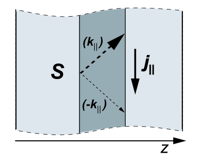
The physics of the tunneling spin-galvanic effect is sketched in Fig.1. We assume two parts of the bulk semiconductor separated by the tunneling barrier grown along direction, and the spin-polarized electron gas on the left side of the structure. Spin-polarized electrons with various wavevectors tunnel through the barrier. In the absence of spin-orbit interaction the barrier transparency reaches maximum for the carriers propagating along the normal to the barrier. Spin-orbit coupling changes this rule, the optimum tunneling transmission is reached now for an oblique incidence. The barrier transparency for the spin-polarized carriers with the certain in-plane wavevector is large than the transparency for the particles with the opposite in-plane wavevector, . This asymmetry results in the in-plane flow of the transmitted electrons near the barrier, i.e. in the interface electric current.
Generally, the barrier transparency depends on the spin orientation of carriers if the system lacks a center of inversion. Two microscopic mechanisms were shown to be responsible for the effect of spin-dependent tunneling. One of them is the Rashba spin-orbit coupling induced by the barrier asymmetry Interface ; Zakharova ; Silva ; Voskoboynikov ; Ting ; Koga . The other is the Dresselhaus spin splitting of the electron states in the barrier grown of a non-centrosymmetrical material such as zinc-blende-lattice semiconductors bulk ; Botha ; Hall . Both these mechanisms lead to the generation of the interface current when the spin-polarized electrons tunnel through the barrier. In the present article we consider the tunneling spin-galvanic effect due to the Dresselhaus splitting as an example.
The theory of the tunneling spin-galvanic effect is developed by using the spin density matrix technique. The interface current of spin-polarized electrons transmitted through the barrier is given by
| (1) |
where is the electron charge, is the momentum relaxation time, is the velocity linked to the electron wavevector by the conventional expression, , is the effective electron mass outside the barrier, and is the spin matrix which describes the flux of the electrons transmitted through the barrier. If the reverse tunneling flux from the right to the left side of the structure is neglected then the matrix is determined by the electron distribution on the left side of the barrier and the spin-dependent coefficient of transmission, and given by
| (2) |
Here is the electron density matrix on the left side of the structure, is the spin matrix of the tunneling transmission linking the incident spinor wavefunction to the transmitted spinor wavefunction , , and -function describes the direction of the tunneling.
We assume the carriers on the left side of the structure to form 3D spin-oriented electron gas, and electron distributions in both spin subband to be thermalized. Thus the density matrix has the form
| (3) |
where is the unit vector directed along the spin orientation, and are the distribution functions of the electrons with the spins oriented parallel and antiparallel to , respectively, and are the Pauli matrices. For the case of small degree of spin polarization, the density matrix of 3D electron gas is simplified to
| (4) |
where is the equilibrium distribution function of non-polarized carriers, is the degree of the spin polarization, and is the average value of the reciprocal kinetic energy of the carriers. The latter is equal to for 3D degenerate electron gas with the Fermi energy , and and 3D non-degenerate gas at the temperature .

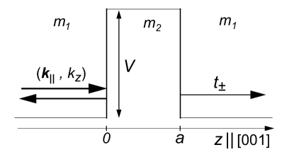
We consider the tunneling spin-galvanic effect for the symmetrical barrier grown of a zinc-blende-lattice semiconductor along direction (see Fig.2). In this case the barrier transparency depends on the orientation of electron spin due to the Dresselhaus spin-orbit interaction. The coefficients of transmission for spin states ”” and ”” corresponding to the most and the less probable tunneling have the form bulk
| (5) |
where is the transmission coefficient when the spin-orbit interaction is neglected, is a constant of the Dresselhaus spin-orbit coupling depending on the material, is the electron effective mass inside the barrier, is the reciprocal length of the wavefunction decay in the barrier, and are the height and the width of the barrier, respectively. The orientations of the electron spin of the states ”” and ”” depend on the direction of the electron in-plane wavevector with respect to the crystal cubic axes. The spinors corresponding to the spin eigen-states are given by bulk
| (6) |
where is the polar angle of the wavevector in the plane, being , and the coordinate system , , and is assumed.
The spin matrix of the electron transmission through the barrier is given by
| (7) |
For our case it has the form
| (8) |
We assume spin corrections to be small, and the coefficient , for simplicity, to depend only on the -component of the electron wavevector. Then substituting the density matrix (4) and the transmission matrix (8) into the expressions (1,2), the interface spin-dependent current is derived to be
| (9) |
where is the flux of the electrons through the barrier, .
The direction of the spin-dependent interface current (9) induced by the Dresselhaus term is determined by the spin orientation of the electrons with respect to the crystal axes. In particular, the current is parallel (or antiparallel) to the spin polarization , if is directed along a cubic crystal axis or ; and is perpendicular to , if the latter is directed along the the axis or .
As it was mentioned above, the tunneling spin-galvanic effect can also be induced by Rashba spin-orbit coupling in asymmetrical barriers. In this particular case the spin-dependent interface current flows perpendicular to the spin polarization of the carriers.
The estimations for the tunneling spin-galvanic current (9) give and for barriers based on GaSb and GaAs, respectively, for the structures with the barrier transparency and the momentum scattering time .
In conclusion, it has been demonstrated that the spin-dependent interface current is generated if spin-polarized carriers tunnel through the semiconductor barrier. The theory of the tunneling spin-galvanic effect has been developed for symmetrical barriers grown of zinc-blende-lattice compounds. The effect could be employed for creating non-magnetic semiconductor detectors of spin-polarized carriers.
This work was supported by the RFBR, the INTAS, and programs of the RAS and the Russian Ministry of Industry, Science and Technologies.
References
- (1) Semiconductor Spintronics and Quantum Computation, edited by D.D. Awschalom, D. Loss, and N. Samarth, Nanoscience and Technology (Springer, Berlin, 2002).
- (2) Optical Orientation, edited by F. Meier and B.P. Zakharchenya (Elsevier Science, Amsterdam, 1984).
- (3) S. Kreuzer, J. Moser, W. Wegscheider, D. Weiss, M. Blicher, and D. Schuh, Appl. Phys. Lett. 80, 4582 (2002).
- (4) P. Van Dorpe, V.F. Motsnyi, M. Nijboer, E. Goovaerts, V.I. Safarov, J. Das, W. Van Roy, G. Borghs, and J. De Boeck, Jap. J. Appl. Phys. 42, L502 (2003).
- (5) R. Fiederling, P. Grabs, W. Ossau, G. Schmidt, and L.W. Molenkamp, Appl. Phys. Lett. 82, 2160 (2003).
- (6) X. Jiang, R. Wang, S. van Dijken, R. Shelby, R. Macfarlane, G.S. Solomon, J. Harris, and S.S.P. Parkin, Phys. Rev. Lett. 90, 256603 (2003).
- (7) M.I. D’yakonov and V.I. Perel’, Phys. Lett. A 35, 459 (1971).
- (8) V.N. Abakumov and I.N. Yassievich, Zh. Eksp. Teor. Fiz. 61, 2517 (1972) [Sov. Phys. JETP 34, 1375 (1972)].
- (9) N.S. Averkiev and M.I. D’yakonov, Fiz. Tech. Poluprovod. 17, 629 (1983) [Sov. Phys. Semicond. 17, 393 (1983)].
- (10) A.A. Bakun, B.P. Zakharchenya, A.A. Rogachev, M.N. Tkachuk, and V.G. Fleisher, Pis’ma Zh. Eksp. Teor. Fiz. 40, 464 (1984) [Sov. Phys. JETP 40, 1293 (1984)].
- (11) E.L. Ivchenko, Yu.B. Lyanda-Geller and G.E. Pikus, Zh. Eksp. Teor. Fiz. 98, 989 (1990) [Sov. Phys. JETP 71, 550 (1990)].
- (12) S.D. Ganichev, E.L. Ivchenko, V.V. Bel’kov, S.A. Tarasenko, M. Sollinger, D. Weiss, W. Wegscheider, and W. Prettl, Nature 417, 153 (2002).
- (13) S.D. Ganichev, Petra Schneider, V.V. Bel’kov, E.L. Ivchenko, S.A. Tarasenko, W. Wegscheider, D. Weiss, D. Schuh, B.N. Murdin, P.J. Phillips, C.R. Pidgeon, D.G. Clarke, M. Merrick, P. Murzyn, E.V. Beregulin, and W. Prettl, Phys. Rev. B68, 081302 (2003).
- (14) A. Voskoboynikov, S.S. Liu, and C.P. Lee, Phys. Rev. B58, 15397 (1998).
- (15) V.I. Perel’, S.A. Tarasenko, I.N. Yassievich, S.D. Ganichev, V.V. Bel’kov, and W. Prettl, Phys. Rev. B67, 201304 (2003).
- (16) A. Zakharova, F.T. Vasko, and V. Ryzhii, J.Phys.: Condens. Matter 6, 7537 (1994).
- (17) E.A. de Andrada e Silva, G.C. La Rocca, Phys. Rev. B59, 15583 (1999).
- (18) A. Voskoboynikov, S.S. Liu, C.P. Lee, and O. Tretyak, J. Appl. Phys. 87, 387 (2000).
- (19) D.Z.-Y. Ting and X. Cartoixa, Appl. Phys. Lett. 81, 4198 (2002).
- (20) T. Koga, J. Nitta, H. Takayanagi, and S. Datta, Phys. Rev. Lett. 88, 126601 (2002).
- (21) A.E. Botha and M.R. Singh, Phys. Rev. B67, 195334 (2003).
- (22) K.C. Hall, W.H. Lau, K. Gundogdu, M.E. Flatte, T.F. Boggess, cond-mat/0307687, Appl. Phys. Lett. , to be published.