Remote-doping scattering and the local field corrections in the 2D electron system in a modulation-doped Si/SiGe quantum well
Abstract
The small, about 30% magnetoresistance at the onset of full spin polarization in the 2D electron system in a modulation-doped Si/SiGe quantum well gives evidence that it is the remote doping that determines the transport scattering time. Measurements of the mobility in this strongly-interacting electron system with remote-doping scattering allow us to arrive at a conclusion that the Hubbard form underestimates the local field corrections by about a factor of 2.
pacs:
73.43.-f, 72.20.-i, 72.20.EeMuch interest has been attracted recently by the behavior of two-dimensional (2D) electron systems in a parallel magnetic field. The resistance of a 2D electron system in Si MOSFETs was found to rise with parallel field saturating to a constant value above a critical magnetic field sat which corresponds to the onset of full spin polarization of the electron system okvit . The spin origin of the effect is consistent with its insensitivity to the direction of the in-plane field sat . At low electron densities, the experimental resistance ratio is equal to as long as the system remains metallic remark , which is in agreement with the calculation dol . The effect was used to study the spin susceptibility of the least-disordered electron system sh as well as the local moments in the bandtail in more-disordered Si MOSFETs pud ; broto . In contrast, the 2D carrier system in GaAs/AlGaAs heterostructures is relatively thick so that the orbital effects become important and give rise to an enhancement of the effective mass in parallel magnetic fields zhu ; tutuc . As a result, in GaAs there are two noteworthy distinctions simmons : (i) above , the resistance keeps on increasing less steeply with no sign of saturation; and (ii) the magnetoresistance is strongly anisotropic depending upon the relative orientation of the in-plane magnetic field and the current.
The 2D carrier systems in Si MOSFETs and high-mobility GaAs/AlGaAs heterostructures are similar in that at low carrier densities, the transport scattering time is determined by charged impurities near the 2D system. In the former system charged impurities are located at the Si/SiO2 interface resulting in dominant large-angle scattering ando , whereas in the latter they are homogeneous background doping for both 2D electrons apl and 2D holes prosk . The case of a 2D carrier system with a finite spacer that is remarkable by remote-doping scattering, i.e., dominant small-angle scattering, is opposite. Although it may seem simple to realize such a 2D system, that kind of scattering has not been unequivocally established in any 2D system studied so far. Recently, it has been predicted that for remote doping, the above resistance ratio should be equal to gold .
In this paper, we report measurements of the resistance of the 2D electron system in a modulation-doped Si/SiGe quantum well in parallel magnetic fields. Being very similar to (100)-Si MOSFETs, this electron system is different by the presence of a spacer and the 1.5 times larger dielectric constant so that the same strength of electron-electron interactions in Si/SiGe can be expected at 2.2 times lower electron densities. The fact that the observed magnetoresistance is small shows that the transport scattering time in our samples is determined by remote doping. In this regime, the magnetoresistance is sensitive to a small amount of the charged residual impurities at the Si/SiGe interface (% of the electron density), which varies in different runs depending on external perturbations such as cooling and illumination of the sample. Using the dependence of the mobility on electron density in this strongly-interacting system with remote-doping scattering, we extract the form of the local field corrections (LFC). From comparison of the experimental data and the model calculations it follows that account should be taken of both kinematic and dynamic correlations.
Samples were grown by molecular beam epitaxy on (001)-Si substrates. A 15 nm thick Si channel was deposited on a strain-relaxed buffer layer which consists of a 600 nm Si0.7Ge0.3 buffer on the top of a 2.5 m thick Si1-xGex layer with compositional grading. The channel was capped by 14 nm Si0.7Ge0.3 spacer, 12 nm P-doped layer, and 27.5 nm cap layer, covered by 10 nm of Si. The samples were arranged in a standard Hall bar geometry. The channel of the transistor had a uniform width of 20 m between the ohmic source and drain contacts. The four voltage probes and the source/drain electrode were formed by local implantation of phosphorous ions. Subsequent activation and recrystallization was performed at 560∘ C for 30 min in an N2 ambient. Afterwards the contact pads were metallized with 25 nm Ti and 100 nm Au. In order to reduce the contact resistance, the sample was annealed at 400∘ C for 60 s in an N2 atmosphere. Finally, the Schottky gate electrode comprising 30/100 nm Ni/Au was defined by a lift off process.
The sample was placed in the mixing chamber of a dilution refrigerator with a base temperature of 30 mK. To create the mobile carriers in the 2D system, the sample was illuminated with a light-emitting diode until the resistance saturated. After the diode was switched off, the sample state did not change in the run. The resistance was measured using a standard four-terminal lock-in technique at a frequency of 15 Hz in magnetic fields up to 14 T. Excitation current through the device was kept low enough ( nA) to ensure that measurements were taken in the linear regime of response. To change the sample position in the mixing chamber we warmed the sample up, rotated it at room temperature, and cooled down again. The alignment uncertainty of the sample plane with the magnetic field was kept within . The electron density as a function of gate voltage was determined from Shubnikov-de Haas oscillations in perpendicular magnetic fields. We have verified that the gate voltage dependence of the resistance in zero magnetic field is well reproducible in different runs with the accuracy of insignificant threshold shifts. In parallel magnetic fields, this dependence was used for determining the threshold voltage.
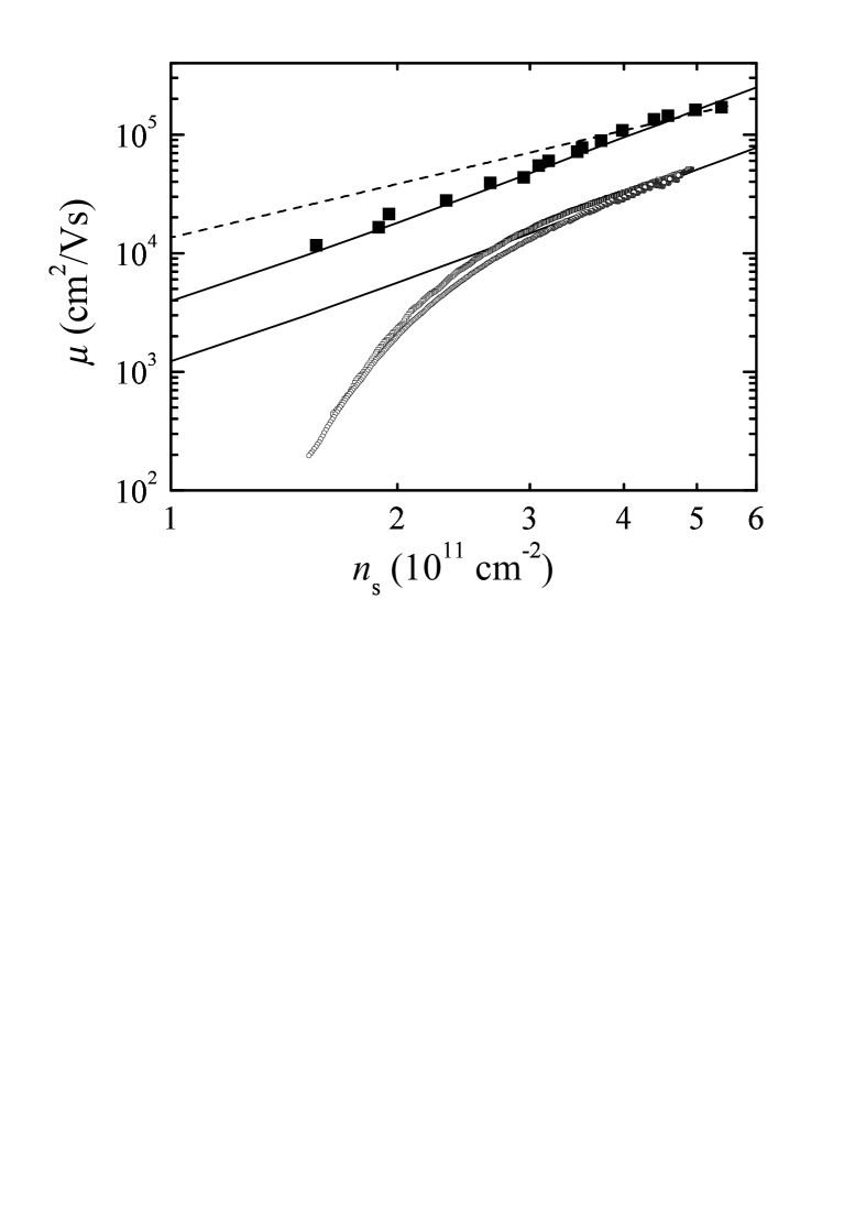
In Fig. 1, we show the dependence of the zero-field mobility, , on electron density, , for two of our samples along with the data of Ref. wil obtained on a Si/SiGe quantum well with higher mobility. We have verified that in the studied range of electron densities, the mobility is temperature-independent below 1 K. Despite the difference between the mobilities is quite appreciable, the slopes of all dependences above cm-2 are coincident and correspond to a power law: , as was observed previously wil ; rem1 . Below cm-2, the stronger decrease of the mobility with lowering electron density in our samples is likely to be a precursor of Anderson localization as caused by multiple scattering agold .
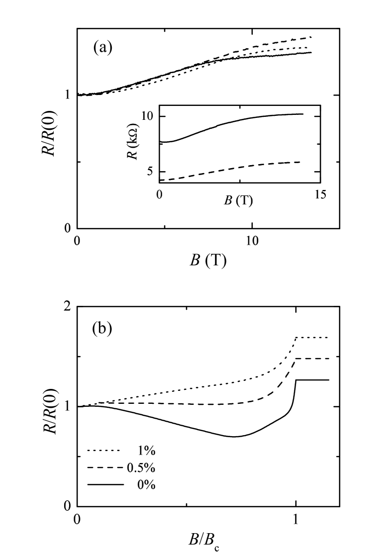
In Fig. 2(a), we show the magnetoresistance of the sample in parallel fields. As the magnetic field is increased, the resistance increases and tends to saturate at the onset of full spin polarization in this electron system. The magnetoresistance is practically independent of the relative orientation of the field and the current, . In other words, no anisotropy of the resistance with respect to the in-plane field is observed in our samples, which is similar to the case of Si MOSFETs. However, as compared to Si MOSFETs, the ratio in the studied range of electron densities is much smaller, about 1.3 rem . This indicates directly that the remote-doping scattering prevails gold . The form of the curve varies slightly in different runs. Even in the same run, it changes slightly with changing electron density (inset to Fig. 2).
We now discuss the regime of remote-doping scattering. The screening properties of a 2D electron system are determined by two parameters: the screening wavevector, , and the Fermi wavevector, (where is the valley degeneracy, is the band mass, and is the dielectric constant). For our case the former equal to cm-1 exceeds the latter which falls within the range cm cm-1 corresponding to the Wigner-Seitz radius . The third parameter that controls the electron scattering in Si/SiGe is half the inverse spacer width, , which is equal to cm-1 in our samples. As in the high- limit the transferred wavevector is small compared to , the electron backscattering is small. In the opposite limit the transferred wavevector is approximately equal to and, therefore, the electron backscattering should occur. Nevertheless, we argue that this is still dominant small-angle scattering. Indeed, in the lowest order of multiple scattering theory gotze the inverse transport scattering time for the two-valley case can be written
| (1) |
where is the LFC and in the case of remote doping is given by
| (2) |
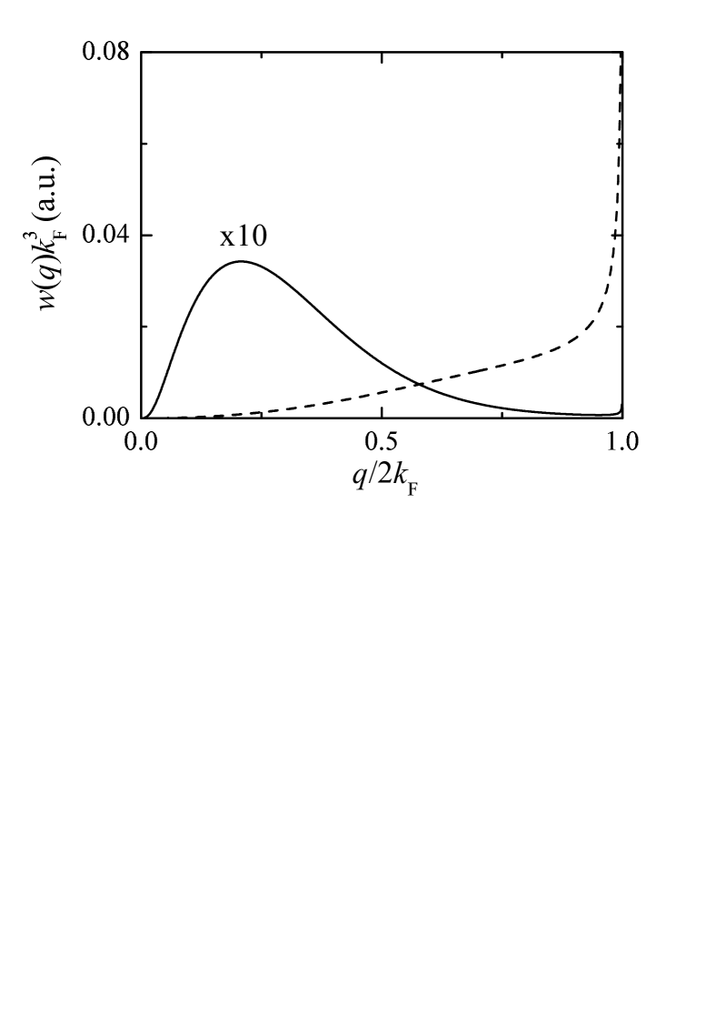
Here is the width of the doped layer with doping density . The dependence of the integrand, , in Eq. (1) on transferred wavevector at high and low electron densities is displayed in Fig. 3 ignoring the LFC. In both limits the main contribution to the scattering probability originates from wavevectors well below , in contrast to Si MOSFETs where the close vicinity of contributes only.
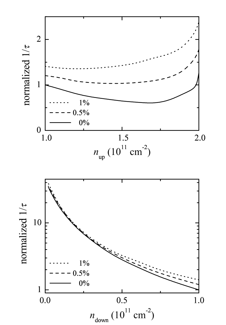
It is remarkable that in the regime of remote-doping scattering, the magnetoresistance at the onset of complete spin polarization is small gold . A qualitative account of this effect is given below. Assuming that the spin flip processes are absent, the calculated scattering rate for spin-up and spin-down electrons as a function of corresponding electron density is shown in Fig. 4. With increasing (or ) the scattering angle decreases and, therefore, the scattering rate decreases except at the onset of complete spin polarization at which the increase of the scattering rate is related to the change of screening, similar to the effect discussed in Ref. dol . The resulting magnetoresistance is negative and only becomes positive near , the ratio being equal to 1.25, see Fig. 2(b). It is important that if there is a small amount of charged impurities at the Si/SiGe interface, the negative magnetoresistance is suppressed accompanied by somewhat larger . The calculated magnetoresistance with 0.5% of the charged impurities (about cm-2) located at the interface describes the experiment reasonably well, see Fig. 2. So, density variations of the charged residual impurities at the Si/SiGe interface and, hence, of the local moments in the bandtail pud naturally explain the observed changes in including those in different runs.
If the local field corrections are still disregarded, the solution to Eq. (1) is agold as shown by the dashed line in Fig. 1. This dependence is noticeably weaker than the experimental one. The origin for the discrepancy is strong correlations in this electron system. At low electron densities, worse screening is reflected by LFC so that the integrand in Eq. (1) should be larger at wavevectors about . The Hubbard form of the LFC
| (3) |
yields a power law , the exponent being still smaller compared to the experimental finding. This is not very surprising because the Hubbard form includes only kinematic correlations that are caused by Pauli principle. Another contribution is given by dynamic correlations that are related to direct Coulomb interelectron interactions; these contribute to the LFC at large wavevectors davoudi . To simulate the effect of dynamic correlations, we demand in Eq. (3). The so-obtained dependence is indicated by the solid lines in Fig. 1 disregarding the numerical factor. Agreement between the calculation and the experiment shows that the LFC are approximately twice as large as the Hubbard form.
Finally, we discuss the above assumption of the absence of spin flip processes. Available experimental data for Si MOSFETs allows one to conclude that such processes are in fact present but are not dominant. Indeed, the Hall resistance in a magnetic field with weak perpendicular and strong parallel components was found to be significantly lower than that expected for decoupled spin subbands vitk . At the same time, ratios were observed at low electron densities in the metallic regime sat ; these are close to the ratio expected for the case when no spin flip occurs, whereas twice as low a ratio is expected if the spin flip time is the shortest dol . This gives evidence that the spin flip processes are not of importance and, thus, the above considerations are justified.
In summary, we have established that in the 2D electron system in a modulation-doped Si/SiGe quantum well, the regime of remote-doping scattering occurs in which the parallel-field magnetoresistance is small and sensitive to uncontrollable density variations of the charged residual impurities at the Si/SiGe interface. Based on analysis of the mobility as a function of electron density in this regime, we conclude that the local field corrections are approximately double the Hubbard form and, therefore, both kinematic and dynamic correlations make significant contribution.
We gratefully acknowledge discussions with A. Gold, V. S. Khrapai, and S. V. Kravchenko. We would also like to thank D. Scheible, C. Meyer, and S. Manus for technical help. This work was supported by A. von Humboldt Foundation via Forschungspreis, the Russian Foundation for Basic Research, and the Russian Ministry of Sciences.
References
- (1) V. T. Dolgopolov, G. V. Kravchenko, A. A. Shashkin, and S. V. Kravchenko, JETP Lett. 55, 733 (1992); D. Simonian, S. V. Kravchenko, M. P. Sarachik, and V. M. Pudalov, Phys. Rev. Lett. 79, 2304 (1997); S. V. Kravchenko, D. Simonian, M. P. Sarachik, A. D. Kent, and V. M. Pudalov, Phys. Rev. B 58, 3553 (1998); K. M. Mertes, D. Simonian, M. P. Sarachik, S. V. Kravchenko, and T. M. Klapwijk, Phys. Rev. B 60, R5093 (1999); V. M. Pudalov, G. Brunthaler, A. Prinz, and G. Bauer, JETP Lett. 65, 887 (1997); A. A. Shashkin, S. V. Kravchenko, and T. M. Klapwijk, Phys. Rev. Lett. 87, 266402 (2001).
- (2) T. Okamoto, K. Hosoya, S. Kawaji, and A. Yagi, Phys. Rev. Lett. 82, 3875 (1999); S. A. Vitkalov, H. Zheng, K. M. Mertes, M. P. Sarachik, and T. M. Klapwijk, Phys. Rev. Lett. 85, 2164 (2000).
- (3) At electron densities below approximately (where is the density for the zero-field metal-insulator transition), the application of a strong parallel magnetic field makes the system insulating, in which case the ratio may become arbitrarily high sat .
- (4) V. T. Dolgopolov and A. Gold, JETP Lett. 71, 27 (2000).
- (5) A. A. Shashkin, S. V. Kravchenko, V. T. Dolgopolov, and T. M. Klapwijk, Phys. Rev. Lett. 87, 086801 (2001); S. V. Kravchenko, A. A. Shashkin, and V. T. Dolgopolov, Phys. Rev. Lett. 89, 219701 (2002).
- (6) V. M. Pudalov, G. Brunthaler, A. Prinz, and G. Bauer, Phys. Rev. Lett. 88, 076401 (2002); V. T. Dolgopolov and A. Gold, Phys. Rev. Lett. 89, 129701 (2002); A. Gold and V. T. Dolgopolov, J. Phys. Condens. Matter 14, 7091 (2002).
- (7) J. M. Broto, M. Goiran, H. Rakoto, A. Gold, and V. T. Dolgopolov, Phys. Rev. B 67, 161304(R) (2003).
- (8) J. Zhu, H. L. Stormer, L. N. Pfeiffer, K. W. Baldwin, and K. W. West, Phys. Rev. Lett. 90, 056805 (2003).
- (9) E. Tutuc, S. Melinte, E. P. De Poortere, M. Shayegan, and R. Winkler, Phys. Rev. B 67, 241309 (2003).
- (10) M. Y. Simmons, A. R. Hamilton, M. Pepper, E. H. Linfield, P. D. Rose, D. A. Ritchie, A. K. Savchenko, and T. G. Griffiths, Phys. Rev. Lett. 80, 1292 (1998); J. Yoon, C. C. Li, D. Shahar, D. C. Tsui, and M. Shayegan, Phys. Rev. Lett. 84, 4421 (2000); S. J. Papadakis, E. P. De Poortere, M. Shayegan, and R. Winkler, Phys. Rev. Lett. 84, 5592 (2000).
- (11) T. Ando, A. B. Fowler, and F. Stern, Rev. Mod. Phys. 54, 473 (1982).
- (12) A. Gold, Appl. Phys. Lett. 54, 2101 (1989).
- (13) Y. Y. Proskuryakov, A. K. Savchenko, S. S. Safonov, L. Li, M. Pepper, M. Y. Simmons, D. A. Ritchie, E. H. Linfield, and Z. D. Kvon, J. Phys. A: Math. Gen. 36, 9249 (2003).
- (14) A. Gold, Physica E 17, 305 (2003).
- (15) Z. Wilamowski, N. Sanderfeld, W. Janish, D. Toebben, and F. Schaeffler, Phys. Rev. Lett. 87, 026401 (2001).
- (16) An attempt to account for the strong dependence was made in Ref. wil based on the idea of worse screening of potential fluctuations with lowering due to a decrease of the average thermodynamic density of states near the metal-insulator transition. However, as the range of potential fluctuations found in that paper exceeds the electron mean free path, the scattering calculations using the average thermodynamic density of states in such an inhomogeneous electron system are obviously incorrect.
- (17) A. Gold, Phys. Rev. B 44, 8818 (1991).
- (18) A similar dependence was observed by T. Okamoto, M. Ooya, K. Hosoya, and S. Kawaji, cond-mat/0307521.
- (19) A. Gold and W. Gotze, Phys. Rev. B 33, 2495 (1986).
- (20) B. Davoudi, M. Polini, G. F. Guliani, and M. P. Tosi, Phys. Rev. B 64, 153101 (2001).
- (21) S. A. Vitkalov, Phys. Rev. B 64, 195336 (2001).