Condition of the occurrence of phase slip centers in superconducting nanowires under applied current or voltage
Abstract
Experimental results on the phase slip process in superconducting lead nanowires are presented under two different experimental conditions: constant applied current or constant voltage. Based on these experiments we established a simple model which gives us the condition of the appearance of phase slip centers in a quasi-one-dimensional wire. It turns out that the competition between two relaxations times (relaxation time of the absolute value of the order parameter and relaxation time of the phase of the order parameter in the phase slip center ) governs the phase slip process. Phase slip phenomena, as periodic oscillations in time of the order parameter, is possible only if the gradient of the phase grows faster than the value of the order parameter in the phase slip center, or equivalently if .
pacs:
74.25.Op, 74.20.De, 73.23.-bI Introduction
Since the discovery of superconductivity it was expected that if the superconductor was subjected to a constant electric field superconductivity will inevitably be destroyed. The reason is that the superconducting electrons will be accelerated by the electric field and will reach a velocity above its critical velocity. However if the sample is short enough or if the electric field exists only in a small part of the sample such that the path over which the Cooper pairs are accelerated are sufficiently short an electric field can exist in the sample in the presence of superconductivity. Another example is the presence of an electric field in the superconducting sample which is attached to a normal metal. In this geometry the injected current from the normal metal will be converted into a superconducting current on a distance of about the charge imbalance distance () and on that scale an electric field will exist in the sample Tinkham1 . In this case the electric field is compensated by the gradient of the chemical potential of superconducting electrons and it does not lead to an acceleration of the superconducting condensate (see for example the book of Schmidt Schmidt ).
But there is another mechanism which allows superconductivity to survive in the presence of an electric field deep in the superconducting sample of arbitrary length. This is the phase slip mechanism. Initially this phenomena was used in order to estimate the relaxation time of superconducting current in a superconducting wire Langer . If the order parameter vanishes in one point of the wire the phase of the superconducting order parameter exhibits a jump of at that point Langer and as a result the momentum decreases by . So even if the electric field accelerates the superconducting electrons it does not lead to a destruction of supercondictivity because the momentum is able to relax through the phase slip mechanism.
This simple idea was understood already a long time ago. Therefore, it is very surprising that there are practically no experimental nor theoretical works studying in detail what will happen if a voltage (i.e. electric field) is applied to the superconductor. In previous works mainly the situation with applied current (i.e. the I=const regime) was studied. In the latter case the phase slip process was studied theoretically in detail (see for example the review of Ivlev and Kopnin Ivlev and the books of Tinkham Tinkham1 and Tidecks Tidecks ). On the basis of a numerical solution of the extended time-dependent Ginzburg-Landau equations it was found that the phase slip (PS) phenomena exists in some region of currents. The lowest critical current at which a PS solution first appears in the system may be smaller than the depairing Ginzurg-Landau current density and as a result it leads to hysteresis in the I-V characteristics in the I=const regime Ivlev ; Tidecks .
The I=const regime was also studied experimentally in a number of works Ivlev ; Tidecks starting from the paper of Meyer and Minnigerode Meyer1 ; Meyer2 . The most characteristic effect of the phase slip mechanism is the appearance of a stair like structure in the current-voltage characteristics. In Ref. Skocpol a simple phenomenological model was built in order to quantitatively describe this feature. It was proposed that every step in the I-V characteristic is connected with the appearance of a new phase sip center (PSC) that increases the resistivity of the sample by a finite value. In this model, it was conjectured that in a region of the sample with size of about the coherence length fast oscillations of the order parameter occurs in time which produces normal quasi-particles. Because of the finite time needed to convert normal electrons into superconducting electrons Tinkham1 ; Schmidt there is a region of size of about near the phase slip center where the electric field and the normal current are different from zero. It means that the chemical potential of superconducting and normal electrons are different near PSC and their difference is proportional to the charge imbalance Q in a given point of the superconductor Tinkham1 ; Skocpol . Because usually it is possible to neglect the -sized region with oscillating and consider that phenomena as a time-independent process. Such a model gives a finite voltage, which is connected with every phase slip center, which is equal to with the normal resistivity, S the cross-section of the current carrying region, is the critical current and is a phenomenological parameter. In the experiment of Dolan and Jackel Dolan the distribution of and near a PSC were measured which fully supported the idea of Ref. Skocpol that a difference exist between and near the phase slip center.
Despite numerous theoretical and experimental works the physical conditions under which phase slip phenomena can exist is still not clear. In a review Ivlev on this subject it was claimed that phase slip phenomena are connected with the presence of a limiting cycle in the system which leads to such type of oscillations. But it was not explained how and why it leads to the phase slip phenomena.
Based on our previous work Vodolazov2 on the time-dependent Ginzburg-Landau equations (the investigated systems were superconducting rings in the presence of an external magnetic field) we know that systems which are governed by such equations exhibit two relaxation times. One is the relaxation time of the phase of the order parameter and the other is the relaxation time of the absolute value of the order parameter . In Ref. Vodolazov2 it was established that phase slip processes can occur in such systems when roughly speaking . In the present paper we discuss this question in the context of superconducting wires in the presence of an applied current or voltage.
To our knowledge there exists only a single theoretical work in which a superconducting wire in the presence of an applied voltage was studied Malomed . The authors used the simple time-dependent Ginzburg-Landau equations and found that the behavior of the system is very complicated and strongly depends on the length of the wire and the applied voltage. Neither a detailed analysis nor any physical interpretation of their results was presented. In a recent letter Vodolazov1 we presented our preliminary theoretical and experimental results on the dynamics of the superconducting condensate in wires under an applied voltage. It turned out that in this case the I-V characteristics exhibit a S-shape which was explained by the appearance of phase slip centers in the wire and their rearrangement in time. In the present paper we will present more details and extend our previous work to the situation in which defects are present, and we investigate the effects of boundary conditions and an applied magnetic field.
The paper is organized as following. In Sec. II we present our theoretical results and give the conditions for the existence of phase slip centers when current (Sec. IIa) or voltage (Sec. IIb) is applied to the superconducting wire. In Sec. III we show our experimental results and in Sec. IV we compare theory and experiment.
II Theory
We study the current-voltage characteristics of quasi-one-dimensional superconductors using the generalized time-dependent Ginzburg-Landau (TDGL) equation. The latter was first written down in the work of Ref. Kramer1
| (1) |
In comparison with the simple time-dependent Ginzburg-Landau equation where it allows us to describe a wider current region (with a proper choice of the parameters and ) where a superconducting resistive state exists and gives us a wider temperature region in which Eq. (1) is applicable Kramer1 ; Kramer2 ; Watts-Tobin . The inelastic collision time for electron-phonon scattering is taking into account in the above equation through the temperature dependent parameter ( is the equilibrium value of the order parameter).
Eq. (1) should be supplemented with the equation for the electrostatic potential
| (2) |
which is nothing else than the condition for the conservation of the total current in the wire, i.e. . In Eqs. (1,2) all the physical quantities (order parameter , vector potential and electrostatical potential ) are measured in dimensionless units: the vector potential and momentum of superconducting condensate is scaled by the unit (where is the quantum of magnetic flux), the order parameter is in units of and the coordinates are in units of the coherence length . In these units the magnetic field is scaled by and the current density by . Time is scaled in units of the Ginzburg-Landau relaxation time , the electrostatic potential (), is in units of ( is the normal-state conductivity). In our calculations we mainly made use of the bridge geometry boundary conditions: , , and . We chose these boundary conditions because at low temperatures the normal current is converted to a superconducting one due to the Andreev reflection on a distance of about near the boundary Tinkham1 ; Hsiang . It means that practically there is no injection of quasi-particles from the normal material to the superconductor and hence we can neglect the effect of charge imbalance near the S-N boundary. The bridge geometry boundary conditions models this situation. The parameter is about according to Ref. Kramer1 . We also put in Eq. (1,2) because we considered the one-dimensional model in which the effect of the self-induced magnetic field is negligible and we assume that no external magnetic field is applied.
II.1 Constant current regime
Lets consider first the more simple case when a constant external current is applied to the sample. In such a case it was theoretically found Kramer1 ; Kramer2 that the system exhibits hysteretic behavior. If one starts from the superconducting state and increases the current the superconducting state switches to the resistive superconducting or normal state at the upper critical current density which, in a defectless sample, is equal to the Ginzburg-Landau depairing current density . Starting from the resistive state and decreasing the current it is possible to keep the sample in the resistive state even for currents up to (which we call the low critical current). For such a state is realized as a periodic oscillation of the order parameter in time at one point of the superconductor Kramer1 ; Kramer2 . When the order parameter reaches zero in this point a phase slip of occurs. This is the reason why such a state is now called a phase slip state and this point a phase slip center (PSC). Using results obtained in our earlier work Vodolazov2 we claim that the value of depends on the ratio between the two characteristic times in the sample: the phase relaxation time of the order parameter and the relaxation time of the absolute value of the order parameter in the region (with size of about ) where the oscillations of the order parameter occurs.
Having written Eq. (1) for the dynamics of the phase and the absolute value of the order parameter in a quasi-one dimensional wire of length L (-L/2sL/2)
| (3a) | |||||
| (3b) | |||||
it is easy to estimate both these times. Indeed, from Eq. (3a) it directly follows that
| (4) |
To determine we need to know how fast the phase changes over the region (with size of about ) at which the order parameter oscillates. Our numerical calculation shows that the time-average of the derivative is (with C(s)=const and the theta function). Because the time-averaged electrostatic potential changes over a distance for (where is the decay length of the normal current density and the charge imbalance ) and that the order parameter is about unity already at , we can estimate this constant as . Consequently we find that
| (5) |
The product is roughly the voltage drop ’produced’ by the phase slip center Skocpol . Thus the time change of the phase of the order parameter in the phase slip center is inversely proportional to the voltage drop over the whole structure (and ). This is a consequence of the fact that the time-averaged electro-chemical potential of the superconducting electrons does not change in space and its jump near the phase slip center is equal to the voltage drop of this structure in the sample. In terms of the language used by Schmid and G. Schön Schmid , is the ’longitudinal’ time and decreases with increasing ’transverse’ time because . In Ref. Vodolazov2 it was found that the phase slip events occur periodically in time when . This gives us an estimation for the lower critical current
| (6) |
By varying the parameter we can change both and and hence we can vary . In Fig. 1 we show the voltage in the sample, the normal current density and the absolute value of the order parameter in the phase slip center averaged over the time as a function of the external current for two different values of . In our simulations we started from the superconducting state with . At the system jumps instantaneous to the resistive state with finite voltage self1 . Than we decrease the external current and at the system transits to the purely superconducting state with . We should emphasize that at the voltage jumps by a finite value (this result is qualitatively different to the results of Ref. Kramer1 ; Watts-Tobin where the authors found that at .). It means that there is a non-infinite maximal oscillation period for the order parameter in the phase slip center. We believe that the finite voltage jump or finite period of oscillations is directly connected with the threshold condition for activation of regular phase slip processes in the constant current regime and it means that .
Before going further we should stress here that the above condition for the existence of a phase slip process is a rather rough estimate. Indeed, Eqs. 3(a,b) are a coupled system of equations, and besides , it explicitly (see Eq. (4)) depends on the value of . However, the above condition allows us to explain the general qualitative properties of the phase slip processes (including the existence of , and its dependence on and ) and predict new features which will be discussed below.
Far enough from the dependence of on the current is close to linear. When the current increases, decreases (see Eq. (5)) and hence the time between two phase slips also decreases and the order parameter has less time for recovering at the phase slip center. That is the reason why the time averaged voltage increases (as ), the averaged order parameter decreases and the fraction of the normal current increases with increasing external current. It is interesting to note that from the phenomenological Skocpol-Beasley-Tinkham (SBT) Skocpol model it follows that which qualitatively resembles the dependence shown in Fig. 1(b).
Let us now discuss the effect of defects on the I-V characteristic. This question was considered previously in Ref. Kramer3 for two different models of defects: local variation of the critical temperature and a local variation of the mean free path. We will repeat these calculations partially and interpret it in terms of a competition between and . In addition to the first type of defect we will also study the effect of the variation of the cross-section of the wire.
The first type of defect is the inclusion of a region in the superconductor which suppresses and the order parameter becomes lower than the equilibrium value even in the absence of any external current. This is modelled Kramer3 by introducing the term in the right hand side (RHS) of Eq. (1). In the present calculation we choose . The larger the more the order parameter is suppressed in the center of the wire. Firstly, such a defect leads to a decrease of the upper critical current . Secondly, it decreases the lower critical current . Indeed, when we introduce a defect, the RHS of Eq. (3a) decreases at the spatial position where the order parameter oscillations and hence needs more time to change in that spatial position. Thus this type of defect leads to an increase of the relaxation time of the order parameter in the region of the defect (as an indirect prove of this we found a decreasing with increasing ’strength’ of the defect). If the size of the defect is smaller than we can neglect its effect on the relaxation time of the phase of the order parameter. Finally, we can conclude that the ’stronger’ the defect the smaller the value of the lower critical current .
In Fig. 2(a) we present our numerical results for two different values of . With increasing ’strength’ of the defect the upper and lower critical currents decrease and start to merge. As a consequence the hysteresis in the I-V characteristics will disappear when the defect is sufficiently strong.
The second type of defect is one for which we have a local decrease of the cross-section of the wire. In this case we expect that will not be influenced. The situation with is more complicated because a large part of the superconductor with size of about participates in the formation of this time. Two limiting cases can be distinguished. If the defect is much smaller than we can neglect its effect on and hence we will have the same lower critical current as for the case of an ideal wire. In the opposite case of a defect with size much larger than we only have to take into account the increased current density in the part of the wire where we have a smaller cross-section and apply Eq. (5). In this case the current is decreased by a factor , where is the average cross-section and is the local reduced cross-section.
Another important question is the value of the upper critical current . If the size of the defect is larger than then the proximity effect from adjacent parts near the defect will be small and will decrease by a factor (in the opposite case the current is almost defect independent). Therefore, for a defect with length the I-V characteristic may be reversible with a proper choice of the parameters (like in the case of a local suppression of ). In Fig. 2(b) we show the results of our numerical calculations and we obtain a qualitative agreement with the above physical arguments. When the length of the defect is smaller than then the lowest critical current density practically does not change. In the opposite case decreases by a factor of . The upper critical current density changes considerably only if the length of the defect exceeds . Unfortunately, we are not able to consider the case for which the length of the defect is simultaneously much smaller than and much larger than because of computational restrictions. For example, when we increase by a factor of two the time of calculations increases also by a factor of two but the ratio increases roughly only by a factor of for . The reason is that when we increase we need to take a smaller time step (see Eq. (1)) which increases the computation time.
When the wire has a length less than then this will affect the distribution of the normal current density in the wire and hence the time and the lower critical current . Indeed from our bridge boundary conditions it follows that (see Eq. 3(b)). Then taking into account that we can easily obtain, in the limit , that
| (7) |
where the current is the average normal current in the phase slip center.
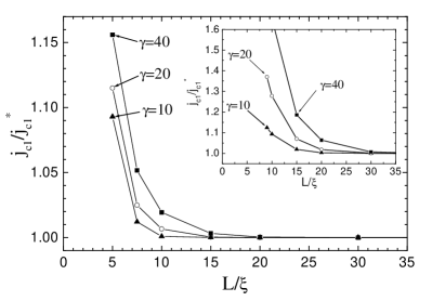
The voltage jump at should not change with varying (at least for when proximity effect does not have an effect on ). From Eq. (7) it follows then that the normal current density increases with increasing length. But should always be smaller than the full current . It implies that the critical current density will increase with increasing length of the wire as in order to keep the ratio constant. Fig. 3 illustrates the dependence of on the length of the wire which we obtained on the basis of a numerical solution of Eqs. (1,2). Unfortunately, in our calculations we are not able to use very large values of and the maximal value of was for . But nevertheless, we found that increases with decreasing wire length. We should add here that we also found that also decreases a little bit. We connect it with a small change in due to the small length of the wire and hence the increased effect of the boundaries.
The more pronounced effect of the finite length of the wire on the value of is found for the case that we used N-S boundary conditions: and . These boundary conditions are approximately valid for samples at temperatures close to . It is easy to show that in this case
| (8) |
where (see Fig. 1(b)). In this case also increases with decreasing wire length (see inset in Fig. 3). But besides there is a finite length for which . It implies that the phase slip process is not possible in wires with length . In such wires the system goes from the superconducting state directly to the normal state.
Not only the finite length of the sample is able to change the value of . If we apply a magnetic field parallel to the length of the wire it will suppress the order parameter in the sample. Our analysis shows that if the diameter of the wire is less than and if we can neglect screening effects () then the distribution of the order parameter will be uniform along the cross-section of the wire. The order parameter depends on H as
with . This behavior is very similar to the behavior of a thin plate in a parallel magnetic field Ginzburg ; Douglass or a thin and narrow ring in a perpendicular magnetic field Vodolazov3 . In all cases the transition to the normal state is of second order and the vorticity in the wire will be equal to zero due to the small cross-section of the sample.
Because the order parameter practically does not depend on the radial coordinate of the wire we can use the one-dimensional model in order to study the response of the system on the applied current. In order to take into account the suppression of by magnetic field () we add to the RHS of Eq. (1) the term . In some respect it is similar to the way we introduced the first type of defect in our wire. We can expect that will increase with increasing (because the ’strength’ of the ’defect’ increases). But because the magnetic field suppresses the order parameter everywhere in the sample it also leads to an increase of , because in the TDGL model . It is clear that both these processes should decrease . The strongest mechanism is connected with the change in . Indeed it is easy to estimate that and . Even if we take into account that the parameter may decrease with increasing H (because in non-zero magnetic field there is another pair-breaking mechanism and instead of we should useSchmid ; Kadin1 with ) it does not lead to an increase of with an increase of because changes faster than even in this case.
In the above model it is easy to show that for the case of an uniform wire. In Fig. 4 we present the results of our numerical calculations. We found that both and decreases with increasing magnetic field and at some they practically merge. Unfortunately, it is quite difficult to find an analytical expression for the dependence of like we had for . The reason is the complicated behavior of the dynamics of in the phase slip center.
The variation with increasing was obtained experimentally in Ref. Kadin1 . To compare with the theory the authors of Ref. Kadin1 used the expressions found in the work of Schmid and Schön Schmid which are valid in the limit . It is interesting that in Ref. Kadin1 it was found that expressions of Schmid and Schön are quantitatively valid even far from . From this observation we may hope that the present theoretical results are also valid over a wider temperature range than only near .
The main conclusion which follows from the change of with decreasing wire length and/or applying magnetic field is that there exist a critical length (or critical field ) below(above) which the current becomes equal to . It implies that for wires with lengths and/or fields there will be no jump in the voltage in the current-voltage characteristic and the I-V curve will be reversible. It will also result in the absence of a S-behavior in the V=const regime (see section below).
II.2 Constant voltage regime
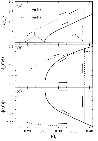
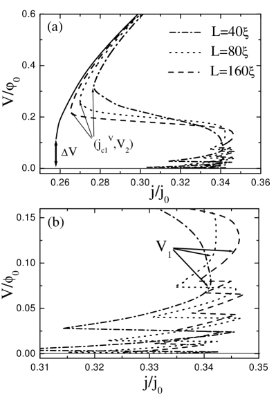
In our earlier work we found that the I-V in the regime exhibits an S-like behavior Vodolazov1 and furthermore for low voltages there is an oscillatory dependence of the current on the applied voltage (see Fig. 5). As was shown in Ref. Vodolazov1 these properties are connected with the existence of two critical currents and . Here, we will discuss the characteristic voltages , (see Fig. 5) and their dependence on the length of the sample.
If we apply a voltage to the wire of length then in the sample an electric field exist which will accelerate the superconducting electrons. When the current density approaches phase slip centers will spontaneously appear in the sample. As a result the momentum of the superconducting electrons (and hence the current) will decrease by after each phase slip event. When the current density decreases below the phase slip process will no longer be active and the applied electric field will be able to accelerate the superconducting condensate. This process leads to periodic oscillations in time of the current in the sample.
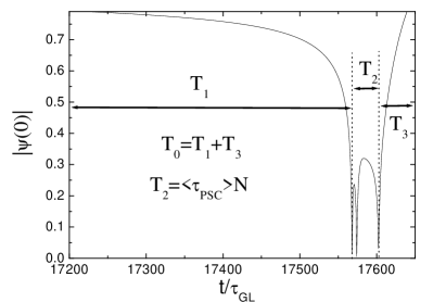
We can divide the period of oscillations (at least at voltages ) in two parts. First, the longest part is the one during which the condensate is accelerated by the electric field till the moment reaches . The second part we call the transition period . The transition period also consists of two parts: the time needed for the phase slip processes (which is proportional to the number of phase slip events and hence the length of the wire) and the time for the decay of the order parameter from (when ) till the first phase slip event and for the recovering of back to from zero after the last phase slip event (see Fig. 6). The minimal number of phase slip events which occur during the transition time is determined by the internal parameters of the superconductor () and its length Vodolazov1 which is given by
| (9) |
where is the smallest real root of the equation and returns the nearest integer value.
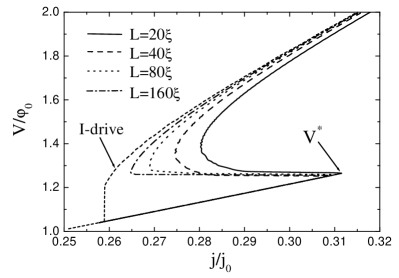
At the time-averaged current increases (with oscillations) and in the range it decreases with increasing voltage. The lowest minimal current in the latter region is which depends on the length of the system (see Fig. 5 and Ref. Vodolazov1 ). In Fig. 7 we present the dependence of the above voltages on the length of the wire. The explanation for their different behavior is the following. At a voltage the period of the oscillation (N is the number of phase slip events during the transition time) of the current becomes of order . The time does not depend on the length and the voltage at . So, we can estimate as
| (10) |
where is the average time between two phase slip events and is the coefficient which depends on (see Eq. (9)) and hence on the specific superconductor. When the voltage becomes practically independent of the length. Because the time depends on the relaxation time of the absolute value of the order parameter the length of the wire at which saturates depends on the internal parameters of the superconductor.
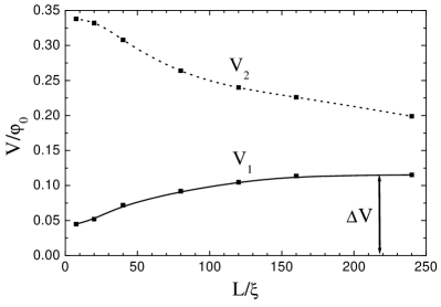
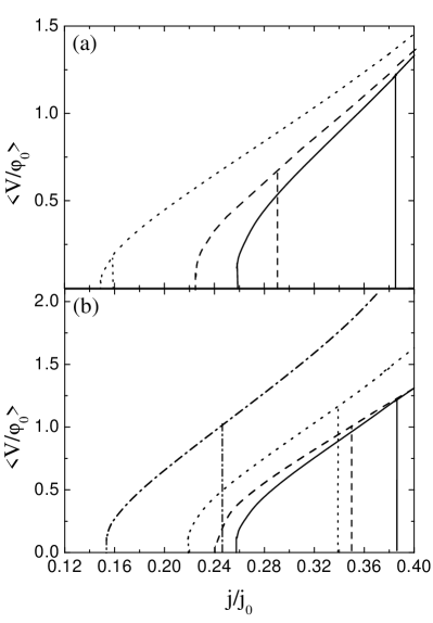
The voltage decreases with increasing length of the sample because the lower critical current decreases. It is interesting to note that with accuracy of finding the saturated value of the lower critical voltage coincides with the voltage jump at in the constant current regime. Because the minimal value of is equal to for an infinitely long wire we may conclude that with increasing wire length the I-V characteristic in the range of voltages approaches the horizontal line.
Defects, magnetic field, short length of the sample etc. will decrease the hysteresis and consequently the currents and approaches each other. If the difference between them will be small enough the S-shape of the I-V characteristic at the constant voltage regime changes to the usual monotonic behavior (see Fig. 8). This happens because when the voltage approaches , the maximal current during the period of the current oscillation will be about (because cannot substantially exceed but is already close to in this case).
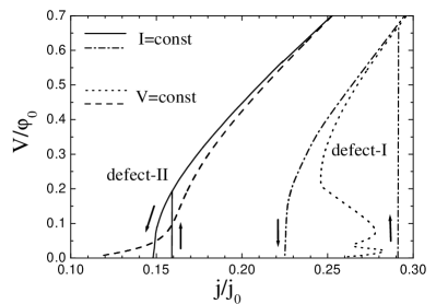
We also would like to discuss how the change of the boundary conditions will change the shape of the I-V characteristic. If we apply the N-S boundary conditions the I-V curve in the voltage driven regime also exhibits an S-behavior but without oscillations in the current at small voltages (see Fig. 9). In this case there will always be an inevitable voltage drop near the boundaries connected with the current in the wire through the relation (because the electric field and the normal current decays on a scale of the charge imbalance length near the boundaries Tinkham1 ). Near the boundary the nonzero electric field is compensated by the term (see Eq. 3(b) - and in our units) and the superconducting electrons are not accelerated by this field. The situation is very similar to the case when we inject a current in the wire. When the current generated by this voltage reaches the phase slip process becomes possible in the system. But like the case of the current driven regime the superconducting state can be stable(metastable) until the current reaches at . From our estimates it follows (see section below) that the fluctuations of the order parameter are very important in our samples. Therefore, in our calculations we introduce at some moment of time (at fixed voltage) a phase slip center in the center of the wire and checked if it will survive or not. As a result we obtained the I-V characteristics as presented in Fig. 9. When the voltage is less than some critical value () the phase slip process decays in time and the resulting current in the wire is time-independent. The whole voltage drop occurs near the boundaries. At (and ) the dynamics of the condensate in the wire will be similar to the case considered above for .
The reason for this is as follows. The current density in the wire at small voltages will always be less than and due to the relation . When the current density reaches the phase slip process becomes possible in the sample. But such a phase slip process leads to a finite voltage. As a consequence the voltage drop at the boundaries will sharply decrease when a phase slip center is created. But it implies that the full current density will also decrease and consequently will become less than . We can conclude that the phase slip process may survive in such a type of superconductor only if the applied voltage will be roughly equal to plus the voltage drop near the boundaries necessary for the creation of a current larger than .
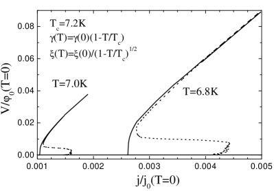
Concluding the theoretical part, we present in Fig. 10 the I-V characteristics in the I=const and V=const regimes at different temperatures close to . With decreasing temperature the range of currents, where there is a S-behavior increases and the voltages and increases. It resembles the experimental results presented in Vodolazov1 ; Michotte and in the subsequent Section III.
III Experiment
| L | d(nm) | Rn(7.1K)() | Rres(4.3K)() | Hc(4.5K)(T) | (4.5K)(nm) | (4.5K)(nm) | (7.1K)( cm) | |
|---|---|---|---|---|---|---|---|---|
| A | 22 | 40 | 300.9 | 14.9 | 1.271 | 37 | 16 | 1.67 |
| B | 50 | 55 | 210.2 | 21.7 | 0.925 | 38 | 19 | 0.86 |
| C | 50 | 55 | 465.9 | 80.7 | 1.652 | 21 | 14 | 1.75 |
| D | 50 | 70 | 94.6 | 17.6 | 0.591 | 46 | 24 | 0.52 |
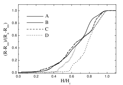
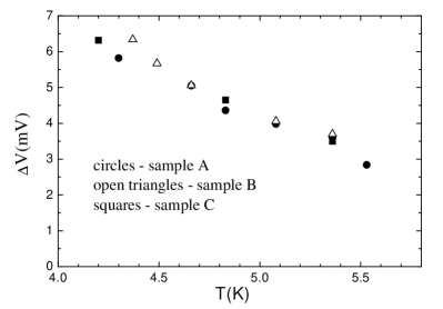
Measurements of the I-V characteristics were done on single Pb nanowires Vodolazov1 ; Michotte with typical diameter about and length (see Table I). At first we would like to discuss the rather wide resistive transitions and strong magneto-resistance effect (see Figs. 11-12) in our samples. We may claim, taking into account the small diameter of our nanowires, that the effect of the thermo-activited Langer and the quantum-activated Giordano ; Tinkham2 phase slip phenomena is very strong in our samples. It is easy to see that with increase of the diameter of the nanowire the width of the resistive transition decreases. Our estimations, based on Giordano expressions, Giordano showed that for sample A even at the number of quantum phase slip events should be about per second. That is the reason why we did not observe in our experiment any hysteresis in the current driven regime (see below). But this rate is not large enough for destroying the S-behavior in the voltage driven regime. Indeed, the period of oscillations of the current for Pb is about s at and . It means that only at temperatures close to the fluctuating PSC’s will interrupt the internal temporal oscillations in the order parameter and ruin the S-behavior. In other words the system can be in a state with only during a time which is less than the time between two phase slips. This results in the coincidence of the I-V characteristics both in the current and the voltage driven regimes at temperatures close to (see Fig. 3 in Ref. Michotte ). We would like also to mention the small difference in the critical temperatures which implies that all our samples have practically the same value of the superconducting gap.
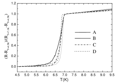
As can be seen in Fig. 12, the wider the transition width in , the smaller the magnetic fields where the resistance starts to increase with increasing magnetic field.
Of course, our nanowires are not free from imperfections. Although our fabrication technique produce samples which are quite regular (see Ref. Michotte for Scanning Electron Microscopy (SEM) picture), we may distinguish two kinds of imperfections. Firstly, there can be deviations from an ideal cylindrical shape. Indeed, although the nanopores of the membrane in which the nanowires are grown are designed to be as regular as possible, there may exist a smooth variation in diameter along the length of the nanowire, which we estimated to be not more than 10 . However, in addition to these smooth variations, it may happen that a defect in the membrane leads to a constriction in the measured nanowire. In this case, the diameter can be locally reduced quite importantly and this results in a lower critical current and a larger critical magnetic field. This is in fact what we observed in sample C. In addition to such shape imperfections, we note also that the parameters of our nanowires strongly vary from sample to sample - see table I (we estimated the coherence length using the expression () and () for the critical field). The reason for this difference in resistivity is related to the second kind of imperfections, which is structural disorder that is formed during the electrodeposition of these nanowires inside the nanopores. Indeed, as shown in Ref. Dubois , these nanowires are polycrystalline and inevitably contain structural defects such as dislocations, twins, etc. These two kinds of imperfections results in differences in the I-V characteristics (Fig. 13). For example for samples A and B we observed two jumps in the voltage which we explain by the appearance of two successive phase slip centers in the nanowire but for sample C we found only one jump in the voltage. Indeed, due to the presence of a constriction in this sample, heating may drastically affect the behavior of this sample, precipitating the return to the normal state. Unfortunately sample D was broken during the measurements and we could not measure its I-V characteristic.
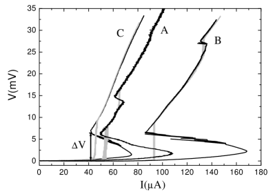
We found that jumps in the voltage are practically the same for all three samples (see Figs. 13-14). It agrees with the theory presented in Sec. II. Indeed all the three samples have almost the same and hence the same superconducting gap. It is naturally also to suppose that the time is almost the same for all our samples. We can expect that the parameters and are the same for all our samples and consequently the relaxation time and the ratio are the same. This automatically leads to the invariance of on . From the results of Sec. IIb follows that the voltage decreases with increasing (in ) nanowire length (see Fig. 6). For our shortest sample A: L (see Table I). It means that in our nanowires the voltage already reaches the minimal value and hence is independent of for our nanowires. The voltage depends not only on the length of the nanowire but also on the time change of the order parameter during the transition period (see Eq. (9)) and hence the voltage may reach at shorter lengths than if the time is large enough (in Fig. 6 the opposite situation is presented - at first reaches the saturated value).
If the current density is uniformly distributed over the cross-section of the sample then the oscillations of the order parameter will be in phase along the cross-section and in this case the will not depend on the size of the sample. It is a direct consequence of the fact that the time-averaged chemical potential of the superconducting electrons should be equal and constant on both sides of the phase slip center or phase slip line/surface.
Our results show if one uses the Skocpol-Beasley-Tinkham (SBT) Skocpol model for the estimation of one should be very careful. Indeed, those authors replaced the normal current density in the PS center by the expression . As a result the derivative becomes current independent. But in general the time derivative may be large than unity (see Figs. 1(a,b)). Secondly, if the length of the sample is comparable with we should replace by (see Eq. (7)). As a result the differential resistance in samples with may be larger, in general, than the normal one ours2 . This case corresponds to our samples ( Ohm, Ohm and Ohm for samples A,B,C respectively after the first jump in voltage). But from the SBT model follows that (the equality sign holds for samples with ).
Unfortunately we do not know the actual dependence for our samples. If we use the values obtained from the SBT model (, and for samples A,B and C, respectively) which is qualitatively understandable for longer samples, we have a too small number of PSC (compare samples A and C). And in this case, the question arises why changes so much. Probably, the SBT model gives us only the correct order of magnitude for which is only useful as an estimate.
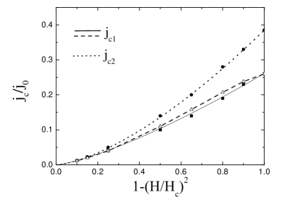
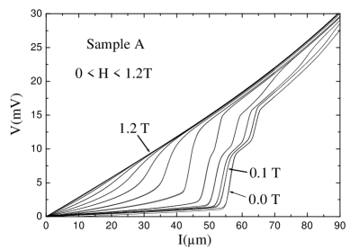
Finally, we present our results on the influence of an applied magnetic field on the I-V characteristics. We limit ourselves to data for sample A in the current driven regime (see Fig. 15). These results already support our theoretical predictions of Section IIb. It is evident that the lower critical current density decreases with increasing applied magnetic field. From some range of H-values only one jump in the voltage exists. We explain it by an increase of at relatively large magnetic fields and hence there is a lack in space for the coexistence of two phase slip centers in the nanowire. At high magnetic fields the order parameter is strongly suppressed by H and the effect of quantum phase-slip fluctuations becomes more pronounced. This is the reason for a smoothing of the I-V characteristics at high magnetic fields.
IV Discussion
In conventional superconductor near Tc the N-S boundary conditions (in the sense mentioned in Sec. IIa) are valid Hsiang . For the bridge boundary conditions are more applicable due to Andreev reflections at the border between the normal metal and the superconductor Andreev ; Hsiang . At intermediate temperatures we expect a mixture of the N-S and bridge boundary conditions. It means that part of the voltage will drop at the boundaries and part in the sample. The situation in our experiment is even more complicated because in our two-point measurements there is also a voltage drop at the contacts. Probably, this will not allow us to observe the oscillations of the current in the voltage driven regime. Another reason is that our samples are very long compared to (even for our 22 sample ) and consequently the amplitude of the oscillations is very small. But nevertheless our calculations in both limiting cases of bridge and N-S boundary conditions predicts an S-shape of the I-V characteristic.
We found that the type of boundary conditions are not so important for the process of nucleation of phase slip centers if the length of the sample is much larger than . However, the difference in the process of the conversion of superconducting electrons to normal ones and vice versa at the N-S boundary at various temperatures plays a crucial role for the creation of phase slip centers in shorter nanowires. It turned out that for similar parameters (nanowire’s length, coherence length, superconducting gap, ) phase slip centers appear in the superconducting wire at smaller currents for the case of the bridge geometry boundary conditions.
All our theoretical results are strictly speaking only valid near , which is the temperature region where Eqs. (1,2) are quantitatively correct. Nevertheless, experimental results supports our prediction on the competition of two relaxation times in the creation of a phase slip center even far from . Indeed, an applied parallel magnetic field decreases the lower critical current (compare Fig. 15 and Fig. 4). Jumps in the voltage turned out to be almost an independent function of the disorder (of the resistance of the sample) as it follows from theory. Unfortunately, it is rather difficult to check the dependence of on the length of the nanowire using our technique because every preparation of a new sample leads to a different level of disorder and hence different values for and .
Therefore, we expect only quantitative differences in the dependence of , , as compared with our theoretical results. Some qualitative differences (see Ref. Baratoff ) in the dynamic of the order parameter at the phase slip center or the creation of charge imbalance waves Kadin2 cannot affect the main properties of our theoretical results because it does not influence the existence of the two different critical currents: and . It may lead to quantitative differences in the dependence of and on the microscopic parameters of the superconductor.
Finally, we would like to discuss other mechanisms which, for our geometry, may lead to an S-behavior of the I-V in the V=const regime. The first is heating Volkov . In order to explain the double S-structure for our samples A, B by this mechanism we have to assume that heat dissipation and heat evacuation have a very complicated and non trivial dependence on temperature. We do not know any mechanisms which can lead to such adependence in our case. Besides we did not any observe hysteresis in the current driven regime which is an inevitable property of that mechanism if the I-V characteristic would have a S-shape in the voltage driven regime. For these reasons we believe that heating is not responsible for the observed behavior.
Secondly, if the nanowire contains a normal region the I-V characteristic will exhibit an S-behavior due to multiple Andreev reflection in the SNS structure Nicolsky . We do not have any indication for this process from our R(T) and R(H) measurements which shows that our samples are quite homogeneous. Furthermore the structure would occur at voltages much smaller than . In our case the S-behavior is seen for - see Fig. 13 (for Pb, ). Andreev reflection on the N-S boundaries may give rise to a zigzag shape of the I-V in the V-const regime Sols but this effect is negligible for our samples with .
Acknowledgements.
This work was supported by IUAP(P5/1/1), GOA (University of Antwerp), ESF on ”Vortex matter”, the Flemish Science Foundation (FWO-Vl) and the ”Communauté Française de Belgique” through the program ”Actions de Recherches Concertées”. D.V. is supported by DWTC to promote S T collaboration between Central and Eastern Europe. We thank the POLY lab. at UCL for the polymer membranes. S. Michotte is a Research Fellow of the FNRS.References
- (1) M. Thinkham, Introduction to superconductivity, (McGraw-Hill, NY, 1996), Chpt. 11.
- (2) V. V. Schmidt, The Physics of Superconductors, (Springer-Verlag, Berlin, 1997), Chpt. 7.
- (3) J. S. Langer and V. Ambegaokar, Phys. Rev. 164, 498 (1967).
- (4) B.I. Ivlev and N.B. Kopnin, Adv. Phys. 33, 80 (1984).
- (5) R. Tidecks, Current-induced nonequilibrium phenomena in quasi-one-dimensional superconductors, (Springer, Berlin, 1990).
- (6) J.D. Meyer and G.V. Minnigerode, Phys. Lett. 38A, 529 (1972).
- (7) J. D. Meyer, Appl. Phys. 2, 303 (1973).
- (8) W. J. Skocpol, M. R. Beasley, and M. Tinkham, J. Low Temp. Phys. 16, 145 (1974).
- (9) G.J. Dolan and L.D. Jackel, Phys. Rev. Lett. 39, 1628 (1977).
- (10) D. Y. Vodolazov and F. M. Peeters, Phys. Rev. B 66, 054537 (2002).
- (11) B. A. Malomed and A. Weber, Phys. Rev. B 44, 875 (1991).
- (12) D.Y. Vodolazov, F.M. Peeters, L. Piraux, S.Mátéfi-Tempfli, and S. Michotte, (cond-mat/0304193) Phys. Rev. Lett. (2003).
- (13) L. Kramer and R.J. Watts-Tobin, Phys. Rev. Lett. 40, 1041 (1978).
- (14) L. Kramer and A. Baratoff, Phys. Rev. Lett. 38, 518 (1977).
- (15) R. J. Watts-Tobin, Y. Krähenbühl, and L. Kramer, J. Low Temp. Phys. 42, 459 (1981).
- (16) A.M. Kadin, W.J. Skocpol, and M. Tinkham, J. Low Temp. Phys. 33, 33 (1978).
- (17) T.Y. Hsiang and J. Clarke, Phys. Rev. B 21, 945 (1980).
- (18) A. Schmid and G. Schön, J. Low Temp. Phys. 20, 207 (1975).
- (19) For our parameters so that in order to prevent the appearance of several phase slip centers simultaneously when we put a small defect (of first type with - see discussion in the text on the effect of defects on the phase slip process) in the center of the sample in order to provide the existence of only one PSC in the wire.
- (20) L. Kramer and R. Rangel, J. Low Temp. Phys. 57, 391 (1984).
- (21) V. L. Ginzburg, Zh. Eksp. i Teor. Fiz. 34, 113 (1958) [Soviet Phys. - JETP 7, 78 (1958)].
- (22) D. H. Douglass, Jr., Phys. Rev. 124, 735 (1961).
- (23) D. Y. Vodolazov, F. M. Peeters, S. V. Dubonos, and A. K. Geim, Phys. Rev. B 67, 054506 (2003).
- (24) S. Michotte, S.Mátéfi-Tempfli, and L. Piraux, Appl. Phys. Lett. 82, 014324 (2003).
- (25) N. Giordano, Phys. Rev. B 41, 6350 (1990); ibid. 43, 160 (1991).
- (26) C.N. Lau, N. Markovic, M. Bockrath, A. Bezryadin, and M. Tinkham, Phys. Rev. Lett. 87, 217003 (2001).
- (27) S. Dubois, A. Michel, J.P. Eymery, J.L. Duvail and L. Piraux, Jour. Mater. Res. 14, 665 (1999).
- (28) It is interesting to note that if in a short sample two PS centers may appear and the differential resistance will practically not change after every voltage jump and should be approximately equal to the normal one if . The change in the voltage will probably only be connected in this case with a change in the coefficient , because in short nanowires the PSC should strongly interact with each other. If the coefficient does not change it would be quite difficult to notice the appearance of the second phase slip center.
- (29) A.F. Andreev, Zh. Eksp. Teor. Fiz. 46, 1823 (1964) [Sov. Phys. JETP 19, 1228 (1964)].
- (30) A. Baratoff, Phys. Rev. Lett. 48, 434 (1982).
- (31) A.M. Kadin, L.N. Smith, and W.J. Skocpol, J. Low Temp. Phys. 38, 497 (1980).
- (32) A.F. Volkov and Sh.M. Kogan, JETP Lett. 19, 4 (1974).
- (33) R. Kümmel, U. Gunsenheimer, and R. Nicolsky, Phys. Rev. B 42, 3992 (1990).
- (34) J. Sánchez-Canizares and F. Sols, J. Low Temp. Phys. 122, 11 (2001).