First-principles calculations of strontium on Si(001)
Abstract
This paper reports state-of-the-art electronic structure calculations on the deposition of strontium on the technologically relevant, (001) orientated silicon surface. We identified the surface reconstructions from zero to four thirds monolayers and relate them to experimentally reported data. A phase diagram is proposed. We predict phases at 1/6, 1/4, 1/2, 2/3 and 1 monolayers. Our results are expected to provide valuable information in order to understand heteroepitaxial growth of a prominent class of high-K oxides around SrTiO3. The insight obtained for strontium is expected to be transferable to other alkaline earth metals.
pacs:
68.43.Fg, 68.47.Fg, 71.15.Mb, 73.20.-rI Introduction
Device scaling has been the engine driving the microelectronics revolution as predicted by Moore’s law.2 By reducing the size of transistors, processors become faster and more power efficient at an exponential rate. Currently the main challenge in device scaling is the integration of high-K oxides as gate oxides into silicon technology.
The gate oxide is the dielectric of a capacitor, which is used to attract charge carriers into the channel region. Thus a current can flow from source to drain, provided a voltage is applied to the gate electrode. With a thickness of only 1-2 nm3 the gate dielectric is the smallest structure of a transistor. As the thickness of the gate oxide is further reduced, its insulating property is lost due to direct tunneling through the ultrathin oxide. The results are intolerable leakage currents and a large power consumption.
A remedy to this problem is the replacement of the current SiO2 based gate oxides with an insulator having a larger dielectric constant, a so-called high-K oxide. A high-K oxide gate with the same capacity as an ultrathin SiO2 based one will be thicker and should therefore exhibit smaller leakage currents due to direct tunneling. The integration of new oxides into the semiconductor technology has, however, proven to be a major problem. Hence an enormous research effort is underway to understand growth of high-K oxides onto silicon.
Currently, HfO2 and ZrO2 are the main contenders for the first generation of high-K oxides to be introduced in fabrication. These oxides still exhibit an interfacial SiO2 layer and therefore do not form a direct interface with silicon. As scaling proceeds, an interfacial SiO2 layer cannot be tolerated anymore. The existence of an atomically abrupt interface between silicon and a high-K oxide has been demonstrated by McKee et al.4, 5 for BaxSr1-xTiO3 on Si(001), after an epitaxial relationship has been reported in the late 80’s.6, 7
A detailed understanding of metal adsorption is crucial to control oxide growth on Si. The growth process is guided by the sequence of structures that develop as the metal is deposited on the silicon surface.4 The nature of these structures as well as the interface between Si and a high-K oxide is, however, still under debate.
The adsorption of the alkaline earth metals Sr and Ba on Si(001) has been extensively studied. Most of the studies of Sr on Si(001) are diffraction studies such as low-energy electron diffraction (LEED) 8, 9, 10, 11, 12, 13 and reflection high-energy electron diffraction (RHEED) 14, 15, 16, 17 or scanning tunneling microscopy (STM) 9, 10, 13 experiments. The STM studies have been most valuable because they contribute detailed real-space information on the atomic scale. Similar LEED,18, 19, 20 RHEED 21 and STM 22, 23, 24, 25, 26 as well as x-ray photoemission studies 27, 20 have been performed for Ba. X-ray standing wave experiments provide valuable restrictions on the structures with coverages of 1/2 and 1/3 monolayer (ML).28 The photoemmision (XPS) 29, 12 studies provide insight into the ionization state of Sr, and show a qualitative change of the Fermi-level pinning as a function of coverage.12
Diffraction studies suffer from the fact that they average over several structures and terraces. Here STM experiments provide valuable clues. One of the major experimental difficulties is the determination of the coverage at which the data are collected.12
Theoretical investigations of isolated Ba atoms adsorbed on Si(001) have been performed by Wang et al.30
In this work we address the deposition of Sr on Si(001) using state-of-the-art electronic structure calculations. We attempt to provide a complete set of adsorption structures, their energetics, chemical binding and electronic structure. We will categorize the reconstructions by pointing out the driving forces that lead to the various ordered structures. This provides a unified picture of Sr adsorption from low coverage up to 4/3 monolayers.
II Computational details
The calculations are based on density functional theory31, 32 using a gradient corrected functional.33 The electronic structure problem was solved with the projector augmented wave (PAW) method,34 an all-electron electronic structure method using a basis set of plane waves augmented with partial waves that incorporate the correct nodal structure. The frozen core states were imported from the isolated atom. For the silicon atoms we used a set with two projector functions per angular momentum for and -character and one projector per angular momentum with -character. The hydrogen atoms of the back surface had only one -type projector function. For strontium we treated the 4 and 4 core shells as valence electrons. Per angular momentum we used three -type and two - and -type projector functions. The augmentation charge density has been expanded in spherical harmonics up to . The kinetic energy cutoff for the plane wave part of the wave functions was set to 30 Ry and that for the electron density to 60 Ry.
A slab of five silicon layers was used as silicon substrate. Wang et al.30 report that the adsorption energy of a Sr atom on the surface changes by 0.05 eV when between a 4-layer slab and a 6-layer slab of silicon. In our calculations the energy per additional silicon atom agrees to within 0.06 eV with that of bulk silicon between a 4-layer and a 5-layer slab. The dangling bonds of the unreconstructed back surface of the slab have been saturated by hydrogen atoms. The lateral lattice constant was chosen as the experimental lattice constant Å of silicon.35 The slabs repeat every 16 Å perpendicular to the surface, which results in a vacuum region of 9.5 Å for the clean silicon surface.
The Car-Parrinello ab-initio molecular dynamics36 scheme with damped motion was used to optimize the electronic and atomic structures. All structures were fully relaxed without symmetry constraints. The atomic positions of the backplane of the slab and the terminating hydrogen atoms were frozen.
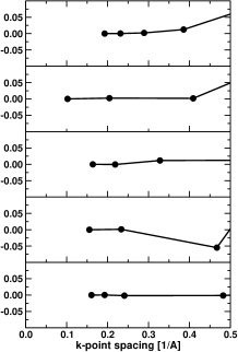
Many of the Sr adsorption structures are metallic which requires a sufficiently fine grid in k-space. We used an equivalent to eight by eight points per surface unit cell. This value has been chosen after careful convergence tests for surface structures, bulk silicon and bulk Sr silicides (Fig. 1). In cases where this k-mesh is incommensurate with the size of the unit cell we selected the closest, finer commensurate k-mesh.
For metallic systems, the orbital occupations were determined using the Mermin functional38 which produces a Fermi-distribution for the electrons in its ground state. The electron temperature was set to 1000 K. In our case this temperature should not be considered as a physical temperature but rather as a broadening scheme for the states obtained with a discrete set of k-points. The Mermin functional adds an entropic term to the total energy, which is approximately canceled by taking the mean of the total energy and the Mermin-free energy as proposed by Gillan:39
| (1) |
In order to express our energies in a comprehensible manner, we report all energies relative to a set of reference energies. This set is defined by bulk silicon and the lowest energy polymorph of SrSi2 . The reference energies are listed in Tab. 1. The reference energy Sr for a Sr atom, corresponding to the coexistance of bulk silicon and bulk SrSi2, is extracted from the energy E[SrSi2] of the disilicide calculated with a k-mesh and the reference energy of bulk silicon as
| (2) |
The bulk calculation for silicon was performed in the two atom unit cell with a () k-mesh and at the experimental lattice constant of 5.4307 Å.35
| Energy [H] | |
|---|---|
| [Si] | -4.0036 |
| [Sr] | -31.1441 |
| [5 layer-Si-slab] | -21.1140 |
| [4 layer-Si slab] | -17.1083 |
For the surface calculation, we always subtracted the energy of a clean () silicon surface of the same slab thickness, to account for slab including hydrogen termination. For the surfaces with half a monolayer coverage of silicon we assumed that the corresponding reservoir for the silicon atoms is a silicon terrace. Hence, the reference energy for the 4.5 layer silicon slab is the average energy of a 4-layer slab and a 5-layer slab. The terrace energy itself does not enter the limit of an infinitely dilute step density.
In some of our structures the choice of unit cell has an impact on the dimer buckling. We estimated the energy of a buckling reversal from the energy difference of a and a supercell. The cell with an odd number of dimers contains one buckling reversal. The calculated energy for such a buckling reversal is 0.06 eV.
III Bulk Silicides
Before studying the adsorption of Sr on silicon we investigated the bulk silicides of Sr. The energetics of bulk silicides provide us with the driving force to go from ordered surfaces structures to silicide grains on the surface. Our calculations on early transition metals on silicon indicate that silicide formation is a major problem for layer-by-layer growth of an oxide.40
The binding characteristics of the bulk silicides provide us with insight into the favored structural templates which might be anticipated for the Sr-covered silicon surface.
Sr-silicides are typical Zintl compounds. According to the Zintl-Klemm concept,41 atoms with an increased number of electrons form similar structures as atoms with the correspondingly increased atomic number. Consequently, a charge transfer of one electron to silicon will result in a preferred bonding environment similar to phosphorous with three or five covalent bonds. Addition of two electrons will result in chain-like structures like sulfur. After addition of three electrons one anticipates formation of dimers and once four electrons are transfered, isolated ions are expected. In other words: for every added electron one covalent bond will be missing.
Due to the large difference in electronegativity, Sr formally donates its two valence electrons to the silicon substrate.
-
•
In SrSi2 one electron is transfered per silicon atom. Hence three-fold coordinated silicon networks are formed as shown in the top two structures of Fig. 2.
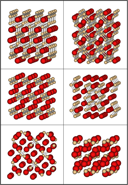
Figure 2: Bulk silicide structures. Top left: SrSi2 42; Top right: SrSi2 43; Middle left: SrSi 44; Middle right: SrSi 45; Bottom left: Sr5Si3 46; Bottom right: Sr2Si ()47. The large, dark spheres represent Sr atoms, the smaller, light spheres Si atoms. Energies are listed in Tab. 2. -
•
Two electrons are transfered in SrSi so that the silicon network is similar to that of elemental sulfur with two-coordinated silicon atoms forming Si chains as seen in the middle left panel of Fig. 2. The middle right panel shows another modification of SrSi. The average number of covalent bonds per silicon atom is, however, still two.
-
•
In Sr5Si3 there is a charge transfer of 10 electrons to three silicon atoms, which can be used to form two Si3- ions and one Si4- ion. The two Si3- combine to form dimers and the Si4- is no more able to form covalent bonds. Hence we observe an equal number of Si dimers and single Si ions in the structure of Sr5Si3 as shown in the lower right panel of Fig. 2.
-
•
In Sr2Si four electrons are transfered to each silicon atom. As a consequence, the Si atoms in the stucture on the bottom right of Fig. 2 do not form covalent bonds.
We find SrSi2 to be the most stable phase of silicides per Sr atom (Tab. 2). Therefore we have chosen this material to define, together with bulk Si, the reference energy for Sr.
| E[Sr] [eV] | |
|---|---|
| SrSi2 | 0.00 |
| SrSi2 | 0.01 |
| SrSi | 0.09 |
| SrSi | 0.20 |
| Sr5Si3 | 0.39 |
| Sr2Si () | 0.45 |
As a side remark, we note that a lower energy of a Sr atom in a bulk silicide compared to the adsorbed Sr on the surface does not automatically indicate the formation of silicide grains during growth: The silicide formation may be suppressed by the strain due to an epitaxial constraint by the silicon lattice constant. Thus the formation of silicides is expected to be delayed for thin films, because the bulk silicides have a large mismatch with the silicon substrate. This argument does not refer to the thermodynamic equilibrium of large samples, but it indicates that nucleation of silicide grains will have to overcome a large barrier.
IV The clean silicon surface
The clean (001) silicon surface has a dimer-row reconstruction. We briefly summarize the driving forces towards this reconstruction in order to understand the adsorption structures of Sr on silicon.
An unreconstructed surface of silicon (001) is terminated by a square, () array of atoms. Each silicon atom on the surface is connected by two bonds to the subsurface. Consequently, there are two half-occupied dangling bonds on each silicon sticking out of the surface.
Each pair of surface silicon atoms forms a dimer bond which saturates one of the two dangling bonds on each atom. The dimers arrange in rows. This is the so-called dimer row reconstruction which results in an energy gain of 0.65 eV per unit cell according to our calculations.
In a second reconstruction, both electrons in the dangling bonds localize on one atom of each dimer, resulting in a dimer buckling. The buckling is driven by the fact that a sp3 hybridization is favored for a five-electron species such as the negative Si atom, while a sp2 hybridization is favored for a 3-electron species such as the positive silicon atom. The sp2 hybridization in turn favors a planar bonding environment, whereas three-coordinated sp3 bonded atoms form an umbrella like environment. In the buckled-dimer row reconstruction, the electrons are localized on the atoms sticking out farthest from the surface. The dimer buckling can be considered as a Peierl’s distortion which splits the half-filled energy bands resulting from the dimer bonds into a filled and an empty band, with a band gap in between. The energy gain due to this distortion is 0.12 eV per cell.
The energies quoted here are in reasonable agreement with previously published LDA pseudo-potential calculations.48 The dimer reconstruction can be considered to be fairly stable. Even at 1500 K only 3% of the dimer bonds are broken as estimated from the Boltzmann factor with eV.
Two neighboring buckled dimer rows interact only weakly. We obtain an energy difference of 1.2 meV per dimer between the reconstruction with anti-parallel buckling and the reconstruction with parallel buckling on neighboring dimer rows. This indicates that the buckling patterns of different rows are fairly independent of each other.
Within a row, however, the buckling of the dimers is coupled in an anti-correlated manner. This can, at least partly, be explained by the fact that the lower silicon atom of a dimer pushes the two adjacent subsurface silicon atoms apart. For the equivalent silicon atom of the next dimer, it is therefore favorable to be in the higher, sp3-like configuration.49
There has been an intense debate as to whether there is dimer buckling or not. STM images reveal a structure. They exhibit the buckling only at rather low temperatures and near defects. The theoretical predictions depend strongly on the approach chosen (cluster calculations with configuration interaction or density functional calculations with periodic boundary conditions). The most conclusive results have been produced by Quantum Monte Carlo (QMC) simulations50 indicating that the buckling is present and density functional calculations just overestimate the energy difference.
The fact that STM experiments cannot resolve the dimer buckling may be due to thermal averaging of the two buckled configurations. We believe that the mechanism is due to the migration of a soliton-like defect in the anti-correlated buckling pattern of a dimer row. The calculated energy for this defect is 0.06 eV (see section II). Thus we predict a concentration of one such defect per 11 dimers at room temperature. Typical tunnel currents in STM experiments are around 1 nA, which corresponds to six electrons per nanosecond.
Thus even a soliton migration barrier as large as 0.05 eV would imply that the buckling changes once during the transfer of a single electron. These estimates should be taken with caution, since the small energy difference of 0.06 eV carries a large relative error bar.
From the comparison between DFT and Quantum Monte Carlo calculations one can deduce an error bar of 0.05 eV per () unit cell due to electron correlations.50 We verified that this correction does not qualitatively affect the findings reported in this paper.
V Isolated Sr on silicon
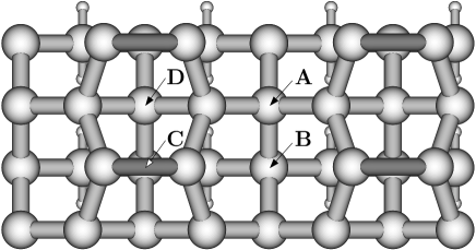
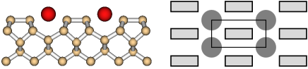
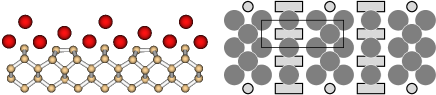
In order to determine the low-coverage limit of Sr-adsorption we investigated the energy as a function of the lateral position of a Sr ad-atom on the surface. The total energy as a function of the lateral position of Sr is obtained by constraining the lateral movement of the Sr-atom relative to the rigid back plane of the slab. The calculations were performed in a surface super cell. We considered the high symmetry points of the (2) surface shown in Fig. 3 and the mid-point between the local minima. The energies of the high symmetry positions are given in Table 3.
| Position | [eV] |
|---|---|
| A | 0.00 |
| B | 0.55 |
| C | 0.75 |
| D | 0.29 |
| A–D midpoint | 0.61 |
Sr has the global minimum at position A as defined in Fig. 3. Sr is located in the trench between the dimer rows and in the center of 4 surrounding dimers. The Sr atoms are slightly elevated above the plane of the surface dimers.
A metastable position, D of Fig. 3, is located in between two dimers on top of a dimer row. It is 0.29 eV higher in energy than the global minimum. We will see that the structures A and D are repeating motifs in a range of different adsorption structures.
The diffusion of Sr on the silicon surface proceeds about equally fast parallel and perpendicular to the dimer rows, with a slight preference for the parallel direction. The diffusion barrier along the valley is equal to the energy difference between sites A and B, namely 0.55 eV, the one across the row is 0.61 eV and is estimated by the midpoint between the sites A and D
It should be noted that in our analysis we ignored the reduced symmetry due to dimer buckling. As a result, different versions of the high symmetry points quoted here exist with slightly different energies. For the structure A we found two versions which differ in energy by 0.15 eV. In these cases the lowest energy structure has been chosen.
In contrast to Sr, there has been a lot of work related to isolated Ba atoms adsorbed on Si(001).30, 22 Our results are in line with previous calculations for isolated Ba on Si(001).30 We believe that both atoms behave in a similar fashion. Ba has been found mostly on sites A in the trenches, but also on sites D on top of the dimer rows. The main difference between Ba and Sr lies in the energy difference between the two metastable sites A and D. For Ba the difference is 0.88 eV 30 which is substantially larger than the 0.29 eV for Sr.
The chemical binding can be well understood in an ionic picture as suggested by the chemical binding of the silicides. The two electrons of the Sr atom are donated into an unoccupied dangling bond of a Si dimer. Interestingly we find this electron pair to be localized at a single dimer. This is evident from the dimer buckling, which vanishes when both dangling bonds are occupied.
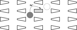
The Sr atom experiences an additional electrostatic stabilization from the remaining three buckled dimers next to it. They are buckled such that the negative, and therefore raised, silicon atoms are located next to the Sr atom. The local configuration is shown in Fig. 4. This arrangement significantly affects the buckling of the two dimer rows adjacent to the Sr atom: (1) the buckling gets pinned and is therefore observed in STM images in the vicinity of a Sr atom whereas it is thermally averaged out on the bare surface; (2) the dimer buckling within one row is reversed as already pointed out by Wang et al.30 This becomes apparent by looking at the row left of the Sr atom in Fig. 4.
From the static structure shown in Fig. 4 it is not evident why both dimer rows contain a buckling reversal as observed in Fig. 1 b) of Yao et al.22 We attribute the experimental observation to a dynamical effect: One electron pair can rapidly migrate from the filled dimer to one of the three buckled dimers next to the Sr ad-atom. If this fluxional motion occurs on a time scale faster than the time scale for a buckling reversal of the entire chain, the buckling will appear pinned in both dimer rows.
In our super cell with an even number of dimers in a row, every reversal of the buckling must be compensated by a second one, thus artificially destabilizing the site A. This adds an uncertainty of up to 0.12 eV to all energies for the isolated Sr. Even taking this uncertainty into account, isolated Sr ad-atoms do not form a thermodynamically stable phase at any coverage as will be demonstrated in the next section.
VI Chain structures at dilute coverages
The Sr-atoms on the surface tend to arrange in chains, as seen in the STM experiments.9, 10 Similar results have been obtained for Ba on Si(001).23
Our calculations predict random, single chain structures up to a coverage of 1/6 ML. Between 1/6 ML and 1/4 ML we find condensed, single and double chain structures. Above 1/4 ML the multiple chain structures convert into disordered arrays of double vacancies as will be discussed below. We investigated chain structures with coverages of 1/16, 1/10, 1/8, 1/6, 1/4, 3/10, 1/3, 5/14 and 6/16 ML. We find an energy gain of 0.3 to 0.4 eV per Sr atom when single chains are formed from isolated Sr ad-atoms on A-sites.
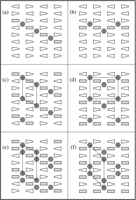
| Sr coverage | Figure number | Energy/Sr [eV] |
| 1/ | 5(a) | just schematic |
| 1/ | 5(b) | just schematic |
| 1/6 | 5(c) | -1.15 |
| 1/6 | 5(d) | -1.15 |
| 1/4 | 5(e) | -1.10 |
| 1/4 | 5(f) | -1.06 |
| 1/4 | 14 bottom | -0.30 |
| 1/4 | 14 top | 0.44 |
| 1/2 | 9 | -0.92 |
| 2/3 | 11 left | -0.74 |
| 1 | 10 left | 0.04 |
| 1 | 10 right | 0.08 |
| 1 | 11 right | -0.12 |
| 4/3 | 13 | 0.28 |
The chain formation is driven by the electrostatic attraction between the positively charged Sr-ions, located at A-sites, and the negatively charged dimers: An isolated Sr ion located at an A-site, with the lone pairs of the four neighboring dimers pointing towards it, donates its two valence electrons into a silicon dangling bond adjacent to a neighboring valley. Thus it offers a preferred binding site for a Sr atom in that valley, namely next to this filled dangling bond as seen in Fig. 4. This second atom in turn donates its electron pair to the dimer row which does not already contain a negatively charged dimer and all four surrounding dimers will rearrange to point their lone pairs towards the new ad-atom. This process continues to form chains of Sr atoms. The filled dimers are clearly identified by the absence of any buckling.
Two nearest Sr ions of one chain are displaced parallel to the dimer row by one lattice constant in order to position the filled dimer inbetween. Since the favorable Sr positions are staggered with respect to the dimers, the chains run at an angle of 30 degree relative to the direction of a dimer or 60 degree with respect to the dimer rows. The small energy difference of 0.02 eV per Sr ion between diagonal and zig-zag chains at e.g. 1/8th ML cannot be considered as a hard number due to the systematic errors of DFT calculations. It does, however, indicate that the energy cost for changing the direction of such a chain is negligible so that these chains may meander on the surface.
As for the isolated Sr ad-atom, an additional stabilization occurs due to the dimer buckling of the surrounding silicon dimers. The negatively charged, raised part of an adjacent dimer is located next to the Sr-ion, stabilized by electrostatic and covalent interactions. Reversing the buckling of one of the dimers next to a Sr ion raises the energy by 0.38 eV.51 This ordering induces a freezing of the dimer buckling, which reaches far out into the clean silicon surface, as can be clearly seen in the STM images by Hu et al.23
At first sight one might think that there is a second preferred binding site in Fig. 4, right next to the initial ad-atom on the A site below the open circle. This configuration is, however, only possible for a pair of Sr atoms. A further continuation of such a chain perpendicular to the dimer row will make it impossible to rearrange dimers in a way that only filled dangling bonds are oriented towards the ad-atoms. Such chains are therefore destabilized with respect to diagonal or zig-zag ones.
A favorable registry between two Sr-chains is obtained if the Sr atoms are either in contact or separated by an even number of vacant A sites along each valley of the Si-surface. This follows from a simple building principle which is an extension of what is already known from isolated chains:
-
•
Each Sr atom is electrostatically stabilized by four negatively charged silicon atoms located next to it. Negative silicon atoms have two electrons in their dangling bond and are in a raised, -like bonding configuration.
Violation of this rule raises the energy by 0.38 eV per empty dangling bond next to the Sr atom. At this level of abstraction we do not distinguish between a negatively charged Si atom of a buckled and an unbuckled dimer.
-
•
There are no reversals of the dimer buckling in the Sr-free regions on the surface. A buckling reversal increases the energy by 0.06 eV. This is a consequence of the anti-correlated coupling of the dimer buckling within one row (see section IV).
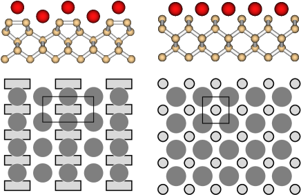
When the chains approach the shortest possible distance before they collapse into double chains, we obtain a partially ordered structure at 1/6 ML as shown in Fig. 5 (c) and (d). It should be noted that our calculations indicate that also the condensed chains at 1/6 ML change their directions frequently, even though synchronized with the neighboring chains running in parallel.
As the coverage increases, Sr atoms arrange themselves into double chains as shown in Fig. 5(e), resulting in a partially ordered surface structure at 1/4 ML. The ”12” areas in Fig. 4 of Ojima et al.25 can be explained by double chains at a 1/4 ML. Their interpretation that buckled Ba dimers at 1/2 ML coverage are responsible for this ”wavy structure” cannot be supported by our calculations.
If we continue this building principle beyond 1/4 ML we will obtain sequences of triple, quadruple, etc., chains of Sr atoms separated by double vacancies. However, the positions of the double vacancies of different valleys are then only weakly correlated. Double vacancies of neighboring valleys can arrange themselves almost arbitrarily except that they do not line up perpendicular to the dimer rows. This implies a new building principle of double vacancies that do not necessarily arrange in chains. Note that a multiple chain structure of Sr atoms can also be interpreted as a chain structure of double Sr vacancies. This building principle can already be observed in Fig. 5(e) and (f) for 1/4 ML, which show that double vacancies in neighboring valleys can assume three out of four relative positions. While the energy difference between the structures in Fig. 5(e) and (f) is as small as 0.04 eV per Sr atom, it decreases further for the analogous structural patterns for wider Sr-chains. For coverages close to one-half ML, when the concentration of double vacancies is dilute, we therefore expect a nearly random arrangement of double vacancies instead of multiple chains.
The reciprocal lattice vectors for the diagonal chain structures are and , where is the periodicity of the the real space unit cell (compare Figs. 5(c) and (e)) along the dimer row direction. It should be noted that there is some structural disorder due to frequent changes in the chain direction. For zig-zag chains the corresponding reciprocal lattice is spanned by the vectors and . The actual diffraction pattern observed in experiment will contain a mixture of both reciprocal lattices.
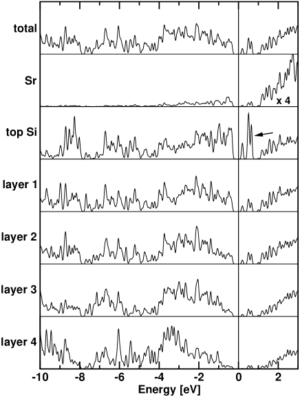
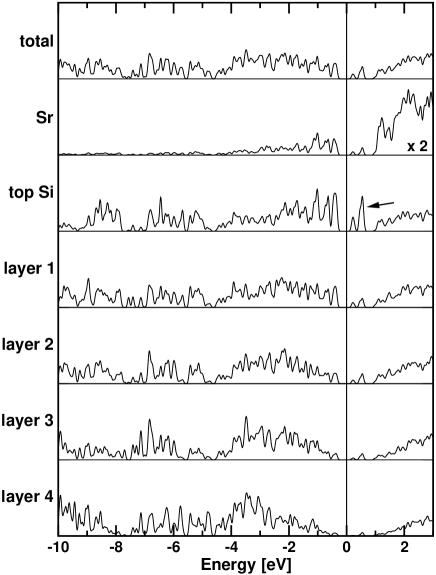
The density of states of the single chain structure at 1/6 ML is shown in Fig. 6. The states on the Sr atom, which appear in the valence band, can be attributed to the tails of the Si dangling bonds, which hybridize with the Sr- orbital. We observe states in the Si band gap, which are assigned to the empty dangling bonds on the buckled dimers. These states actually form a single band that is separated from the valence and conduction bands. The fact that they appear as individual states is an artifact of our discrete sampling of the Brillouin zone. This band pins the Fermi level in the lower part of the band gap. This feature remains nearly unchanged in the density of states of the double chain structure at 1/4 ML (Fig. 7). It disappears, however, with the absence of the half-occupied dimers at 1/2 ML as seen in Fig. 8. Thus the gap states remain approximately in their position as the coverage increases, but the density of states is reduced. Hence the Fermi-level will remain pinned in the lower part of the silicon band gap up to a coverage of 1/2 ML. At this point the Fermi-level becomes unpinned. In the following we will see that for coverages above 1/2 ML states from the conduction band are pulled into the band gap of silicon, and pin the Fermi level in the upper part of the band gap.
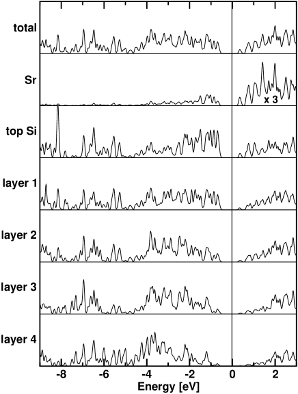
This finding explains the discontinuity of the band-bending as observed by Herrera-Gomez et al.12 Their XPS studies show that the Fermi level shifts up by almost 0.5 eV when the coverage is increased from below 1/2 ML to above. However, it should be noted that such a discontinuity in Fermi-level pinning is not specific to detailed structures: also higher energy structures exhibit a similar behavior.
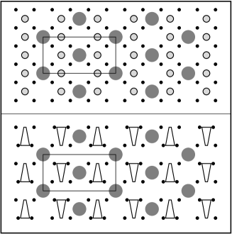
VII The reconstruction at 1/2 ML
At a coverage of 1/2 ML all dangling bonds of the surface dimers are fully occupied (Fig. 9). It can be considered as the canonical Sr-covered Si surface. It is the only Sr-covered surface structure without states in the band gap of silicon. This structure is ”isoelectronic” to an hydrogen terminated silicon surface and is therefore expected to be comparably inert. The increased resistance to oxidation has already been observed experimentally.13 A reconstruction at 1/2 ML has already been reported by several authors.8, 52, 18, 12, 15
This structural template has been proposed to be the basic building block of the interface between silicon and SrTiO3.53
VIII From 1/2 ML to 1 ML
For coverages between 1/2 ML and 1 ML, we find structures built up from three structural templates:
When we increase the coverage above 1/2 ML, the additional atoms occupy the D-sites, since all A-sites are already occupied. When all A-sites and all D-sites are occupied, as shown in the left panel of Fig 10, the coverage is that of 1 ML. At this coverage, two electrons are transferred to each silicon atom instead of only one as in case of the 1/2 ML. These electrons can fill the dimer antibonding states and thus break up the dimer bond. When all dimer bonds are broken at 1 ML we obtain a reconstructed silicon surface with a Sr-ion above the center of each square of silicon atoms (Fig. 10 right). This structure is, however, never realized in its pure form due to the large strain in the top layer. An indication for the strain is the difference between the spacing of Sr atoms in bulk SrSi (Fig. 2) and that of this hypothetical surface structure. The former is larger by 25 %. Nevertheless, this pattern is found as a building block in a number of low-energy structures between coverages of 0.5 ML and 1 ML. The reconstruction at 1 ML is unfavorable by 0.04 eV per Sr atom compared to the corresponding structure.
By combining the structure at 1/2 ML (Fig. 9) and the structure at 1 ML (right panel of Fig. 10), a series of structures with increasing coverage and periodicity can be formed: dimer rows are separated by stripes of the ()/1 ML structure with increasing width. This leads to a series of structures at a coverage of ML. We have investigated these structures from to .
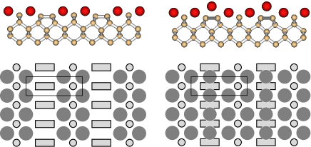
The first structure in the series is the reconstructed surface at a coverage of 2/3 ML shown in the left panel of Fig. 11. It consists of dimer rows separated by a stripe of two Sr atoms in the ()/1 ML configuration. According to our calculations this structure is present as a distinct phase between 0.5 ML and 1 ML.
In order to form this structure the dimer row pattern needs to reconstruct. This process is facilitated by the additional electrons in the conduction band which weaken the dimer bonds: beyond a coverage of 1/2 ML Sr is likely to act as a catalyzer for dimer bond rearrangement.
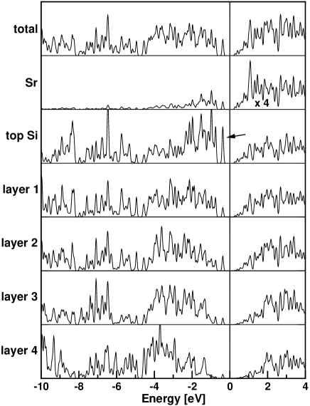
The density of states for this structure (Fig. 12) exhibits a surface band that ranges from the continuum of the valence band of bulk silicon into its bandgap. The surface band is localized on the dangling bonds of the silicon dimers and the undimerized silicon atoms. The Fermi level is pinned between this band and the conduction band of silicon (see also discussion in section VI).
For coverages greater than 2/3 ML, that is , the structures can be interpreted as stripes with coverage of 1 ML with a reconstruction separated by dimer rows without Sr, as discussed above. As the stripes with /1 ML increase in width, they build up strain, which can be released by forming dimer rows with Sr atoms on top (Fig. 10 left). This corresponds to a transition between both 1 ML structures shown in Fig 10. Since the energy difference between these structural variants is smaller than 0.04 eV per Sr atom, it is likely that they do not form distinct phases but transform into each other in a fluxional fashion.
At a coverage of 1 ML we find a series of structures built from the two structural templates in Fig. 10. In our calculations the (Fig. 11) and reconstructions are most stable and, within the theoretical error bar, degenerate. There is a slow increase in energy towards the and reconstructions which are less than 0.11 eV per Sr atom higher in energy.
IX Beyond 1 ML
Beyond 1 ML additional Sr atoms deposit on top of the silicon atoms in the stripes. The first commensurate structure is the structure at a coverage of ML shown in Fig. 13.
Fan et al. have observed a reconstruction at a coverage of 1.3 ML, Bakhtizin et al.9, 10 have published STM images with a periodicity for a coverage of 1.2 ML. There, alternating bright and dark stripes have been observed, which we attribute to the Sr atoms on top of the dimer rows (darker stripes) and those on top of the of the two-fold coordinated Si atoms (more prominent stripes).
X The structure at 1/3 ML
Diffraction and STM studies identify a reconstruction at 1/3 ML8, 52, 9, 10, 20, 23, 28, 13, 24, 25. The diffraction studies (LEED, RHEED) did not distinguish between the orientations parallel and perpendicular to the dimer rows as they average over multiple terraces. Most previous studies assumed that the direction of the surface unit cell is orientated parallel to the dimer rows.9, 10, 28, 54 However, the STM images of Hu et al.23 (Fig. 5) and Ojima et al.25 (Fig. 4) clearly show, that the axis is orthogonal to the dimer row direction. This is particularly evident from the images showing the phase boundaries between the reconstructed domains and chain structures. This observation implies that the dimer row pattern is disrupted.
Our lowest energy structures for this coverage are variants of the quadruple chain as described in section VI. We have been unable to determine a thermodynamically stable structure with a diffraction pattern at 1/3 ML.
Hu et al. 23 suggested two structures for 1/6 and 1/3 ML. We simulated both of them and found them energetically unfavorable compared to the corresponding chain structures by more than 0.61 eV per Sr atom. Despite various other attempts, we failed to arrive at a thermodynamically stable surface structure with this reconstruction.
This failure may be attributed to our inability to scan the entire phase space. However, one should also consider the possibility of co-adsorption of other elements such as hydrogen or oxygen, which may help to tie up the dangling bonds created by disrupting the dimer row pattern. These effects have not been considered in the present study.
For the sake of completeness we also studied the model for the 1/3 ML coverage with the direction parallel to the dimer row. It was lower in energy than the structures suggested by Hu et al. 23 Nevertheless it turned out 0.23 eV per Sr atom higher in energy than the quadruple chain structure.
XI SrSi2 surface layer
So far, we have discussed structures on a stoichiometric Si-surface. The atomic model for the interface between Si and SrTiO3 by McKee et al.,4 which can be seen in the top panel of Fig. 14, has inspired us to also investigate reconstructions with only 1/2 ML of silicon in the surface layer. Such a structure can in principle be formed by the migration of Si atoms or dimers from step edges onto the terraces. For a clean surface this process is clearly not energetically favorable. However, it cannot be excluded a priori that the presence of Sr stabilizes a surface with half a monolayer of silicon.
We started from the structure proposed by McKee et al.4 which consists of a quarter monolayer of Sr and half a monolayer of Si. In this structure the Sr atoms occupy every second A-site in the valleys, while the Si atoms deposit on top of the center of four subsurface Si atoms. We restricted our search to the periodicity reported by McKee et al.
We find a number of metastable structures, the most stable one (Fig. 14 bottom) differs substantially from the proposal by McKee et al. The half monolayer of silicon on the surface combines into dimers, a behavior already known from Si ad-atoms on Si(001).55 The Sr atoms occupy positions in the center of four such dimers.
The energy of this structure is, however, still higher by 0.80 eV per Sr ad-atom than our lowest energy structure at this coverage, namely double chains of Sr atoms. The energy was evaluated relative to the average of a 4-layer and a 5-layer slab, representing a terrace. This energy thus describes the process of adsorption of Sr and the decomposition of two terraces into a single terrace with an additional half-monolayer of silicon.
We consider the difference in formation energy of 0.80 eV per Sr atom, relative to our lowest energy structure at this coverage, as too large for this structure to be physically relevant.
XII Phase diagram
We now investigate which of the reported structures form at given experimental conditions. The thermodynamic stability is determined by the zero-Kelvin Gibbs free energy , where is the energy per Sr atom and is the number of Sr atoms. is the chemical potential of the Sr atom relative to our reference energy for Sr. The extrinsic quantities, such as energies and , as well as the atom numbers are measured per unit cell of the silicon surface. In Fig. 15 we show the adsorption energy per surface unit cell.
The thermodynamically stable phases are determined by connecting the points in Fig. 15 by line segments and forming the lower envelope. Each line segment corresponds to the coexistence of two phases, denoted by and , at the ends of the line segment with energies and and and Sr atoms per unit cell. For a coverage per unit cell between and , the energy is . The slope of the line segment, namely , is the chemical potential at which both phases and coexist. All structures not contributing to the lower envelope are not thermodynamically stable at low temperatures. At higher temperatures they may be stabilized due to entropic effects.
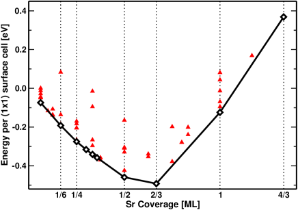

The one-dimensional phase diagram is shown in Fig 16. The region in between two lines correspond to the different surface phases. The lines indicate the coexistence of the two neighboring phases.
We find thermodynamically stable phases at 1/6 ML and 1/4 ML. We did not fully explore the phase diagram below 1/6 ML. In this region we find single chain structures as shown in Fig 5 (a) and (b). Entropic effects disorder the arrangement of chains at room temperature.
At 1/4 ML we find an ordered structure of double chains. Beyond 1/4 ML we predict nearly random arrangements of double vacancies. The double vacancy is stabilized relative to the single vacancy due to a favorable dimer buckling.
The structure at 1/2 ML is a clear phase boundary for a wide range of chemical potentials.
The next phase boundary is found at a coverage of 2/3 ML with a () reconstructed surface. Above 2/3 ML there are a number of low-energy structures with various coverages and a periodicity.
Within the phase region of the 2/3 ML coverage, bulk Sr silicides become thermodynamically stable as indicated by the dashed line in Fig. 16. As mentioned above, we expect the onset of silicide formation to be significantly delayed due to thin-film effects as the bulk Sr silicides are highly incommensurate with the Si(001) substrate.
It is of interest to compare our phase diagram with that obtained by McKee et al.17 At around 600 C they determine three line-compounds at 1/6 ML, 1/4 ML and 5/8 ML. Our calculations reproduce phase boundaries at 1/6 ML and 1/4 ML. The next phase with a diffraction pattern is seen at ML, which is close to the coverage of 2/3, where our calculations predict a phase with the identical periodicity. The difference in coverage corresponds to a change by one in 16 ad-atoms or 1/24 ML. This difference may be attributed to occasional Sr vacancies, which help to release strain. It seems surprising that no phase boundary is seen at 1/2 ML. This may be due to the fact that on the one hand the structure develops continuously out of the multiple chains structures below 1/2 ML and on the other hand it can be transformed continuously into the structure by introducing thin stripes with local coverage of 1 ML.
The multiplicity of structures with low energy above a coverage of 2/3-ML suggests the presence of disordered structures at elevated temperatures. McKee reports incommensurate structures beyond a coverage of 5/8 ML.17
A similar multiplicity of structures is found for 1 ML. Our calculation predicts a structure as the most favorable. However we find also , and reconstructions within a window of 0.11 eV per Sr atom.
We did not extend our calculations beyond 4/3 ML, where an overlayer of metallic Sr is formed. Therefore, our data does not necessarily indicate the presence of a phase boundary at 4/3 ML.
XIII Conclusions
In this paper we have investigated the surface structures of Sr adsorbed on Si(001) as a function of coverage. We propose a theoretical phase diagram by relating the phase boundaries at zero temperature to chemical potentials, which can be converted into partial pressure and temperature in thermal equilibrium. We predict phases at 1/6 ML, 1/4 ML, 1/2 ML, 2/3 ML and 1 ML. Structural models are discussed for all experimentally observed reconstructions except a reconstructed layer attributed to a coverage of 1/3 ML. The models are explained in terms of structural templates and rationalized in terms of their electronic structure.
Our findings elucidate the chemistry of alkaline earth metals on Si(001) and the phases of Sr on Si(001), which is expected to provide critical information for the growth of one of the most promising high-K gate oxide to date, namely SrTiO3.
Acknowledgements.
We thank A. Dimoulas, J. Fompeyrine, J.-P. Loquet, R.A. McKee and G. Norga for useful discussions. This work has been funded by the European Commission in the project ”INVEST” (Integration of Very High-K Dielectrics with CMOS Technology) and by the AURORA project of the Austrian Science Fond. Parts of the calculations have been performed on the Computers of the “Norddeutscher Verbund für Hoch- und Höchstleistungsrechnen (HLRN)”.References
- 1 Corresponding author: peter.bloechl@tu-clausthal.de
- 2 G.E. Moore, SPIE 2438, 2 (1995)
- 3 International Technology Roadmap for Semiconductors, 2001 Ed. http://public.itrs.net/
- 4 R.A. McKee, F.J. Walker and M.F. Chisholm, Phys. Rev. Lett. 81, 3014 (1998).
- 5 R.A. McKee, F.J. Walker and M.F. Chisholm, Science 293 468 (2001).
- 6 H. Ishiwara and K. Azuma, Mat. Res. Soc. Symp. Proc., 116, 369 (1988)
- 7 H. Mori and H. Ishiwara, J. J. Appl. Phys. 30L, 1415 (1991)
- 8 W.C. Fan, N.J. Wu and A. Ignatiev, Phys. Rev. B 42, 1254 (1990)
- 9 R.Z. Bakhtizin, J. Kishimoto, T. Hashizume and T. Sakurai, App. Surf. Sci. 94/95, 478(1996)
- 10 R.Z. Bakhtizin, J. Kishimoto, T. Hashizume and T. Sakurai, J. Vac. Sci. Techn. B14, 1000(1996)
- 11 X. Hu, Z. Yu, J. A. Curless, R. Droopad, K. Eisenbeiser, J. L. Edwards Jr., W. J. Ooms, and D. Sarid, Appl. Surf. Sci. 181 103, (2001).
- 12 A. Herrera-Gomez, F. S. Aguirre-Tostado, Y. Sun, P. Pianetta, Z. Yu, D. Marshall, R. Droopad, and W. E. Spicer, J. App. Phys. 90, 6070 (2001)
- 13 Y. Liang, S. Gan, and M. Engelhard, App. Phys. Lett., 79, 3591 (2001).
- 14 R.A. McKee, F.J. Walker, J.R. Conner and R. Raj Appl. Phys. Lett.63, 2818 (1993).
- 15 J. Lettieri, J.H. Haeni and D.G. Schlom, J. Vac. Sci. Tech. A 20, 1332 (2002)
- 16 D. P. Norton, C. Park, Y. E. Lee, and J. D. Budai, J. Vac. Sci. Technol. B20, 257 (2002).
- 17 R.A. McKee, F.J. Walker, M.B. Nardelli, W.A. Shelton and G.M. Stocks, Science 300 1726 (2003).
- 18 T. Urano, K. Tamiya, K. Ojima, S. Hongo and T. Kanaji, Surf. Sci., 357-358, 459 (1996).
- 19 Y. Takeda, T. Urano, T. Ohtani, K. Tamiya, and S. Hongo, Surf. Sci., 402-404, 692 (1998).
- 20 X. Hu, C.A. Peterson, D. Sarid, Z. Yu, J. Wang, D.S. Marshall, R. Droopad, J.A. Hallmark and W.J. Ooms, Surf. Sci. 426, 69 (1999).
- 21 R.A. McKee, F.J. Walker, J.R. Conner, E.D. Specht and D.E. Zelmon, Appl. Phys. Lett.59, 782 (1991).
- 22 X. Yao, X. Hu, D. Sarid, Z. Yu, J. Wang, D. S. Marshall, R. Droopad, J. K. Abrokwah, J. A. Hallmark, and W. J. Ooms, Phys. Rev. B 59, 5115 (1999).
- 23 X. Hu, X. Yao, C. A. Peterson, D. Sarid, Z. Yu., J. Wang, D. S. Marshall, R. Droopad, J. A. Hallmark, W. J. Ooms, Surface Science 445, 256 (2000).
- 24 K. Ojima, M. Yoshimura and K. Ueda, Surf. Sci 491, 169 (2001)
- 25 K. Ojima, M. Yoshimura and K. Ueda, Phys. Rev. B 65, 75408 (2002)
- 26 K. Ojima, M. Yoshimura and K. Ueda, Jpn. J. Appl. Phys. 41, 4965 (2002)
- 27 C.P. Cheng, I.H. Hong and T.W. Pi Phys. Rev. B 58, 4066 (1998).
- 28 A. Herrera-Gomez, P. Pianetta, D. Marshall, E. Nelson and W. E. Spicer, Phys. Rev. B 61, 12988 (2000)
- 29 A. Mesarwi, W.C. Fan and A. Ignatiev J. Appl. Phys. 68, 3609 (1990).
- 30 J.Wang, J.A. Hallmark, D.S. Marshall, W.J. Ooms, P. Ordejon, J. Junquera, D.Sanchez-Portal, E. Artacho and J.M. Soler,Phys. Rev. B 60, 4968 (1999)
- 31 P. Hohenberg and W. Kohn, Phys. Rev. 136, B864 (1964).
- 32 W. Kohn and L.J. Sham, Phys. Rev. 140, A1133 (1965).
- 33 J.P. Perdew, K. Burke, and M. Ernzerhof, Phys. Rev. Lett. 77, 3865 (1996).
- 34 P.E. Blöchl, Phys. Rev. B 50, 17953 (1994).
- 35 R. C. Weast, CRC Handbook of Chemistry and Physics, 83rd ed., CRC Press, Inc., Boca Raton, 2002, p. 4-164.
- 36 R. Car and M. Parrinello, Phys. Rev. Lett. 55, 2471 (1985).
- 37 The characteristic k-point spacing for bulk crystals is calculated as , where is the volume of the unit cell and as for surfaces, where is the area of the supercell. is the number of k-points per unit cell or supercell. The actual number of k-points used in the calculation is reduced relative to by exploiting time-inversion symmetry.
- 38 N. D. Mermin, Phys. Rev. 137, A1441 (1965).
- 39 M. Gillan, J. Phys: Cond. Mat. 1, 689 (1989)
- 40 C.J. Först, K. Schwarz and P.E. Blöchl, Comp. Mater. Sci. 27, 70 (2003).
- 41 E. Zintl, Angew. Chem. 52, 1 (1939); W. Klemm, Proc. Chem. Soc. London1958, 329; E. Bussmann, Z. Anorg. Allg. Chem. 313, 90 (1961).
- 42 E.I. Gladyshevskii and P.I. Kripyakevich, Zhurnal Strukturnoi Khimii 6, 148 (1966).
- 43 G.E. Pringle, Acta Crystallographica B 28, 2326 (1972).
- 44 A. Currao, J. Curda and R. Nesper, Zeitschrift fuer Anorganische und Allgemeine Chemie 622, 85 (1996).
- 45 B. Eisenmann, H. Schaefer and K. Turban, Zeitschrift fuer Naturforschung B 29, 464 (1974).
- 46 R. Nesper and F. Zuercher, Zeitschrift fuer Kristallographie-New Crystal Structures 214, 19 (1999).
- 47 A. Widera, B. Eisenmann and H. Schaefer H, Zeitschrift fuer Naturforschung B 31, 520 (1976).
- 48 A. Ramstad, G. Brocks and P.J. Kelly Phys. Rev. B. 51, 14504 (1994).
- 49 R.A. Wolkow, Phys. Rev. Lett. 68, 2636 (1992).
- 50 S.B. Healy, C. Filippi, P. Kratzer, E. Penev and M. Scheffler Phys. Rev. Lett. 87, 16105 (2001).
- 51 This energy is obtained from comparing the energies of single, diagonal chains at 1/16 ML with and without buckling reversal. Without introducing a buckling reversal, one positively charged Si atom points towards the Sr atom. A buckling reversal allows to surround the Sr ad-atoms exclusively by negative Si atoms. The total energy of the cell with the reversed buckling has been corrected by 0.06 eV as described above.
- 52 W.C. Fan and A. Ignatiev, Surf. Sci. 253, 297 (1991).
- 53 C.J. Först, C.R. Ashman, K. Schwarz and P.E. Blöchl, submitted to Nature
- 54 R. Droopad, Z. Yu, H. Li, Y. Liang, C. Overgaard, A. Demkov, X. Zhang, K. Moore, K. Eisenbeiser, M. Hu, J. Curless and J. Finder, J. Cryst. Growth 251, 638 (2003)
- 55 A.P. Smith and H. Jonsson, Phys. Rev. Lett. 77, 1326 (1996).
- 56 The adsorption energy per unit cell is defined as , where is the total energy of the supercell used for the specific surface reconstruction, is the number of surface unit cells contained in that supercell and is the slab-thickness in units of silicon layers of the supercell. denotes the number of Sr atoms in the supercell and the Sr coverage for that reconstruction. This energy can be alternatively calculated using the energy per Sr atom (see e.g. Tab. 4) multiplied with the coverage . The reference energies are listed in Tab. 1.