Non-Equilibrium Electron Transport in Two-Dimensional Nano-Structures Modeled by Green’s Functions and the Finite-Element Method
Abstract
We use the effective-mass approximation and the density-functional theory with the local-density approximation for modeling two-dimensional nano-structures connected phase-coherently to two infinite leads. Using the non-equilibrium Green’s function method the electron density and the current are calculated under a bias voltage. The problem of solving for the Green’s functions numerically is formulated using the finite-element method (FEM). The Green’s functions have non-reflecting open boundary conditions to take care of the infinite size of the system. We show how these boundary conditions are formulated in the FEM. The scheme is tested by calculating transmission probabilities for simple model potentials. The potential of the scheme is demonstrated by determining non-linear current-voltage behaviors of resonant tunneling structures.
72.10.-d, 71.15.-m
I Introduction
Two-dimensional (2D) nanodevices are structures in which electrons move in a restricted nanometer-size area. The phase-coherence length of electrons is of the order of the dimensions of the device. Electron transport through nanodevices cannot be modeled using the traditional description based on diffusion or Boltzmann equations. One has to use a method which takes the quantum-mechanical character of the carriers, e.g. quantum interference, explicitly into account [1].
Nanodevices are fabricated using semiconductor-heterostructure techniques. A layer of semiconductor (e.g. AlGaAs) is grown on top of another semiconductor (GaAs) with molecular-beam epitaxy. The two semiconductors have different band gaps so that electrons accumulate in the potential well at the semiconductor interface and form a 2D electron gas. Above of the semiconductor layer metallic gates are fabricated. Applying voltage on them the electron motion can also be restricted in the horizontal direction and nanodevices, such as quantum point contacts and quantum dots, are created.
The quantum-mechanical modeling of 2D nanostuctures is usually based on the effective-mass approximation. For the ground-state carrier distribution one can employ, for example, Monte Carlo-methods [2] or density-functional theory (DFT) [3]. The description of isolated structures is rather straightforward because the system is finite and all the electron states can be calculated. Often the nanodevice is connected to a measuring system by leads and the current through the system is measured. If the connection is weak the nanostucture can still be approximated as an isolated system, but in the case of strong coupling the combined nanostructure-leads system has to be described. In this case the leads can have a considerable effect on the electronic structure of the nanodevice. The electronic structure of this kind of open system can be obtained using DFT by calculating the wave functions in the scattering formalism using the Lippmann-Schwinger equation [4]. The method also relates to the conductance of the system in the limit of zero bias. Another possibility is to use DFT in combined with the non-equilibrium Green’s function (NEGF) method [5]. In this scheme the wave functions are not calculated explicitly in the device region. The NEGF-approach also enables the addition of a bias voltage between the leads and the calculation of the current through the system also in the non-equilibrium state.
The electronic-structure calculations using the Green’s functions demand extensive computer resources. Therefore the numerical method for the Green’s function implementation has to be chosen carefully. There is a wide range of different numerical methods available today for electronic structure calculations, e.g. the finite-difference method [6], the linear combinations of atomic orbitals (LCAO) method, the wavelet method [8], and the plane-wave method [9] among the most popular ones. Previously, the Green’s function method coupled to DFT has been used in nanostucture calculations employing atomic orbitals [10, 11], localized optimized orbitals in real space [12], Gaussian orbitals [13] or wavelets [14] as basis functions.
In the present work we have adopted the finite-element method (FEM) to study 2D nanostructures within the effective-mass theory and using the DFT-NEGF scheme. Previously, electronic structure calculations the FEM has been used in, for example, in Refs. [15, 16, 17, 18, 19]. The main advantages gained by the FEM in the present context are the possibility to control the accuracy of the approximation via mesh refinements, the ability to simulate easily different geometrical configurations of the system and the ease in the treatment of the boundary conditions. Moreover, the evaluation of the basis functions is fast and the ensuing sparse linear systems allow the use of fast sparse solvers. In practice, we have chosen to use piecewise polynomials as basis functions. The polynomials are very fast and stable to evaluate in any computational environment. The approximation properties of the polynomials are well-known and several error bounds are available [20]. In the FEM the open boundary conditions are easier to implement than in the finite-difference method [1] and in the basis set methods [10, 11, 14] in which they are derived by first writing down the infinite discretization matrix and then cutting out the central area from it. In the FEM these boundary conditions are written in a simpler and more intuitive way as will be shown in this work.
We use use effective atomic units which are derived by putting the fundamental constants , and the material constants, the effective electron mass and the dielectric constant respectively. The effective atomic units are transformed to the usual atomic units using the relations
| Length: | m | ||
|---|---|---|---|
| Energy: | eV | ||
| Current: | mA. |
The organization of the present paper is as follows. In Sec. II. we present our 2D nanostucture model and explain how the Green’s functions are used in the electronic structure and current calculations. In Sec. III we formulate the solution of the Green’s functions within the FEM. Finally, in Sec. IV we deal with our test cases, which include confining well and bottle-neck model potentials and double-wall barrier systems. Sec. V contains the conclusions.
II Model and Green’s function formulation
A The model for two-dimensional nanostructures
In real nanodevices electrons of the 2D electron gas are in a potential well at the interface between two semiconductors. The electron density in the well is neutralized by a positively-ionized donor layer separated from the potential well. The lateral confinement of electrons is obtained by gate voltages. Electrons are in practice in the ground-state with respect to the motion perpendicular to the interface. Therefore our model is strictly two-dimensional.
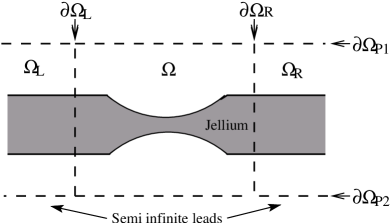
A schematic sketch of the model is in Fig. 1. It shows the region of interest between two semi-infinite leads. The potential profile is a combination of interactions between electrons and the positive constant background charge (jellium), and the external potential caused by the gate voltages. Thus, the layer of ionized donors and the 2D electron layer coincide in our model. In many models the potential profile is approximated using a harmonic potential profile [3, 21]. In our model this approximation cannot be used, because we solve for the electrostatic potential of an infinite system requiring that the system is charge neutral. In order to keep the model simple the confinement of the electrons is established by shaping the background charge and, optionally, by external potentials in certain regions of the system.
We divide the infinite system to three separate areas as shown in Fig. 1, the central area , the left region and the right region . We denote the boundary between the regions and as and between the regions and as . The Green’s functions are calculated in the region . and are non-reflecting open boundaries. On the other two boundaries, which are far enough from the important device region the potential is assumed to be infinite, so that the Green’s functions vanish there.
We solve for the self-consistent electron structure of the system iteratively. The electron density is calculated from the Green’s functions. The effective potential is calculated from the electron density as usual in the DFT within the local-density approximation (LDA). After mixing the new effective potential with potential from the previous iteration the electron density is recalculated. The loop is repeated until convergence is achieved.
The effective potential has four terms
| (1) |
where and are the Coulomb and the exchange-correlation potentials arising from the charge distributions, respectively. The calculation of is discussed below in more detail. For , we use the recent 2D-LDA functional by Attacalite et al. [22, 23].
takes care of the boundary conditions under the bias voltage [5]. The total electrostatic potential has different levels in the right and left leads. This introduces as a linear ramp potential over . In the regions and , is calculated as a potential of the infinite (jellium) wire. Then is also continuous if is large enough. The ensuing energy scheme is shown in Fig. 2. Also the Fermi levels in the right and left leads differ by the applied bias voltage . is an external gate potential. Using gate voltages it is possible to increase or decrease the potential in certain regions, for example to increase the potential walls and to decrease the potential wells of a bare jellium system.

Below we use a notation in which a point inside the two-dimensional region is denoted by and a point outside the region in region or by . A point on the boundary is and a point on is .
B Green’s functions in electronic-structure calculations
We use Green’s functions in calculating the electronic structure and the current under an external bias voltage. The theory is explained in more detail in Refs. [1] and [5]. The electron density is calculated from the Green’s function . In order to obtain one has to solve first for the retarded Green’s function from
| (2) |
where is the electron energy and is the DFT Hamiltonian the system,
| (3) |
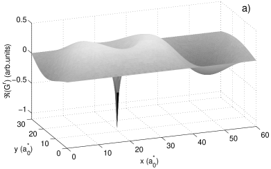
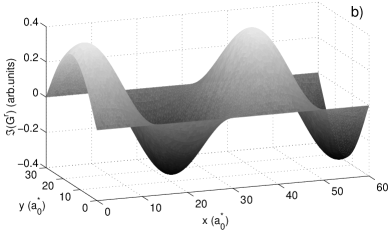
In this case is a two-dimensional variable. Its components along and perpendicular to the leads are and , respectively. is zero on the boundaries parallel to the leads (see Fig. 1). If is smaller than the bottom of the potential in the lead Eq. (2) gives exponentially decaying solutions there. Otherwise the solution oscillates with a constant amplitude to the infinity. The form of in a uniform jellium wire is shown in Fig 3. The real part has a pole at , while the imaginary part behaves smoothly everywhere. This is why the imaginary part is much easier to approximate numerically than the real part.
In equilibrium, when the Fermi functions in and are identical, , we obtain
| (4) |
This equation is also valid under a bias voltage at energies for which (in practice, for those energies). If Eq.(4) is not applicate, has to be calculated in a more complicated way. Eq. (2) can be reformulated using the so-called retarded self-energies of the leads, and , as
| (5) |
Above, is the Hamilton operator for the isolated central area . In practice, can be calculated from the boundary conditions for the Green’s functions at . are functions with non-zero values only at the boundaries . Next we define the functions as
| (6) | ||||
are the self-energies for the advanced Green’s function . One can then write the electron density as the sum of the electron flows from the leads to the region , using
| (7) | ||||
where are the Fermi functions in the right and left leads. This equation has to be used in nonequilibrium situations when .
Eq. (7) corresponds to the electron density due to the states extending to infinity in the leads. Eq. (4) includes also the electron density of possible bound states, which are localized near and decay exponentially in the leads.

In order to calculate total electron density we integrate over the electron energy
| (8) |
We use both equations (4) and (7) in this integration. Eq. (4) is analytic in the upper half of the imaginary -plane whereas Eq. (7) has poles below and above the real axis. Thus, using Eq. (4) it is possible the transfer the integral path from the real axis to the complex plane. Our integration path is shown in Fig 4. The first part is a semi-circle in the complex -plane using Eq. (4) and it takes care of the possible bound states below the energy bands of the leads. The rest of the integration, , is close to the real axis and there Eq. (7) is used. On the semi-circle only few integration points are needed because the rapid variations of are smeared out when the integration leaves the real axis. This is specially useful for the bound states, which give rise to sharp peaks near the real axis.
Computationally, it is faster to solve for from Eq. (7) than from Eq. (4). Eq. (4) results in the inversion of the entire matrix, because one needs in all the discretion points of . Electron density in Eq. (8) is the calculated using the diagonal entries of the imaginary part, . Inversion of the matrix using direct sparse routines from HSL [7] occurs as follows. First one performs the symbolic analysis and factorization to produce an ordering that reduces the fill-in. After that a numerical factorization with pivoting is performed producing the Cholesky factor of the matrix. The a set of linear equations with different right-hand sides are solved. The number of equation is equal to the dimension of the matrix. Eq. (7) needs only the Green’s functions for on the boundaries . This means that after factorization one has to solve for a set of only as many linear equations as there are discretization points on .
For 2D systems the use of Eq. (4) is justified because the analytic continuation of the integrand reduces the number of points needed in the numerical integration of Eq. (8) and because the discretization error is smaller for Eq. (4) than for Eq. (7). Namely, only the imaginary part of is used in Eq. (8) so that the pole of does not cause any major numerical problems if Eq. (4) is used.
C Electric Current
The electric current is also calculated using the Green’s functions. The electron tunneling probability through the central region is obtained from
| (9) | ||||
and the total current is calculated integrating over the energy, and taking care of the electron occupations in both leads. In the effective atomic units the result is
| (10) |
III Finite-element method for solving Green’s functions
A Variational formulation
The most demanding computational task is to find the Green’s function at different energies as presented above. To this end, we first divide the domain of the problem into two disjoint parts, the computational domain and the exterior domain . Only the computational domain is discretized whereas the exterior is taken care of by the corresponding Green’s function (see below Ch. III E). First, we cast Eq. (2) into a variational, or weak, formulation for the domain . During the derivation we frequently make use of the Green’s formula
| (11) |
for two arbitrary, sufficiently smoothly behaving functions and . Above, denotes the outward normal of , and the line integration is taken in the counter-clockwise direction around the 2D area .
To proceed, we multiply Eq. (2) by a sufficiently smooth function and integrate the resulting identity over giving
| (12) | ||||
The use of the Green’s formula of Eq. (11) gives
| (13) | ||||
Thus, the original problem of Eq. (2) is equivalent to the formulation
| (14) | ||||
for any sufficiently smooth function .
In order to obtain a solvable system, the boundary conditions must be supplied at the boundaries and . For conciseness we discuss only the case of , the other case being similar. Consider the exterior problem
| (15) | |||||
| (16) |
for the Green’s functions of the semi-infinite lead. It follows that any sufficiently smooth function can be written in the form
| (17) | ||||
for . Using the Green’s formula (11) for the exterior domain twice we can write
| (18) | ||||
so that
| (19) | ||||
We assume that is the solution to the homogeneous problem for . Since on we have by Eq. (19)
| (20) | ||||
Now the representation formula (20) can be used to supply the boundary condition to Eq. (14). Differentiating Eq. (20) with respect to and letting we obtain the term corresponding to the left boundary in Eq. (14) as
| (21) | ||||
Here we have derived the variational form for the self-energy operator . It includes line integrals over the boundary together with a trace mapping from functions on to the functions on . The function in Eq. (6) is given by
| (22) |
with zero extension outside the boundary .
The mapping generated above by Eq. (21) is called the Dirichlet-to-Neumann mapping since in general it maps the Dirichlet datum of a solution to a partial differential equation to the corresponding Neumann datum .
B Finite-element discretization
To obtain a numerical approximation for the Green’s function in the computational domain we select a finite-dimensional space defined on and project our problem of Eq. (14) into by solving for such that
| (23) | ||||
for every [28]. A matrix equation is obtained by selecting a basis for and expanding in the basis,
| (24) |
Selecting in Eq. (23) we obtain
| (25) | ||||
Denoting
| (26) | ||||
and exploiting the symmetry of the coefficients we see that ’s are the entries in the inverse of the matrix the given by Eq. (26).
We connect to the discretized forms as
| (27) |
Further, let us denote
| (28) |
and
| (29) |
with
| (30) |
since is symmetric. Now, for example, the electron tunneling probability of Eq. (9) can be written in the discretized form as
| (31) | ||||
C Finite-element basis
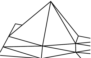
So far we have not touched the subject of selecting the basis functions in Sec. B above and thus the space . In principle, we could select any computable set , but adhere to a traditional choice in the finite-element practice, namely to the set of piecewise polynomial functions. The basis functions are constructed as follows. Assume that is partitioned into a simple mesh of nodes and polygons conforming to the usual requirements imposed on a finite-element mesh. These polygons can have a variety of shapes but the simplest choice of triangles in two (and tetrahedral in three) dimensions will serve our purposes. We choose the basis functions to be element-wise linear functions that have the value one in a single node of the mesh and zero in other nodes (see Fig. 5). The corresponding finite-element space is
| (32) | ||||
where denotes the set of continuous functions in and is the set of polynomials of degree one in the polygon .
An element-wise polynomial basis has several advantages. First, polynomials are fast to evaluate and they can be integrated exactly on a suitable reference element. Second, the piecewise nature of the functions ensures that the matrix is very sparse. Third, the accuracy of the discretization can be controlled via mesh refinements and coarsening.
The piecewise nature of the basis functions gives rise to a sparse matrix. Due to recent developments in linear algebra there are fast direct solvers[24] (also parallel)[25, 26] for sparse systems arising from discretization of partial differential equations. Since we must solve for all the coefficients of the approximate Green’s function we are faced with the problem of solving linear systems with different right-hand sides. This kind of setting is favorable to direct methods over iterative ones. Nevertheless, the computation itself is a time-consuming procedure and cannot be substantially accelerated with the techniques known today.
D Mesh generation
An important property affecting the quality of the finite-element approximation is the underlying mesh and especially the shape and the size of individual elements. Several techniques for mesh generation in two and three dimensions are available. All the techniques have in common that they try to produce meshes with elements of desired local size and high quality. There are also several indicators for evaluating the quality of the shape of a single element. Perhaps the most common is to require that there are no large angles in the element. Typically, the larger the maximal angle of an element is, the worse the resulting approximation will be.
In this work we use Delaunay meshes [27] for triangular elements in two-dimensional problems. They are known to be very robust in producing high-quality triangular meshes for different shapes of domains. A Delaunay mesh can be characterized as follows. A mesh consisting of nodes and triangular (or tetrahedral) elements satisfies the Delaunay criterion if the circumscribe of a triangle (or tetrahedron) of the mesh contains no nodes of the mesh. Meshes satisfying the Delaunay criterion are called Delaunay meshes.
It can be shown that for a given set of points in a plane a Delaunay triangulation always exists and is even unique with a minor assumption on the placement of the nodes. Furthermore, among all triangulations of the nodes, the Delaunay triangulation maximizes the minimum angle present in the triangulation. The max-min property can be usually considered as a guarantee of high-quality elements.
Unfortunately the Delaunay criterion is not sufficient for a high quality tetrahedral mesh in three dimensions. This is due to the presence of “slivers” in Delaunay meshes. These elements can have very large angles deteriorating the approximation capabilities, and yet they satisfy the Delaunay property. Therefore alternative techniques must be sought for when producing meshes in three dimensions. Typical approaches use a mixture of different methods, e.g. octree methods, advancing front methods, and Delaunay methods.
However, it should be noted that the quality of the resulting mesh produced by a mesh generation algorithm depends heavily on the shape of the domain to be meshed. Very simple domains such as cubes and other rectangular domains are usually well treated by virtually any method, whereas more complicated domains having holes and cuts need more attention.
E Exterior Green’s function
The exterior Green’s function for the semi-infinite leads can be calculated numerically as the surface Green’s function of a periodic system [14]. In the present work the potential is uniform in the leads along the lead axis. Therefore we can solve for the isolated Green’s function using the analytic one-dimensional solution along the lead and the numerical transverse wave functions [1]. The ensuing exterior Green’s function for the quasi-two-dimensional semi-infinite wire is
| (33) |
where ’s are solutions to the Kohn-Sham equation
| (34) |
with
| (35) |
We solve Eq. (34) using self-consistency iterations for the electron density and the potential profile . As explained before we use a model in which the positive charge forms a thin wire and the electron wave functions spread out of this charge. The effective potential consists only of and , and no external potential is applied. In practice the summation in Eq. (33) is truncated typically after a few tens of states so that the results are well-converged.
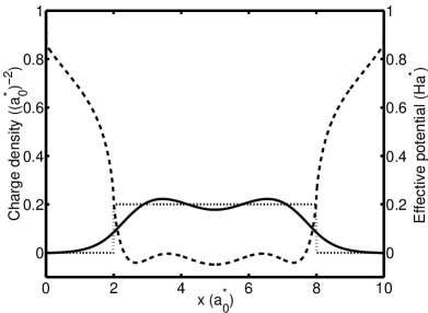
The charge densities resulting from this calculation are used in the boundary conditions when calculating the Coulomb potential of the nanosystem. The total charge per unit length is zero in an infinite wire, but there are local variations in the charge density in the transverse direction. As an example, we show in Fig. 6 the effective potential and the positive and negative charge densities in a case with two transversal modes in the wire. A cut perpendicular to the wire axis is shown.
F Coulomb interactions
The effective potential is also calculated using the FEM and the same mesh as for the Green’s functions is used. is simply evaluated in every node point. The potential charge densities are two-dimensional but the Coulomb is treated in three dimensions. In this case it is not efficient to solve for the three-dimensional Poisson equation, but to evaluate the integral
| (36) |
Above, is the electron density and is the positive background charge density. The integral is evaluated by integrating basic functions in every element. For elements with no pole ( is not inside the element), the integral is evaluated using the Gaussian quadrature rules for triangles [29]. Elements which have in one corner are evaluated by making a mapping from the triangle to a square in which the pole disappears [30].
IV Test systems
This section is devoted for testing and demonstrating our scheme. First the transmission probability over a given potential well and through a given bottle-neck potential are determined. The aim of these non-self-consistent calculations is to provide, trough the comparison with the exact results, an idea of the numerical accuracy of our methods. Thereafter we demonstrate the possibilities of the scheme by solving self-consistently the electronic structure and the current under a bias voltage for different resonant tunneling systems.
A Transmission probability over a potential well
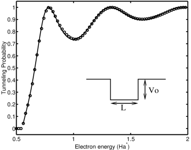
Basic quantum mechanics gives the transmission probability over a potential well (see the inset in Fig. 7) as
| (37) |
where and are the depth and the length of the well, respectively, and is the electron energy. Our numerical approach obeys this result accurately. For example, Fig. 7 gives the transmission probability calculated using Eqs. (9) and (31) for a narrow wire with a potential well. For the energies shown there is only one transverse mode in the wire. The good agreement between the numerical and analytic results indicates that the FEM mesh is fine enough.
B Transmission probability through a bottle-neck potential
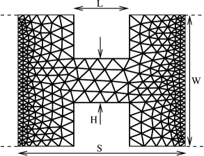
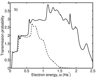
Next we study how the FEM node density affects the results. We calculate the electron transmission probability as a function of energy using different FEM meshes. Our scattering potential is a bottleneck shown in Fig. 8. The electron transmission probability is shown in Fig.9 as a function of the energy. In stepwise jumps in the transmission probability mean that new transverse modes emerg with increasing energy . The narrow peaks near the beginning of each step correspond to the constructive interference of the incident wave with the wave reflected twice at the lead-bottleneck boundaries [31]. Increasing the energy means making the electron wavelength shorter so that more points are needed to describe the wave functions. Thus, with a fixed element size it is possible to characterize transversal modes up to a certain energy only. Thereafter the transmission probability collapses due to the a loss of numerical stability.
In Fig. 9a the size of the elements in each calculation is the same throughout the whole calculation area. According to the two uppermost curves corresponding to the FEM node distances and , we need about 4 nodes between the adjacent zero-value lines of the electron wave function. This means that the FEM node distance of should give a reasonable result for the first transversal mode. In contrast, the results show large oscillations of the transmission due to discretization errors. The reason for this is that the pole of the real part of the Green’s function is not approximated accurately enough. When determining the transmission the arguments of the Green’s function are on the opposite boundaries (Eq. (9)). These Green’s function values are calculated by solving a linear equation problem in which one of the arguments of is fixed e.g. on the left boundary, and the other argument runs over the central region to the right boundary . If the FEM mesh is not dense enough near the left boundary where the pole is a large numerical error propagates to the elements needed in Eq. (9) [32]. In Fig. 9b the number of points at the boundaries is larger than inside the calculation area . The figure shows that the effects of the discretization errors are now strongly reduced at low energies, but the transmission probability at high energies collapses as fast as in Fig. 9. In conclusion, when one wants to describe the transmission probability only up to a certain energy value, the optimum way to choose the sizes of the elements is to use smaller elements near the boundaries than inside the area . In this simple test system the bottleneck potential is relative wide, but if the bottleneck is narrow in comparison with to the rest of the wire, it is reasonable to refine the mesh also in the neck region. Finally, the above refinement is also needed when calculating the electron density in nonequlibrium using Eq. (7). The real part of is needed between a point on the boundary, and an arbitrary point in the central region .
C Resonant tunneling through double-barrier potential systems
1 Symmetric barrier system
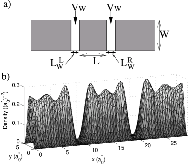
In this subsection we demonstrate the potential of our scheme by showing results of self-consistent electronic-structure calculations for 2D nanostructures under a finite bias voltage. We restrict ourselves to zero temperature calculations. The test system is a double-barrier potential structure, a schematic sketch of which is shown Fig. 10a. A jellium wire is cut by two vacuum regions and additional potential barriers are introduced within them in order to adjust the potential and the transmission. We consider two special cases. Case A has thinner potential walls than case B for which . This difference means that the connection to the leads differs remarkably its the strength. We make contact with real semiconductor systems by converting our results from the effective atomic units to the SI-units using the effective mass of electrons and the dielectric constant for GaAs. Then and . The positive background charge density corresponds to a reasonable electron density at the GaAs/AlGaAs interface. The groundstate electron density of the double-barrier system is shown in Fig. 10b, exhibiting Friedel oscillations in both leads. The wires are so thin that only one transverse mode is occupied.
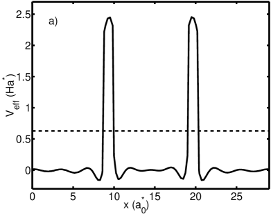
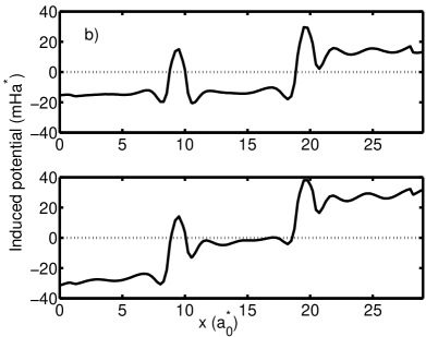
The effective potential along the symmetry axis of the double-barrier system at zero bias voltage is shown in Fig. 11a. The potential barriers are so small that the quantum dot is strongly connected to the leads. When we add the bias voltage to the system, the potential of right lead increases and that of the left lead decreases. The change of for case B is shown in Fig. 11b. The maximum bias voltage applied is small in comparison to the barrier heights. The potential drop occurs between the potential walls, not in the leads. This is expected because the leads are ballistic, with no scatterers at all. At small values the potential in the quantum dot stays at the level of the potential in the left lead. This is seen in the upper panel of Fig. 11b. When is large enough the potential in the dot rises close to the mean value in the leads (see the lower panel). A nearly inversion-symmetric potential develops. In case A the potential in the quantum dot develops differently. It follows mainly the potential level of the right lead for all bias voltages studied.
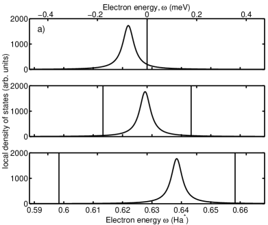
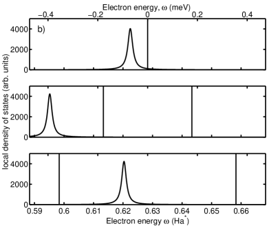
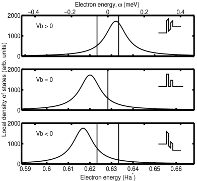
The behavior of the potential level in the quantum dot is connected to the occupation of the dot resonance state and its position relative to the lead Fermi levels. Fig. 12 shows the local density of states (LDOS) calculated by integrating over the quantum dot area. For the zero bias voltage, both cases, A and B, have a resonance peak below the Fermi level. When the bias is applied the potentials and the Fermi levels are shifted by and in the left and right leads, respectively. This defines the so-called bias window on the energy axis. At small the value the resonance peak to case B moves down in energy. The resonance, which gives a large contribution to the charge in the dot is below the left Fermi level. The bias induced charge redistribution takes place near the left barrier. Thus the potential in quantum dot stays at the level of the left lead. However, when is large enough the resonance peak enters the bias window, the charge redistribution occurs quite symmetrically at both barriers and the potential level in the quantum dot is in the middle between the left and right lead levels. The resonance peak of case A is wider than that of case B because the connection to the leads is stronger. The wide resonance enters the bias window at a low bias value and its position follows the Fermi level of the right lead. Then the bias-induced charge redistribution takes place at the left barrier and the potential level in the dot follows that in the right lead. The asymmetric behavior of the voltage drop in our model systems has analogies with the case of atomic chains between two electrodes [33]
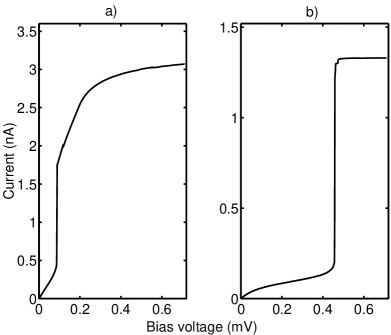
The position of the resonance peak relative to the Fermi levels has a large effect on the electron transmission probability through the double-barrier potential system. The current flow is due to the states with energies between right and left Fermi-levels i.e. in the bias window. When the resonance peak moves into this region there is a steep increase in the current. Thereafter the current stays approximately constant as a function of the bias voltage. This characteristic behavior of the double barrier potential is visible in Fig. 13. Case B with the sharper resonance peak has a steeper raise of the current than case A. Moreover, the raise occurs at a higher bias voltage in case B than in case A.
2 Asymmetric barriers
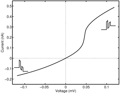
So far both the potential barriers in the system of Fig. 10a have been identical. Inspired by the prospect to use non-symmetric molecules as rectifiers [34, 35] we have studied also double-barrier systems with non-identical barriers. The zero-bias conductivities of the cases A and B (see Fig. 13 and its caption) are and . These are of the same order in magnitude as conductivities calculated for molecules between electrodes [35]. In the next example we have reduced the height of the second barrier in case A by a factor of two in order to create an asymmetric system.
The ensuing current-voltage curve is shown in Fig. 14. The curve is asymmetric with respect to the direction of the applied bias. The double-barrier system shows a clear rectification effect resembling that for asymmetric molecular wires [35]. The reason for the rectification effect is seen in the LDOS in the quantum dot given in Fig. 15. When the bias over the system is zero a resonance peak is below the Fermi level as it was in the previous cases A and B. For positive bias voltages (the potential is higher in the lower-barrier side) the resonance peak moves up in energy and the resonance is emptying of electrons. This causes the increase in the conductivity. In the case of negative bias voltages (the potential is higher in the higher-barrier side) the resonance peak follows the Fermi energy of the lower-potential lead. The situation is similar to that of system B above at low bias. The resonance does not enter the bias window as fast as in the case of the positive voltage and the current increases slowly.
V Conclusions
We have developed a computational scheme to model two-dimensional nanostructures connected to two semi-infinite leads. The electron density and the current are calculated self-consistently using the non-equilibrium Green’s function approch. The single-particle electron states are handled within the density-functional theory.
We have formulated the problem using the finite-element approximation. In this approximation the boundary conditions are easy to derive and implement. We have shown the derivation of the Dirichlet-to-Neumann boundary conditions and the discretized forms of physical quantities such as the tunneling probability.
Tests with model potential systems show the numerical accuracy and its dependence on the finite-element mesh chosen. Especially, we show that for efficient accurate calculation is important to refine the mesh near the boundaries between central region and the boundaries. Self-consistent calculations for resonant tunneling structures demonstrate the efficiency of the scheme.
We have treated systems with upto 10 000 degrees of freedom. Three-dimensional atomistic systems described by of pseudopotentials would need roughly one order of magnitude more degrees of freedom withch is wihin present-day computational capabilities. The present two-dimensional work is an important step in the development towards three-dimensional atomistic modeling of non-equilibrium transport in nanoscale devices.
ACKNOWLEDGMENTS
We thank Dr. Per Hyldgaard and Dr. Harri Hakula for many enlightening discussions.
We acknowledge the generous computer resources from the Center for Scientific Computing, Espoo, Finland. This research has been supported by the Academy of Finland through its Centers of Excellence Program (2000-2005).
REFERENCES
- [1] S. Datta, Electronic Transport in Mesoscopic Systems, Cambridge University Press (1995).
- [2] W. M. C. Foulkes, L. Mitas and R. J. Needs and G. Rajagopal, Rev. Mod. Phys. 73, 33 (2001).
- [3] S. M. Reimann and M. Manninen, Rev. Mod. Phys. 74, 1283 (2002).
- [4] N. D. Lang, Phys. Rev. B 52 5335 (1995).
- [5] Y. Xue, S. Datta and M. A. Ratner, Chemical Physics 281 151-170 (2002).
- [6] For a review, see T. Beck, Rev. Mod. Phys, 72, 1041 (2000).
- [7] The Harwell Subroutine Library, see http://www.cse.clrc.ac.uk/nag/hsl/
- [8] For a review, see T. A. Arias, Rev. Mod. Phys. 71, 267 (1999).
- [9] See, for example G. Kresse and J. Furthmüller, Phys. Rev. B 54, 11169 (1996).
- [10] J. Taylor, H. Guo and J. Wang, Phys. Rev. B 63 245407 (2001).
- [11] M. Brandbyge, J. Mozos, P. Ordejoń, J. L. Taylor and K. Stokbro, Phys. Rev. B 65, 165401 (2002).
- [12] M. B. Nardelli, J.-L. Fattebert, and J. Bernholc Phys. Rev. B 64, 245423 (2001).
- [13] P. S. Damle, A. W. Ghosh, and S. Datta, Phys. Rev. B 64, 201403(R) (2001).
- [14] K. S. Thygesen, M. V. Bollinger, and K. W. Jacobsen, Phys. Rev. B 67, 115404 (2003).
- [15] J. E. Pask, B. M. Klein, P. A. Sterne and C. Y. Fong, Computer Physics Communications 135 1-34 (2001).
- [16] J. E. Pask, B. M. Klein, C. Y. Fong and P. A. Sterne Phys. Rev. B 59, 12352 (1999).
- [17] E. Tsuchida and M. Tsukada, Phys. Rev. B 54, 7602-7605 (1996).
- [18] E. Tsuchida and M. Tsukada Phys. Rev. B 52, 5573-5578 (1995).
- [19] S. R. White, J. W. Wilkins and M. P. Teter, Phys. Rev. B 39, 5819-5833 (1989).
- [20] S. C. Brenner, L. R. Scott, The Mathematical Theory of Finite Element Methods, Second Edition, Springer (2002).
- [21] K. Hirose, F. Zhou, and N. S. Wingreen Phys. Rev. B 63, 075301 (2001).
- [22] C. Attaccalite, S. Moroni, P. Gori-Giorgi, and G. B. Bachelet, Phys. Rev. Lett. 88, 256601 (2002).
- [23] P. Gori-Giorgi, C. Attaccalite, S. Moroni, and G. B. Bachelet, Int. J. Quantum Chem. 91, 126 (2003).
- [24] J.W.H. Liu, SIAM Review, 34 82-109 (1992)
- [25] P.R. Amestoy, I.S. Duff, and J.-Y. L’Excellent, Comput. Methods in Appl. Mech. Eng., 184, 501-520 (2000)
- [26] A. Gupta, ACM Transactions on Mathematical Software, 28 (2002)
- [27] M. Bern and D. Eppstein, Computing in Euclidean Geometry, 23-90, (World Sci. Publishing, River Edge, NJ, 1992)
- [28] D. Braess, Finite Elements (Cambridge University Press, 2001)
- [29] R. Cools and P. Rabinowitz, J. Comp. Appl. Math., 48, 309 (1993).
- [30] M. G. Duffy, SIAM Journal on Numerical Analysis, 19, 1260-1262 (1982).
- [31] A. Szafer and A. D. Stone, Phys. Rev. Lett. 62, 300-303 (1989).
- [32] I. Babuska, T. Stroubolis, The Finite Element Method and its Reliability, Oxford University Press (2001).
- [33] M. Brandbyge, N. Kobayashi, M. Tsukada Phys. Rev. B 60, 17064-17070 (1999).
- [34] V. Mujica, M. A. Ratner and A. Nitzan, Cham. Phys. 281, 147-150 (2002).
- [35] J. Taylor, M. Bradbuge, and K. Stokbro, Phys. Rev. Lett. 89, 138301 (2002).