Simple model for scanning tunneling spectroscopy of noble metal surfaces with adsorbed Kondo impurities
Abstract
A simple model is introduced to describe conductance measurements between a scanning tunneling microscope (STM) tip and a noble metal surface with adsorbed transition metal atoms which display the Kondo effect. The model assumes a realistic parameterization of the potential created by the surface and a orbital for the description of the adsorbate. Fano lineshapes associated with the Kondo resonance are found to be sensitive to details of the adsorbate-substrate interaction. For instance, bringing the adsorbate closer to the surface leads to more asymmetric lineshapes while their dependence on the tip distance is weak. We find that it is important to use a realistic surface potential, to properly include the tunnelling matrix elements to the tip and to use substrate states which are orthogonal to the adsorbate and tip states. An application of our model to Co adsorbed on Cu explains the difference in the lineshapes observed between Cu(100) and Cu(111) surfaces.
I Introduction
The study of many-body phenomena in low dimensional systems is attracting a lot of attention. This has been motivated by recent advances in the construction of nanostructures and quantum dot devices. Scanning tunneling microscopy has also opened the possibility of analyzing many-body phenomena at surfaces. For instance, the Kondo effect has been detected in STM conductance measurements of noble metal surfaces with adsorbed 3d transition metal atoms.Madhavan1 ; Manoharan ; Knorr ; Nagaoka ; Li Characteristic zero bias lineshapes are observed which are reminiscent of FanoFano phenomena.
Fano lineshapes have been observed in different situations. They were first explored by Fano Fano in his studies of autoionization of doubly excited He(2s2p) resonances lying in the continuum. In the case of adsorbed atoms on a metal surface an analogous situation is found as a localized orbital is also coupled to a continuum of metallic states. As the adsorbate is magnetic, the Kondo effect can occur and, therefore, Fano lineshapes can be thought of as arising from the interference of the Kondo resonance with the continuum of metal states.Ujsaghy It is worth noting that Fano phenomena appears in STM measurements although the tip overlaps much more strongly with the surface than with the adsorbate wavefunctions (as the 3d orbitals are very localized) so that conductance measurements reflect electronic properties of the metal surface modified by the presence of the magnetic atom.
These Fano-type lineshapes differ from one adsorbate/substrate system to another, as summarized in Table 1, although some experimental trends can be extracted. For instance, the Fano parameter, , is typically either zero or positive. As can be observed from the table the lineshape associated with is a symmetric dip close to zero bias. The dependence of lineshapes may be illustrated by comparing the asymmetric dip observed for Co on Cu(100) with the symmetric dip-like shape found for Co on Cu(111). Similarly adsorbing Ti instead of Co on Au(111) leads to a strong variation of the lineshape. The situation becomes more complicated if we consider the ”middle” elements of the 3d row which do not even show appreciable features in the conductanceJamneala down to K. This raises questions about the occurrence of the Kondo effect at all for these specific adsorbates. Hence, experimental observations suggest that details associated with the adsorbate-substrate interaction may be relevant.
| Adsorbate/Surface | TK(K) | Type of lineshape | q | Ref. |
|---|---|---|---|---|
| Co/Cu(111) | 54 | nearly symmetric dip | 0.2 | [Manoharan, ; Knorr, ] |
| Co/Cu(100) | 88 | asymmetric dip | 1.1 | [Knorr, ] |
| Co/Au(111) | 75 | asymmetric dip | 0.6 | [Madhavan1, ] |
| Ti/Au(111) | 70 | asymmetric dip+peak | 1 | [Jamneala, ] |
| Ti/Ag(100) | 40 | asymmetric dip+peak | 1 | [Nagaoka, ] |
| Ce/Ag(111) | 500 | symmetric dip | 0 | [Li, ] |
| Co/Ag(111) | 92 | symmetric dip | 0 | [Schneider, ] |
The Fano parameter, , governing the shape of the conductance, , close to zero bias, is given by:
| (1) |
where reads:
| (2) |
and, , is the Kramers-Kronig transformation of :
| (3) |
In the above equations, and are the tip-substrate and adsorbate-substrate matrix elements, respectively. is the substrate band dispersion and the position of the Fermi level.
In order to understand the relation between the energy dependence of and the conductance lineshape we consider first in Fig. 1 two different situations attending to the degree of asymmetry of :

(i) is symmetric with respect to the Fermi energy. In this case, and the Fano parameter, . Hence, the resulting conductance lineshape is a symmetric dip. (ii) is asymmetric with most of its weight situated at frequencies below the Fermi energy . For this case, and conductance lineshapes are more asymmetric ( in the most asymmetric lineshape). Hence, experimental observations requires that is in between cases (i) and (ii).
However, if we consider an sp-like band for the substrate and assume that hybridization matrix elements are independent of momentum, would be parabolic (from Eq. (2)), growing up to infinite energies. Due to the large asymmetry in , would be very large and negative so that leading to a peak (see Fig. 1) rather than the dip typically observed in experiments. Hence, it seems difficult to reconcile the observed conductance lineshapes with the shape of from this simplified picture. The question that we address in the present work is whether the momentum dependence of hybridization matrix elements can change leading to more symmetric conductance lineshapes.
First attempts to model the substrate electronic structure have been carried out by Plihal and GadzukPlihal who have used a Jellium metal with a sharp step potential barrier at the surface. However, a half-filled symmetric density of states to describe the substrate (instead of parabolic) and momentum independent adsorbate-substrate hybridization matrix elements, , were used. Under these strong assumptions dip-like conductance lineshapes were obtained. Tight-binding descriptions of the substrate have also been used.Schiller They provide a qualitative understanding of observations although their use is difficult to justify considering the sp free-like bands of noble metal surfaces.
The above discussion shows the difficulty of describing experimental observations in a consistent way and points out the need of a more realistic model for describing the adsorbate-substrate-tip system.
An issue which needs to be carefully addressed in defining the relevant model is to know which of the states associated with the surface (either surface and/or bulk states) are more strongly coupled to the adsorbate. There is experimental evidence suggesting that surface states play only a minor role in the metal-adsorbate interaction Knorr . For instance, the amplitude of the conductance decays rapidly as, , with lateral displacement of the tip, , instead of decaying as expected for surface states coupled to the impurity. Furthermore, this bulk-like behavior persists in conductance measurements of Co on Cu(111), which is known to have a surface state at the Fermi energy Knorr . Based on the above experimental observations we will only consider bulk states in our model. Another experimental observation is that lineshapes depend only weakly with perpendicular tip-substrate distance, , suggesting that the direct interaction between the tip and the adsorbate is negligibleMadhavan2 .
In the present work we show how using an Anderson model in an appropriate orthogonalized basis, reasonably symmetric shapes of are found which lead to conductance lineshapes in agreement with observations. We find that the momentum dependence of the hybridization matrix elements between the adsorbate orbital and the orthogonalized metal wavefunctions together with the finite size of the tip wavefunction are responsible for this behavior.
The present paper is organized as follows. In Section II we introduce an Anderson model in an orthogonalized basis to describe the adsorbate-substrate interaction together with the relevant formulas needed for discussing STM conductance measurements. In Section III we compute the parameters involved in the adsorbate- substrate interaction needed in the Anderson model. Section IV is devoted to describing the main results of our model. Finally, in Section V, we apply the model proposed to conductance measurements of Co atoms on noble metal surfaces.
II Theoretical approach
In this section, details about the model used are given. An Anderson model on an orthogonal basis is considered. The parameters of the model are computed taking into account the following considerations: (i) Instead of a step barrier we consider a Jones-Jennings-Jepsen (JJJ) potential Jones to describe the metal surface wavefunctions, (ii) we neglect the direct coupling of the tip with the substrate d bands and with the 3d orbital of the adsorbate due to the localized nature of the d orbitals, (iii) the adsorbate is modelled by a single d-orbital, and (iv) the momentum dependence of the hybridization matrix elements is explicitly taken into account.
Metallic states, , coupled to a single orbital denoted by are considered. The Anderson model usually assumes that the cotinuum of metal states are orthogonal to the localized orbitals of the adsorbate. However, the basis set formed by the unperturbed metal, adsorbate and tip wavefunctions, , is non-orthogonal (in general) and overcomplete.
One way to take into account orthogonalization effects is to redefine the metallic states, , as:
| (4) |
Considering that tip and adsorbate wavefunctions are orthogonal: , as is very localized, then the new metallic states satisfy
| (5) |
where can be either or .
Our starting point is an Anderson model defined in this new orthogonal basis: , from which associated one-electron parameters, , and are obtained. An analogous procedure was previously used in the context of chemisorption of atoms and molecules on metal surfaces by Grimley. Grimley
It is worth mentioning that the new metallic states are non-orthogonal among each other:
| (6) |
Hence, the orthogonalization condition between different states is violated. However, this occurs at higher order in the overlap: .
II.1 Model
From the above considerations, our model for the complete tip-substrate system (with the 3d transition metal atom) reads
| (7) |
where describes the substrate with the adsorbed 3d transition metal atom and describes the interaction of the tip with the substrate. describes the tip which is assumed to have an unstructured density of states.
The substrate with the adsorbed 3d atom may be modelled by a generalized Anderson model that explicitly includes the orbital degeneracy of the 3d-orbital
| (8) | |||||
Here is the energy level of an electron residing in the orbital of the adsorbate, creates an electron with spin , momentum and perpendicular projection of angular momentum, , in the metal. creates an electron in the state with perpendicular projection of angular momentum in the adsorbate. and are the metallic energies and the hybridization matrix elements between the substrate and the adsorbate, respectively. is the Coulomb repulsion of two electrons in the 3d orbital of the transition metal atom.
We will restrict the sum to as this is the orbital which is more strongly hybridized to the metallic surface.Weissman . In this case, Hamiltonian (8) reduces to the standard Anderson impurity model containing the spin degeneracy only.
Finally, the tip-substrate interaction contribution to the Hamiltonian reads
| (9) |
through the matrix elements, . Here, destroys an electron with spin in the tip.
II.2 Hybridization matrix elements
In the following we describe how hybridization matrix elements, and , are computed. For simplicity we will first focus on how is computed, as is computed in a similar way.
Ignoring the electron-electron interaction we can re-express Hamiltonian (8) in first quantized form
| (10) |
where is the kinetic energy of the system, is the potential created by the adsorbate and describes the surface potential.
From Eqs. (4) and (10), the matrix elements between the orthogonalized metallic states, , and the adsorbate read:
| (11) |
where, again, we have assumed: .
The first term in Eq. (11) is the hybridization matrix element with the unperturbed wavefunctions :
| (12) |
and the second contains the overlap matrix element
| (13) |
The above orthogonalization procedure automatically selects the metal potential in the hybridization matrix elements favouring the region close to or inside the metal in the integrations. This differs from hybridization matrix elements computed with the original wavefunctions as in that case integrations over the whole space are involved.
Finally we note that orthogonalization effects enter the model through matrix elements only. Orthogonalization effects on the substrate band energies can be shown to be of higher order in the overlap. Hence, we will assume in the rest of the paper.
II.3 Computation of conductance
Following Ref. [Madhavan2, ] and for the sake of clarity we derive the basic equations needed for the computation of the conductance through the STM. If we neglect any modification of the substrate due to the presence of the tip (this is reasonable considering the fact that the tip is typically at about Å above the metal surface), then the conductance measured by the STM reads: Madhavan2 ; Plihal ; Schiller
| (14) |
where
| (15) |
is the conductance associated with the clean substrate (without the adsorbed 3d transition metal atom) and is the density of states of the tip.
Modifications of the tip-surface coupling induced by the presence of the adsorbate are given by
| (16) |
In Eq. (14), is the density of states of the tip. describes the electronic properties of the adsorbate immersed in the metallic continuum including the many-body effects such as the Kondo effect induced by the on-site Coulomb interaction, , inside the localized orbital. is an analytical continuation parameter.
For convenience Eq. (16) is rewritten in the following way
| (17) |
where is defined in Eq. (2) and is the Kramers-Kronig transformation of given in Eq. (3) with the matrix elements evaluated with the orthogonalized wavefunctions, . For the systems of interest here, and are real. Function embodies the information concerning the tip-substrate-adsorbate system as it depends on the tip-adsorbate separation, , the position of the adsorbate with respect to the plane of ions, , and the metal potential described by through the matrix elements, and . In the present work we analyze how and depend on these parameters.
II.4 Fano formula for conductance
For the sake of clarity we provide the Fano expression for the conductance which can be derived from Eqs. (14)-(17) (details can be found in Ref. [Ujsaghy, ]). First of all, the Green’s function of the 3d orbital is assumed to be known and to have the simple form
| (18) | |||||
The three terms appearing in Eq. (18) correspond to the singly occupied atomic d level situated at , the Kondo peak situated at and the doubly occupied level, refered to the Fermi level, . is defined as the half-width of the 3d impurity due to its hybridizaton with the metal surface: . , , and are spectral weights associated with the Kondo, the singly occupied and doubly occupied adsorbate, respectively.
Greens function given by Eq. (18) describes a magnetic impurity coupled to a metallic host in the Kondo regime. In the next section, we will give the parameters relevant to the 3d impurities in noble metals used to model .
We introduce Eq. (18) in Eq. (17) and define . For energies, and in the Kondo regime, , the following Fano expression for the conductance is obtained:
| (19) |
where and have a weak dependence on and denotes the Fano parameter given by Eq. (1). Hence, the shape of the conductance observed, , in the STM is governed by the value of the Fano parameter, . Fig. 1 explains qualitatively the relation between and conductance lineshapes.
To conclude this section, we emphasize that Fano lineshapes arising in the present model are a consequence solely of the interference between metal and adsorbate waves. No direct coupling between the tip and the 3d adsorbate is taken into account (which in any case should be very small) nor needed to explain Fano phenomena. However, we will see below that the tip has, in fact, an important influence on the final shape of (and ) through the matrix elements, .
III Discussion of parameters and modelling of the system
From previous section it becomes clear that the shape of the conductance as a function of the bias measured by the STM depends on the parameters modelling the adsorbate-substrate-tip interaction entering . Here we give details of how these parameters are obtained.
A. Surface potential and metal wavefunctions
A realistic and at the same time simple description of is attained by using a JJJ potential.Jones This potential interpolates between the image potential at long distances and the potential inside the bulk. It provides a realistic description of the surface barrier potential being particularly useful in interpreting LEED and photoemission data of noble metal surfaces.Jones ; Smith ; Jennings
The JJJ potential contains three parameters that can be obtained from fitting the potential to density functional calculations or experimental data. The surface potential is given (in Rydberg energy units) by:
| (20) |
Here is the depth of the bulk potential and controls the sharpness of the surface barrier potential. The parameters and are obtained by imposing the condition of continuity of the potential at (see Ref. [Jones, ] for more details). Throughout the paper we refer the tip, , the adsorbate position, , and the image plane position, , to the last plane of ions situated at (see Fig. 2) and all energies are referred to the vacuum level. The sharpness of the potential barrier experienced by the electrons inside the metal is controlled by . For increasing , for instance, the potential becomes gradually sharper. As we will see below parameter turns out to play an important role in our model.
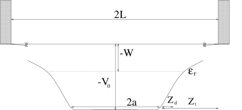
Metallic wavefunctions are obtained considering box quantization. We define a large box of side , which describes the substrate enclosed by a larger box of side , where the relative sizes of the boxes satisfy: (see Fig. 2). In practice it is sufficient to take . The perpendicular dependence of the wavefunction is obtained from the integration of Schrödingers equation in the presence of the JJJ potential starting at distances of about Å outside the surface towards the metal. Imposing periodic boundary conditions in the parallel direction, the crystal wavefunction reads:
| (21) |
where, , is the perpendicular part of the full wavefunction. Sates above the vacuum are normalized to the volume while states below it are normalized to .
B. Tip and adsorbate wavefunctions
The adsorbate wavefunction is described using a Slater-type function:
| (22) |
where is the main quantum number, the angular momentum and the z-component of the angular momentum. The normalization constant of orbital is and is a conventional spherical harmonic. For the 3d transition metal atom we use with an exponential decay , where is the Bohr radius.
Following Tersoff and Hamann,Tersoff the tip wavefunction, , is described by a simple s-type orbital (), with an exponential decay fixed by the workfunction of the metal surface: , where is the electron mass and is the workfunction of the metal surface which we take to be eV in our calculations. This choice for relies on the fact that, typically, tungsten tips are dipped in the metal surface before measuring the conductance between the STM tip and the surface.Schneider Hence, it is reasonable to describe the wavefunction tails sticking out from the tip with the same exponential decay as the ones describing the metal surface.
C. Computation of matrix elements
Once we have obtained the wavefunctions of the substrate we may proceed with the computation of the hybridization and overlap matrix elements defined in Eq. (11). For simplicity we discuss the adsorbate-substrate hybridization matrix elements. From Eq. (21) hybridization and overlap matrix elements expressed in cylindrical coordinates, read:
| (23) |
where is the cylindrical Bessel function of zeroth order, , is the surface potential and is the adsorbate wavefunction. The computation of the tip-substrate hybridization matrix elements, , proceeds along similar lines replacing by .
The behavior of tip matrix elements deserves careful attention. Due to the slow decay of the tip wave function, most of the contribution to comes from the region close to the metal surface for not too large. Matrix elements can then be approximately factorized asPlihal :
| (24) |
where is independent of the tip position. This remains true for Å-1, which is close to Å-1 (for eV). The function is related to the value of the tip wave function in the surface region and it decays rapidlymatrixtip with . is found to have a weak dependence on in contrast to matrix elements obtained from the original substrate wavefunctions as can be observed in Fig. 3. Indeed, using in the matrix elements as imposed by the orthogonalization cuts off part of the exponential dependence of metal wavefunctions far from the surface leading to a weaker dependence on . This is crucial to obtain reasonable shapes of .
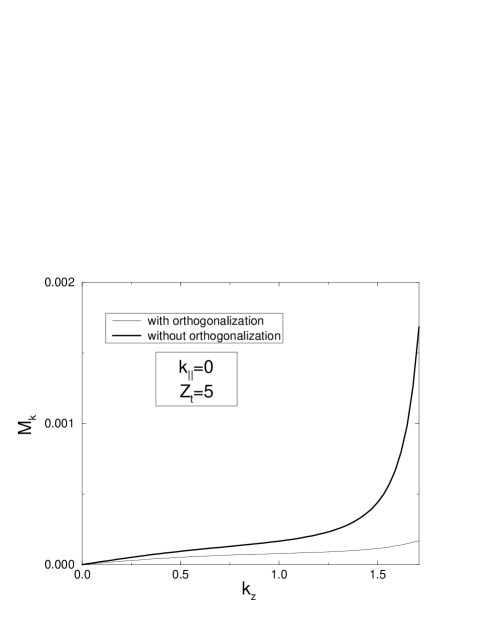
In order to have a qualitative understanding of the behavior of adsorbate-substrate hybridization matrix elements, , we focus on electrons which have no parallel momentum, . Matrix elements gradually increase with increasing due to increasing overlap of the metal states with the adsorbate. The behavior of matrix elements at large can be partially understood by analyzing Eq. (23) with nearly constant, (which is the case for the metal wavefunction outside the surface). For a adsorbate the associated matrix elements, would tend to zero due to cancellations associated with the lobes of the 3d-orbital. Indeed, we find that while computed for a d-orbital presents a downturn at intermediate Å-1, computed with an s-type orbital increases rapidly up to . Orthogonalization effects are also important as can be noticed from the fact that as . Hence, we find that matrix elements computed using orthogonalized wavefunctions, , initially increase with , reach a maximum and then they are gradually suppressed regardless of the angular dependence of the adsorbate orbital. This dependence of is reflected in the frequency dependence of . The above discussion illustrates the importance of appropriately including orthogonalization effects in the computation of hybridization matrix elements.
The behavior of matrix elements at very large perpendicular momentum needs to be carefully examined. Metallic waves with large momentum (corresponding to energies far above the vacuum level), contain rapid oscillations which lead to cancellations in the integrand of Eq. (23). A high energy cut-off may be simply estimated from: . This gives eV for the adsorbate and eV for the tip. Hence, hybridization matrix elements and in turn will be non-zero in the energy range . It is remarkable that the tip cuts off all high energy contributions having an important influence on the final shape of and in turn on conductance lineshapes. This point seems to have been overlooked before.
D. Computation of
Once we have the hybridization matrix elements, it is straightforward, following Ref. [Plihal, ] to obtain the energy dependence of given in Eq. (2). After performing integration in parallel momentum, can be written as
| (25) |
where and and is the volume. Note the factor appearing in front of the integral cancels out the volume coming from the normalization of the surface wavefunctions coming in the matrix elements.
E. Parametrization of adsorbate Greens function
In order to compute the modification induced by the adsorbate on conductance lineshapes, , knowledge of is needed. We take parameters used by Ujsaghy et. al. Ujsaghy to model Co on Au: meV, eV, eV, , and with the Kondo temperature fixed at meV. As we are particularly interested in what is happening close to the Fermi energy (at energy scales of the order of ) the relevant parameters to our calculations are and . Hence, these are input parameters which could be obtained from other sources such as experimental data or ab initio density functional calculations. It is not the purpose of the present work to have a first-principles determination of Kondo temperatures for different adsorbate/substrate systems but rather to have a qualitative understanding of conductance lineshapes.
IV Discussion of results
In this section we show our main results and discuss their relevance to experiments. A positive Fano parameter is typically found in our calculations for parameters charaterizing the noble metal surface, the adsorbate and their mutual interaction. We explore how lineshapes depend on the parameters characterizing the atom-surface interaction. These parameters are: the position of the tip , the adsorbate-substrate distance, , and the shape of the surface potential controlled by . As there is cylindrical symmetry in our model, our results only depend on the absolute magnitude of the tip-adsorbate lateral displacement . We do not find much dependence of our results with the workfunction or the height of the surface barrier so we fix eV and the workfunction eV, which are typical values for noble metal surfaces. We will first discuss the dependence of lineshapes with the tip fixed on top of the adsorbate, at a distance of about Å. At the end of the section we will study how lineshapes depend on and .
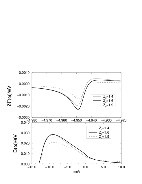
IV.1 Dependence of Fano lineshapes with adsorbate-surface distance
Fixing the tip at (on top of the adsorbate) and Å we analyze how lineshapes depend on the adsorbtion distance, . In Fig. 4 the dependence of and is shown for typical parameters describing noble metal surfaces: Å-1, eV at typical adsorbate-surface distances: Å. Adsorbtion distances for different surfaces are obtained assuming hard spheres for the atoms. At large adsorbtion distances, Å, is found to be rather symmetric with respect to the Fermi energy and consequently (see Fig. 2) the lineshape is a nearly symmetric dip. As the adsorbate is moved closer to the surface ( decreasing) the frequency dependence of varies and consequently the lineshapes too. An enhancement of weight below the Fermi energy as well as a sharper drop above it occurs. This leads to a variation of lineshapes from at large distances towards at short adsorbate-surface distances.
To understand these results, we notice that substrate states with low energy have a strong exponential decay outside the surface. As the adsorbate is brought closer to the surface, the overlap of the adsorbate orbital with these states increases. This leads to an increase of at small . States with a larger energy extend farther outside the surface and have a substantial overlap with the different lobes of the adsorbate -orbital. This tends to lead to a cancellation of the different contributions to . This tendency increases as the adsorbate is brought closer to the surface, explaining the reduction of at larger .
For comparison we also show in Fig. 5 the dependence of lineshapes with the adsorbate-surface distance for a Jellium with a step potential. Lineshapes are found to be somewhat asymmetric as a large part of the weight in situated at low energies in (see also Fig. 1). A weaker dependence of with the adsorbate-surface distance is obtained as compared to the JJJ potential. The fact that we obtain reasonable lineshapes with a simple model such as a Jellium with a step potential can be attributed to orthogonalization effects. Tip-substrate matrix elements computed without orthogonalization corrections would increase rapidly with as they involve integrations over the whole space (instead of the region close to the surface) leading to rather asymmetric shapes of .

IV.2 Dependence of lineshapes with the shape of the potential barrier
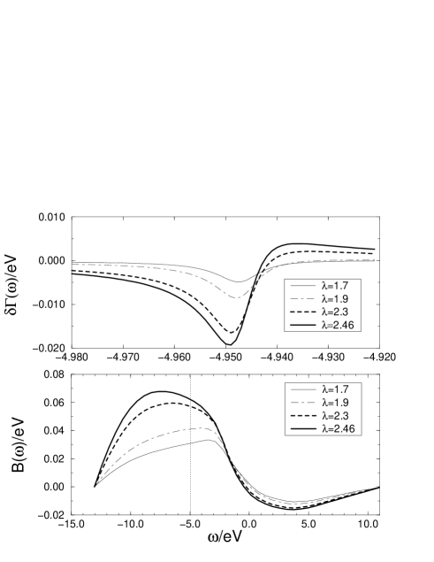
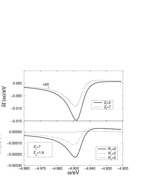
There are two parameters that can be tuned to change the shape of the surface potential. One is the image plane position, , and the other is the sharpness of the surface potential given by . We fix Å and study the dependence of and lineshapes , with the sharpness of the potential barrier. This dependence is shown in Fig. 6. We find that an increase in leads to a more asymmetric and the associated conductance lineshape, with more positive values of the Fano parameter, .
Increasing makes the metal potential, , sharper so that the exponential tails of the metal wavefunctions outside the surface are shifted closer to the adsorbate leading to a stronger metal-adsorbate overlap. This is analogous to bringing the adsorbate closer to the surface for a fixed as discussed previously. Hence, an increase in leads to an increase in the weight of at low energies and a sharper drop at energies above the Fermi level. The stronger dependence found for with than with the adsorbate-substrate distance can be ascribed to the exponential dependence of with .
Summarizing, we find that lineshapes are strongly dependent on the degree of sharpness of the metal potential. Making the surface potential sharper leads to more asymmetric lineshapes at typical atom-substrate adsorption distances.
IV.3 Dependence of conductance lineshapes with tip position
We finally discuss the dependence of conductance lineshapes when the tip is moved away from the adsorbate either laterally () or perpendicularly. The tip position comes into our calculations through matrix elements, . A weak dependence of lineshapes with perpendicular tip-substrate distance, is found. Varying the distance from 5 to 7 Å leads to a small change in the lineshape becoming slightly more asymmetric (see Fig. 7). The weak dependence of the line shape on the tip-surface distance can be understood from Eq. (24). This equation predicts a strong reduction of the amplitude of the conductance with vertical displacement of the tip , but no change in its shape. The weak dependence found is consistent with experimental observations which also indicate that the direct tip-adsorbate coupling is very small (as expected from the localized nature of the d-orbital of the adsorbate).
We can also analyze how lineshapes depend on the lateral position of the tip, . An example is shown in Fig. 7 which a rapid decay of the amplitude of the lineshapes is found. Lineshapes are found to depend slightly on at tip-surface distances of about Å which is the typical experimental tip position. Indeed, crystal wavefunctions with have the largest amplitude outside the surface representing electrons which have the largest probability of being detected by the tip (see Ref. [Plihal, ] for discussion). Hence, the oscillatory behavior appearing in Eq. (24) is suppressed as only the states with small contribute to the momentum sums.
The rapid decay of the amplitude with obtained from our calculations is consistent with the disappearance of the features in the conductance at distances of about Å. However, the small variation of the shape of the conductance with found is only partially consistent with experiments as for some systems such as Co on Cu(100) or Co on Au(111) lineshapes become gradually more symmetric () at larger . It is worth mentioning that in the case of Co on Au(111), the lateral dependence of lineshapes depends not only on the modulus of but also on the direction in which the tip is moved Madhavan1 from the adsorbate. This cannot be described in the present framework as the surface corrugation is not included in our model.
The finite size of the tip leads to a suppression of the tip-substrate matrix elements at large energies due to rapid oscillations of the metal wavefunctions providing a high energy cut-off. This cut-off turns out to be crucial to obtain reasonable lineshapes. Had we used a point-like tip the amplitude of at energies below the vacuum level would be exponentially suppressed while above it large oscillations would occur. This is because wavefunctions are evaluated far from the surface (at the tip position). Hence, for a point-like tip the Fano parameter would be very large () and a peak rather than a dip would appear in conductance measurements.
V An application to conductance measurements of Cobalt on Copper surfaces
In the previous sections a detailed description of the method used has been provided. In the following we provide the reader with an application to conductance measurements of Cu surfaces with Co atoms deposited on them.
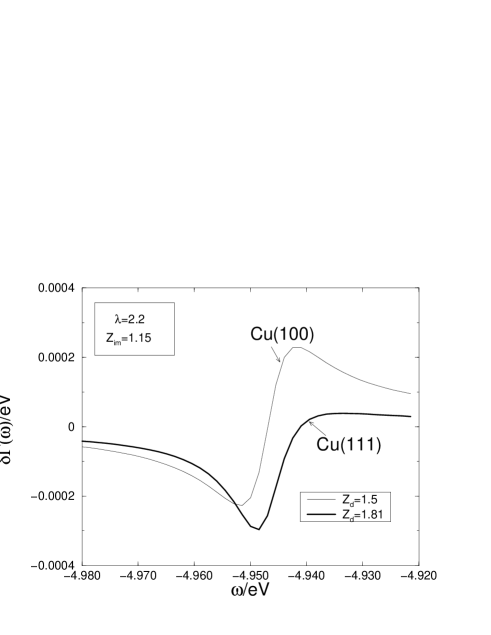
Copper surfaces are described using the parameters quoted in Ref. [Smith, ] for the analysis of surface states in noble metal surfaces. For Cu surfaces we take Å-1 and the adsorbate -substrate distance is estimated assuming hard spheres for the atoms.Pauling As the (111) surface is more closely packed than the (100) surface the Co atom adsorbs at larger distances in the former than in the latter surface. This leads to Å and Å for the (100) and (111) surfaces, respectively. At the temperatures used in the experimental studies of the conductance,Knorr Co sits outside the Cu(100) surface and it is not incorporated in the surface, as happens at higher temperatures Levanov . Ab initio calculations Scheffler then give Å, in agreement with our simple estimate. We find that difference in the adsorbtion distance is enough to produce changes in the lineshapes as can be observed in Fig. 8. From the dependence of lineshapes with discussed above we find that for Co on Cu(100) surfaces lineshapes would be more asymmetric than for Co on Cu(111). This is consistent with experiments performed for these two different surfaces.Knorr ; LNJ Our result may be of more general validity and may apply to conductance measurements on other metal surfaces such as Ag or Au. However, care should be taken as our model contains the adsorbate-substrate distance only: corrugation effects may also be important. More experiments that systematically analyze the dependence of lineshapes for Co on different crystal faces are needed to corroborate our findings.
VI Conclusions
We have introduced an Anderson model in an appropriate orthogonalized basis to analyze STM measurements of noble metal surfaces with adsorbed transition metal atoms. A realistic surface potential (JJJ potential), a single adsorbate orbital and a s-tip orbital are used to compute the parameters of the model. For typical values of the parameters characterizing the adsorbate-substrate interaction, we find lineshapes with Fano parameters, , in agreement with experimental trends.
We have introduced a function which describes the adsorbate-substrate interaction. The description of experimental observations requires a which is fairly symmetric with respect to the Fermi energy. Since the underlying density of states is approximately parabolic and the matrix elements tend to further reduce at small , it is interesting that the model, nevertheless, gives reasonable shapes for . We find that the tip matrix elements play an important role. The tip wave function is rather extended, and matrix elements to continuum states at high energies are very small, due to the rapid oscillations of the continuum states over the spatial range of the tip wave function. This helps to make more symmetric around . We also find that it is essential to use substrate states which have been orthogonalized to the adsorbate and the tip. Even when the realistic JJJ potential is used, lineshapes are found to strongly depend on the sharpness of the surface potential controlled by becoming more asymmetric with increasing (i. e. for sharper potentials). To a lower degree conductance lineshapes are also found to depend on the adsorbtion distance: the closer to the surface the adsorbate is the more asymmetric the lineshapes become. These tendencies can be explained from the enhancement in the coupling of the metal wavefunctions and the adsorbate at low energies together with the suppression at energies above the Fermi level induced by the angular dependence of the orbital and the orthogonalization.
More closely packed surfaces such as Cu(111) are expected to lead to more symmetric lineshapes than the more open Cu(100) faces as Co adsorbs further out in the former than in the latter. We find good agreement with experiments comparing lineshapes of Co on Cu(100) with Co on Cu(111) surfaces. In agreement with experiments we also find that the tip-substrate distance does not strongly influence the shape of the conductance.
Acknowledgements.
We acknowledge helpful discussions about experiments with M. A. Schneider and P. Wahl and for pointing out to us several references. J. M. was supported by a Marie Curie Fellowship of the European Community program ”Improving Human Potential” under contract No. HPMF-CT-2000-00870.References
- (1) V. Madhavan, W. Chen, T. Jamneala, M. F. Crommie, N. S. Wingreen, Science 280, 567 (1998).
- (2) H. C. Manoharan, C. P. Lutz, and D. M. Eigler, Nature 403 512 (2000).
- (3) N. Knorr, M. A. Schneider, L. Diekhöner, P. Wahl, and K. Kern, Phys. Rev. Lett. 88, 096804 (2002).
- (4) K. Nagaoka, T. Jamneala, M. Grobis, and M. F. Crommie, Phys. Rev. Lett. 88 077205 (2002).
- (5) J. Li, W-D Schneider, R. Berndt, and B. Delley, Phys. Rev. Lett. 80 2893 (1998).
- (6) U. Fano, Phys. Rev. 124, 1866 (1961).
- (7) O. Újsághy, J. Kroha, L. Szunyogh, and A. Zawadowski, Phys. Rev. Lett. 85 2557 (2000).
- (8) T. Jamneala, V. Madhavan, W. Chen, and M. F. Crommie, Phys. Rev. B 61 9990 (2000).
- (9) M. A. Schneider, L. Vitali, N. Knorr, and K. Kern, Phys. Rev. B 65 121406 (2003).
- (10) M. Plihal and J. Gadzuk, Phys. Rev. B 63, 085404 (2001).
- (11) A. Schiller and S. Hershfield, Phys. Rev. B 61, 9036 (2000).
- (12) V. Madhavan, W. Chen, T. Jamneala, M. F. Crommie, and N. S. Wingreen, Phys. Rev. B 64 165412 (2001).
- (13) R. O. Jones, P. J. Jennings, and O. Jepsen, Phys. Rev. B 29 6474 (1984).
- (14) T. B. Grimley, Molecular processes on Solid Surfaces, edited by E. Drauglis, R. D. Gretz, and R. I. Jaffee (McGraw-Hill, New York, 1969), p. 299; T. B. Grimley, Electronic Structure and Reactivity of Metal Surfaces, edited by E. G. Derouane and A. A. Lucas (Plenum Press, New York, 1976), p. 113.
- (15) M. Weissmann and A. M. Llois, Phys. Rev. B 63 113402 (2001).
- (16) P. J. Jennings, R. O. Jones, and M. Weinert, Phys. Rev. B 37 6113 (1988).
- (17) N. V. Smith, C. T. Chen, and M. Weinert, Phys. Rev. B 40 7565 (1989).
- (18) J. Tersoff and D. R. Hamann, Phys. Rev. B 31 805 (1985).
- (19) The decay is, however, somewhat slower than the exponential dependence: . This is because the tip wave function can be written as , valid for and . The second factor in this expression increases with , leading to a somewhat slower decay of than .
- (20) L. Pauling, The Chemical Bond, Cornell University Press (Cornell, 1967).
- (21) N. A. Levanov, et. al., Phys. Rev. B 61, 2230 (2000).
- (22) R. Pantecheva and M. Scheffler, Phys. Rev. B 65, 155418 (2002).
- (23) As this paper was in the finishing stage, a preprint by Lin, Castro-Neto and Jones (LCJ) Lin appeared, which addresses similar problems as the present paper. One difference between the two approaches is that non-orthogonality between the substrate, adsorbate and tip orbitals has been neglected in LCJ as is typically done in related works using the Anderson hamiltonian. However, we find that orthogonalization has important effects on tip matrix elements as shown in Fig. 3. By including orthogonalized substrate orbitals we find that lineshapes at and their dependence with the tip position are in good agreement with experimental observations unlike in LCJ who have to introduce an energy cut-off of 0.25 eV above the Fermi energy in order to explain the lineshapes of Co on Cu(100). On the other hand for the case of Co on Cu(111) LCJ have included both bulk and surface states in their calculations while we consider bulk states only.
- (24) C. Y. Lin, A. H. Castro Neto, and B. A. Jones, cond-mat/0307185.