Elecromagnetic generation and detection of dc/ac spin current
Abstract
It is shown that in a heterostructure where screening is eliminated, the Ampére-Maxwell law of electrodynamics implies that a dc or ac spinomotive force can be inudced with a time rate of change of a transverse electric field, and the magnetic analog of Ampére law implies that a dc or ac spin current can generate a transverse electric field at the same frequency outside the spin-current channel. Both effects are quite weak but may be of some usefulness.
pacs:
PACS numbers: 85.75.-d,72.25.Pn,72.25.Ba,72.25.DcThe term “spintronics” has appeared in sicentific literature for almost a decade. [2] It is broadly defined to mean any electronic application where the spin degree of freedom of an electron is non-trivially utilized. [3] The word, however, suggests another narrower definition, i.e., electronics with the electron charge replaced by the electron spin. In this narrower definition, an electric current is replaced by a spin current, which means that the spin-up and -down electrons are moving in opposite directions. (The direction of a spin current is then that of the spin-up electrons. In a non-spin-polarized conductor such a spin current is not accompanied by a net charge current.) At the same time, an electromotive force (emf) is replaced by a spinomotive force (smf), which pushes spin-up and -down electrons in opposite directions with the same force magnitude. (The direction of an smf is then that of the forces acting on the spin-up electrons.) One may also define such terms as spinoresistance, and, for an ac spin current, spinocapacitance and spinoinductance, and even entertain such notions as spinotransformer, spinorectifier, spinotransistor, etc. Will this whole line of thoughts [4] be as practically useful as electronics? An important prerequesite for an yes answer is to have a convenient power source for spin current, i.e., a device to generate an smf. Recently, the idea of a “spin-cell” has been introduced, [5] which has to some extend achieved such a goal. However, in electronics, by far the most convenient way to provide an emf is through induction — i.e., via Faraday’s law, . It has the additional advantage of allowing either a dc or an ac emf to be generated. One purpose of this letter is to show that there is indeed an inductive way to generate an smf, but not by Faraday’s law, but rather by its magnetic analog:
| (1) |
or the Ampére-Maxwell law (with the current term enclosed in brackets not important here). [6] Unfortunately, as we shall see, this process can only generate a very weak smf, although probably sufficient for some purposes. A second purpose of this letter is to show how the magnetic analog of the Biot-Savart law, or equivalently, that of Ampére’s law,
| (2) |
allows a simple electromagnetic detection of a (dc or ac) spin current, but the sensitivity is quite low, so only very large spin currents can be detected this way. Still, we think that this second idea can also have some usefulness, since observing this effect would be a solid confirmation of the existence of a spin current.
If electrons had only spin property but no charge property (like neutrons), the inductive way to generate an smf and the electromagnetic way to detect a spin current would be already contained in a paper published by the author a long time ago. [7] (That work was presented in the context of superfluid 3He-, so it can hardly reach the spintronics community. The magnitudes examined there were even smaller, due to the involvement of 3He nuclear magnetic moment, rather than the electronic magnetic moment involved here, and the very small superfluid fraction , because the phase of superfluid 3He exists in a narrow temperature range near only.) The fact that electrons also have charge property requires a modification of the idea presented there. More specifically, it is the necessity to solve the problem that an external electric field applied to a conductor is screened, and cannot reach most of the electrons in a conductor. This problem may be simply solved by fabricating a heterostructure, which is made of alternating layers of conductors and insulators, as is schematically illustrated in Fig. 1.
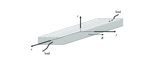
The thicknesses of these layers do not have to be strictly uniform, and the interfaces need only be reasonably flat (just to reduce surface scattering). Each conducting layer needs only to be well connected and thinner than the screening length — hence it may be necessary to use conductors with low carrier concentrations so that the screening length can encompass several atomic layers. Each insulating layer also needs to be so thick as to prohibit tunneling between the neighboring conducting layers, but not too thick in order to allow many conducting layers to be packed into a convenient size. In this way screening can be essentially suppressed for electric field applied perpendicular to the layers. The total number of conducting layers must be such that their total thickness is macroscopic, so that the device can drive a macroscopic spin current. Each conducting layer can be taken as a rectanglular sheet, as shown in Fig. 1, where the edges of these sheets are parallel to the ans axes. The end faces of this heterostructure must still be coated with a thin layer of conducting material — the two rectangular conducting sheets at in Fig. 1, so that one lead connected to one end face can send spin current into all conducting layers in the heterostructure, and another lead connected to the other end face can take spin current out of them. The leads then serve as the two terminals of this “spinovoltage generator”. [8]
To generate a dc smf across these two terminals, one must subject this heterostructure to a uniform constant time rate of change of electric field in the direction, i.e., perpendicular to the conducting sheets in the heterostructure. Let the spin-up(down) electron density in the conducting sheets be denoted as () (defined with respect to the axis). Then the spin-up electrons contribute a magnetization in the conducting sheets (in the direction), and the spin-down electrons contribute a magnetization in the conducting sheets, where is the Bohr magneton. Assuming that the electron densities are uniform in the conducting sheets, () is equivalent to a surface magnetic-charge density () at , and another surface magnetic-charge density () at . If the system is unpolarized, these magnetic charge densities exactly cancel each other. But that does not prevent opposite magnetic charges from moving in opposite directions if they are subject to a magnetic field. This magnetic field is induced by the applied according to the Ampére-Maxwell law (Eq. 1) and is at where we have neglected the dielectric property of the conducting sheets. The forces acting on all magnetic charges at due to spin-up (or down) electrons are then in the same direction, and have the magnitude This leads to a volume force acting on all spin-up (down) electrons uniformly in () directions (if ), and is therefore an smf. We propose to artificially measure it in terms of the familiar unit, volt (V) (which actually means to measure the potential energy gain per electron in V). Then the smf induced in this device (in the direction) is
| (3) |
One can also generate an ac smf this way, if one replaces the constant by the time rate of change of an ac electric field in the direction: . Then one has
| (4) |
To estimate the magnitude of this ac smf, one needs to use . This must still be multiplied by the magnetic permeability of vacuum, , before it should be used in Eq. 4, since a magnetic dipole moment appears in such formulas as (energy) , and (torque) , which contains rather than , so it does not yet have the unit of magnetic charge times length until it is multiplied by , as a magnetic charge should appear in the formula (force) , with appearing rather than . [9] Knowing that the effect is very weak, we insert in our estimate rather large but presumably still achievable values of , and viz., cm, V/m, and Hz, just to see what is the largest possible magnitude we can obtain. We then obtain the magnitude of the induced ac smf to be about V. This is still very small, but probably already sufficient for some purposes. One could still connect many such devices in series in order to get a larger smf (by another factor of 10 or even 100). Thus one could conceivably generate a several-milli-volt smf through such an inductive process. Since the frequency used already corresponds to a wave length of about 2 mm, we need to limit to be below about 1 mm, so that the electric field experienced by all electrons in the conducting sheets can be in phase. The length has no limitations except that it should not be too big, so it can be, say, 10 cm. The heterostructure should then be in a microwave cavity designed so that the (standing) wave vector is in the direction. (The wave vector should not be in the direction since the so-generated smf is proportional to , so we need to be as large as possible.) One could in principle also rotate the heterostruction in a constant electric field to get the electrons to see an ac field, but one can hardly rotate the device at Hz, so this alternative approach is impractical.
The design shown in Fig. 1, with slight modification, can also serve as a detector of a dc or ac spin current, but we shall see that the sensitivity is quite low, so only very large spin currents can be detected this way. One needs only remove the applied electric field to the device, and send the spin current through the heterostructure via the two terminals, and then detect an electric field in the direction that is generated by the spin current outside the spin-current channel. The relevant law involved is now the magnetic analog of the Ampére law, Eq. 2. As we have already explained, the magnetization due to all spin-up (or -down) electrons in a conducting sheet is equivalent to a distribution of magnetic charges of opposite signs on the two end faces at . Thus the motion of these electrons implies opposite magnetic charge currents at . Together, they may be viewed as a ring magnetic charge current in the plane which can generate an electric field in the direction. Looking at the conducting sheets from the ring magnetic charge current on each conducting sheet is clockwise from both spin-up and -down electrons (since they are moving in opposite directions), for a spin current in the direction. Thus they both generate electric field in the direction. (Notice the minus sign on the right hand side of Eq. 2.) Since each conducting sheet is very thin, the ring magnetic charge current in it may be treated as a line current. Then It is easy to work out the magnetude of the electric field generated along the axis:
| (5) |
where and (asummed ) are the thicknesses of each conducting and insulating sheet, respectively, and (, ) denote the velocities of the spin-(up,down) electrons, respectively. We have also assumed that there are conducting sheets symmetrically placed between and . Since is still very small, we can approximate the above sum by an integral. It gives
| (7) | |||||
For A/m2, and , we calculate the front factor to be V/m. This is a weak but observable electric field, but the very large spin current used in this calculation can hardly be generated by the induction method discussed above. However, in a strongly polarized or half metallic ferromagnetic metal, a very large polarized current can be generated with an ordinary emf. If such a current is sent through the present device, a detectible electric field should be generated as shown here, besides the magnetic field which must also occur because a spin-polarized current is still a charge current. Observing this electric field would then be a definitive way to confirm the existence of a spin-polarized current.
Integrating the above electric field along the whole axis, we find the total voltage drop along this axis to be:
| (8) |
For the same spin current and considered in the previous paragraph, and let cm, we obtain V, which is a detectible voltage difference, but it is cetainly a very weak one. If the spin current is ac, then the induced electric field is also ac at the same frequency. One can then possibly use a resonance technique to detect this electric field with an improved sensitivity.
We conclude this work with some remarks: (1) The conducting sheets can not be made of singlet superconductors, since if the spin-up electrons and spin-down electrons form bound Cooper pairs then they can not flow in opposite directions. p-wave superconductors do not have this problem, and it has the advantage of contributing no internal spinoresistance, so it has the potential of generating larger spin current, but one needs to worry about suppressed order parameter in sheets much thinner than their coherence length. So low-carrier-density normal conductors with low resistance and low magnetic and spin-orbit scattering centers are still the best bet for making this device. (2) spinoresistance can result from both scattering (which reduces electrons’ forward momentum) and spin conversion. So in most good conductors it should be of the same order of magnitude as its usual resistance unless the conductor has a lot of magnetic and/or spin-orbit scattering centers, in which case its spinoresistance should be larger than its usual resistance. (3) If the spin-up and -down currents can be separated in a short section of the spin circuit using half-metallic conductors, and the usual capacitors, inductors, transformers, rectifiers, or transistors, etc., are inserted in the two separate circuit branches, one would have created a spinocapacitor, a spinoinductor, a spinotransformer, a spinorectifier, or a spinotransistor, etc., but it doesn’t appear that they can allow spin circuits to maintain their advantages over the usual charge circuits. Thus more clever ideas are needed before spin circuits can compete with the usual charge circuits for usefulness.
The author wishes to thank his colleague, Joe Ross, for useful discussions. This work was supported by the Texas Center for Superconductivity and Advanced Materials at the University of Houston.
REFERENCES
- [1] Email address: crhu@tamu.edu
- [2] S. A. Wolf and D. M. Treger, Proc. IEEE 91, 650 (2003).
- [3] For recent reviews of this research area, see S. A. Wolf et al., Science 294, 1488 (2001); H. Akinaga and H. Ohno, Trans. Nanotech. 1, 19 (2002); and all articles in the special issue of Proc. IEEE cited in Ref. 1. See also, S. Das Sarma, Nature Materials 2, 292 (2003). L. P. Rokhinson et al., Microelec. Eng. 63, 147 (2002); J. De Boeck et al., Thin Solid Films 412, 3 (2002); J. Fabian and S. Das Sarma, Phys. REv. B 66, 024436 (2002); P. MavroPoulos, O. Wunnicke, and P. H. Dederichs, Phys. REv. B 66, 024416 (2002).
- [4] We suggest calling this whole line of thoughts “orthospintronics”, and referring to all other spintronic ideas and applications as “paraspintronics”.
- [5] Q.-F. Sun, H. Guo, and J. Wang, Phys. Rev. Lett. 90, 258301 (2003).
- [6] If magnetic charge exists, this law allows the generation of a magnetomotive force to drive a magnetic charge current. (This term has been used in another sense which is really a misnomer [cf., for example, Sear, Zemansky, and Young, University Physics, part II, 5th ed., Addison-Wesley, 1976, pp. 604].) Here we show that the same law can also lead to an smf.
- [7] C.-R. Hu, Phys. Rev. Lett. 82, 1493 (1982).
- [8] This heterostructure may be also fabricated as a semiconductor multi-quantum-well structure. However, in order for the device to work at room temperatures, a very wide gap semiconductor must be used as the material between the quantum wells. The quantum wells must also be doped to serve as the conducting sheets. Their electron density can be controlled to ensure that the width of the quantum wells are less than the screening length.
- [9] See, for example, J. D. Jackson, Classical Electrodynamics, 3rd Ed. (John Wiley and Sons, Inc., New York, 1999), Eqs. (5.1), (5.72), and (6.150). The units of and can be obtained through these equations.