Combined atomic force microscope and electron-beam lithography
used for the fabrication of variable-coupling quantum dots
Abstract
We have combined direct nanofabrication by local anodic oxidation with conventional electron-beam lithography to produce a parallel double quantum dot based on a GaAs/AlGaAs heterostructure. The combination of both nanolithography methods allows to fabricate robust in-plane gates and Cr/Au top gate electrodes on the same device for optimal controllability. This is illustrated by the tunability of the interdot coupling in our device. We describe our fabrication and alignment scheme in detail and demonstrate the tunability in low-temperature transport measurements.
Quantum dots realized in various semiconductor materials have received great interest for the last decade Kouwenhoven et al. (1997). They are often called artificial atoms for the similarity of their zero-dimensional electronic spectra with their real counterparts Kastner (1992). In an expansion of this concept two or more coupled quantum dots in close spatial vicinity form artificial molecules van der Wiel et al. (2003). Quantum dot molecules allow to precisely control properties like electron number, quantum mechanical state or interdot coupling by experimental parameters van der Wiel et al. (2003); Kouwenhoven et al. (2001); Blick et al. (1998); Holleitner et al. (2002). This tunability makes them promising candidates for the realization of quantum computers based on electron spin (see e. g. Refs. Loss and DiVincenzo (1998); Hu and Sarma (2000); Golovach and Loss (2002)). Recently, concrete steps towards a practical realization of this concept have been proposed Vandersypen et al. (2002).
We focus on the fabrication of coupled quantum dots with both dots connected to common leads. With conventional electron-beam (e-beam) lithography such devices were realized either with only one dot connected to the leads Hofmann et al. (1995) or with both dots connected to separate contacts Molenkamp et al. (1995); Adourian et al. (1999). Only recently Holleitner et al. succeeded in the fabrication of parallel double quantum dots connected to common source and drain contacts by e-beam lithography Holleitner et al. (2001, 2002). They used an additional e-beam patterned calixarene spacer layer Fujita et al. (1996) to locally decrease the depletion created by top-gate electrodes in a two-dimensional electron system (2DES).
In our fabrication scheme, we combine conventional e-beam lithography and local anodic oxidation (LAO) of a 2DES using an atomic force microscope (AFM) Ishii and Matsumoto (1995); Held et al. (1998); Keyser et al. (2000). LAO allows to pattern static insulating lines into the 2DES. These lines form the basic structure including in-plane gates and tunneling barriers. LAO based structures are easier to produce and operate while being less sensitive to electrostatic discharges compared to generally more complex top-gate structures involving many gates. In addition, the potential walls created by LAO are extremely steep Fuhrer et al. (2001). We add few metallic top-gate electrodes by e-beam lithography to improve the tunability of the basic structure. In our double quantum dot sample, a LAO based tunneling barrier situated below a top-gate electrode allows to locally increase the depletion created by the gates. Thus our combination of LAO and e-beam lithography allows to enhance the tunability of LAO based structures without introducing the disadvantages and added complexity of equivalent purely top-gate based structures.
In this letter we present our nano-fabrication scheme in detail. We demonstrate its feasibility by creation of a parallel quantum dot molecule with tunable interdot coupling. Finally, we employ low-temperature transport measurements on this device.
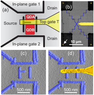
An outline of our structure is shown in Fig. 1(a). Two LAO based quantum dots are connected via 80–90 nm wide point contacts to the source and drain reservoirs. In-plane gates 1 and 2 allow to tune the electrochemical potential of the adjacent dot and tunneling barriers. The dots are connected by a 100 nm wide opening to allow for tunnel coupling. The opening is covered by a top-gate electrode on the surface for electrostatic tuning of the interdot coupling. Due to the added depletion of the tunneling barrier underneath, the top-gate can be operated at voltages which are not fully depleting the common 2DES drain contact.
Our fabrication scheme starts with a GaAs/AlGaAs-heterostructure suitable for LAO. Our heterostructure contains a two-dimensional electron system (2DES) with a low temperature mobility of m2/Vs and a sheet density of m-2 located 34 nm underneath the surface. The layer sequence consists of (from top to bottom): a 5 nm thick GaAs cap layer, 8 nm of AlGaAs, the Si--doping, a 20 nm wide AlGaAs barrier, and 100 nm of GaAs. Using standard photolithography we fabricate a mesa and Au/Ge/Ni ohmic contacts. Three nano-lithographic steps which have to be carefully aligned relative to each other follow: (1) define a common coordinate system for the following steps by producing Cr/Au markers using e-beam lithography, (2) LAO of the basic double-dot with in-plane gates, and (3) add the metallic finger gate with e-beam lithography.
In the first step, we apply e-beam lithography to pattern a metal layer consisting of 7 nm Cr and 30 nm Au for markers. Metallic alignment markers are needed to define a common e-beam/LAO coordinate system because the oxide lines produced by LAO are not visible in the electron microscope when covered by PMMA e-beam resist. We use two sets of markers: One set of markers is placed close to the center of the structure and used to check the alignment of the later LAO step with the AFM. The other one is placed farther outside where it is safely scanned with the electron microscope to align the final e-beam step without exposing resist in the central dot region. In addition, we produce the coarse part of the gate which is used as an additional marker for LAO. This is shown in Fig. 1(b). The proximity of the LAO markers to the critical center of the structure allows to align the later LAO step with a high absolute accuracy without suffering from distortions of the AFM piezo and a limited relative AFM resolution at large scanning fields.
For the AFM lithography which is employed in the second nanolithography step, we use our LAO scheme described in Ref. Keyser et al. (2000). Local oxidation of the heterostructure surface locally modifies the band structure and depletes the 2DES underneath. This directly transfers the oxidized pattern from the surface into the electronic system. We fabricate the basic double dot structure shown in Fig. 1(b) and (c). All oxide lines are about 100 nm wide and create insulating barriers in the 2DES. To align the AFM lithography we use the coarse part of the gate produced in the previous e-beam step. After oxidation, we scan the LAO structure and the inner marker set with the AFM to check the alignment accuracy and to compensate for a possible error in the next step.
We complete our sample by adding the 100 nm wide gate finger (7 nm Cr/30 nm Au) using e-beam lithography. For alignment we use the outer marker set from step (1).
The result is shown in Fig. 1(d). The figure illustrates how crucial an exact alignment of e-beam and AFM lithography relative to each other is. Since the width of the channel between the in-plane gates is 800 nm, we need to control the vertical position of the finger gate with an accuracy which is better than 50 nm. Only an exactly positioned finger gate allows to influence mainly the interdot coupling instead of the tunneling barriers to the reservoirs. This accuracy is achieved with the scheme described above.
The tunable double quantum dots are investigated in transport measurements in a 3He/4He-dilution refrigerator at a base temperature of 50 mK. We use a standard lock-in technique to measure the differential conductance with an AC-excitation voltage of 10 V at a frequency of 16 Hz.
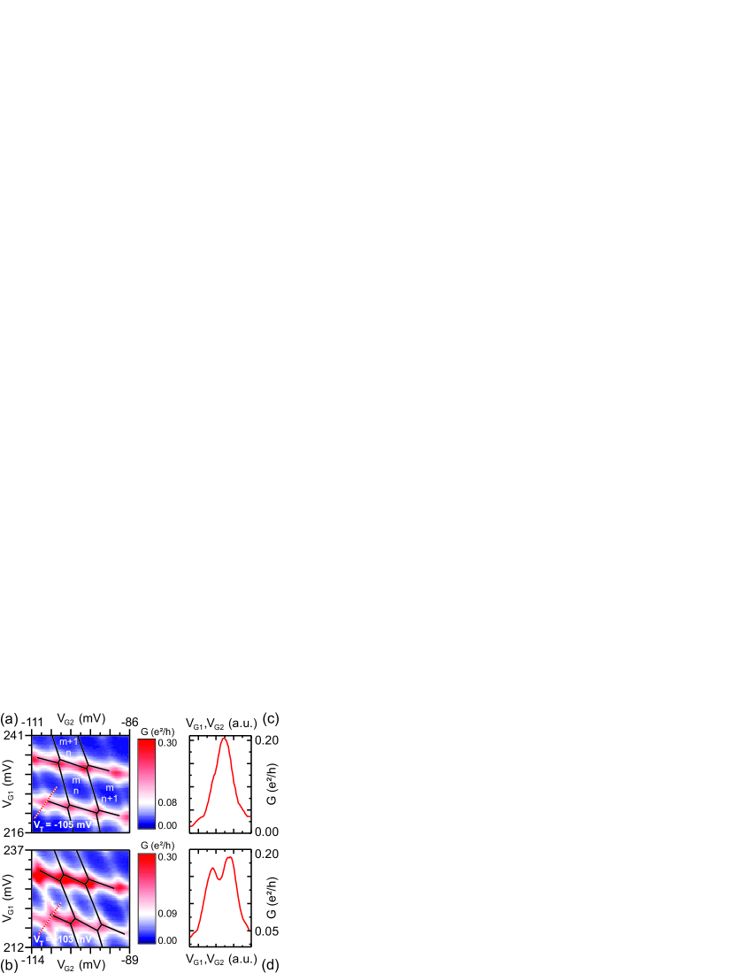
Figure 2(a) shows an image of the differential conductance as a function of in-plane gate voltages and . Both dots are weakly coupled to the reservoirs. In the low-conductance regions the electron number on dot is and on dot is . is stable. The nearly horizontal lines denote changes of the charge on dot by one electron, i. e. transitions from to . The nearly vertical lines denote the respective transitions for dot . At the intersections of both types of lines, both dots are in resonance with each other. This situation corresponds to transitions from to . In Figure 2(a), each of these intersections is just split into two triple points indicating a weak interdot coupling van der Wiel et al. (2003). We have increased the top gate voltage from mV to mV in Figure 2(b). The splitting of the triple points has clearly increased leading to more obvious hexagonal Coulomb blockade domains. This indicates a stronger interdot coupling achieved by tuning the top gate voltage . The traces in Figures 2(c) and 2(d) illustrate the increase of the splitting of the triple points with increasing top gate voltage (dashed lines in Figs. 2(a) and 2(b)).
The quantum dots are totally isolated from each other when we apply a top-gate voltage mV. We then get the signature of two non-interacting parallel quantum dots. To completely deplete the two-dimensional electron gas in absence of an oxidized barrier a voltage of mV is needed. So, there still is a common drain contact when the dots are isolated at mV. At more positive top gate voltages, the interdot coupling increases. At , both dots have merged and we observe one single large quantum dot. Thus, at intermediate voltages the coupling of the two quantum dots is not purely capacitively but at some point tunnel coupling sets on.
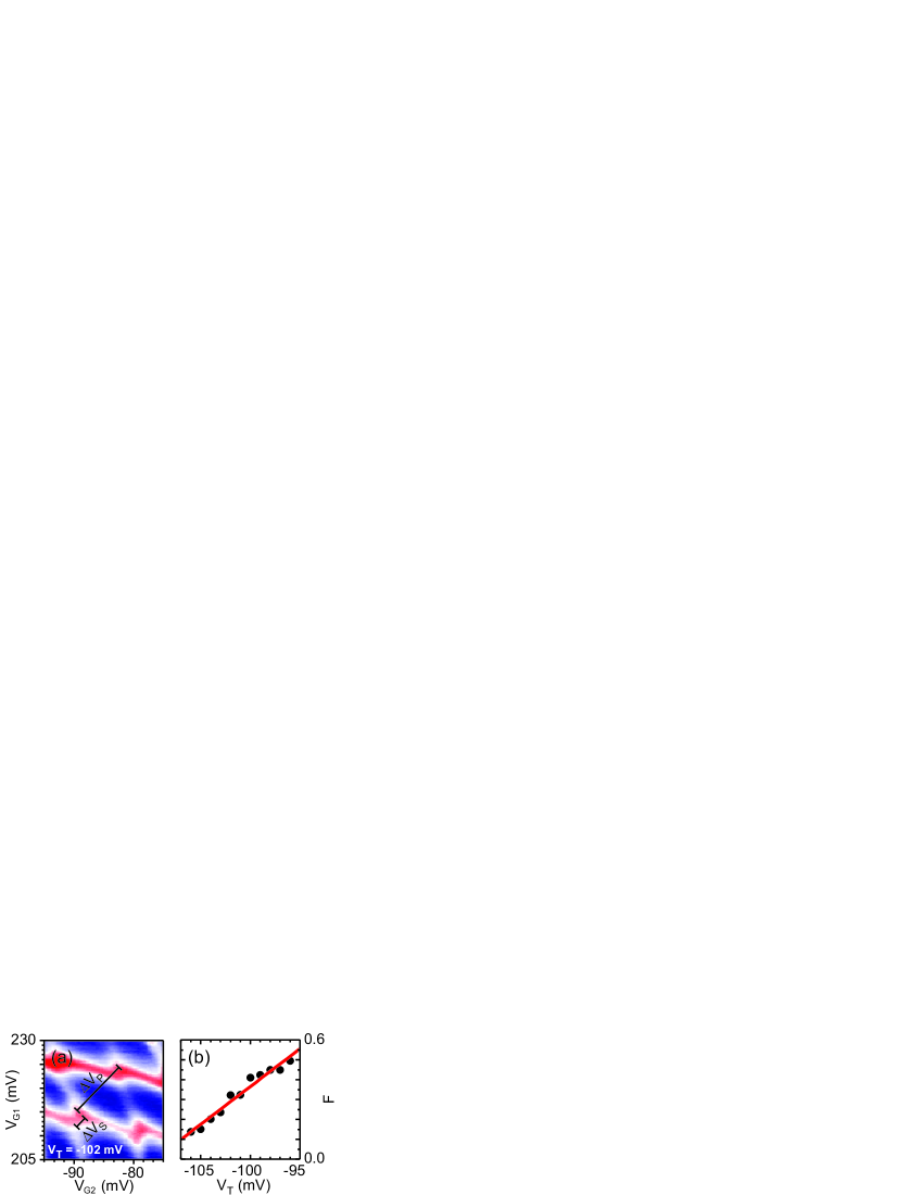
The dependence of the interdot coupling on top gate voltage is further investigated in Figure 3. The coupling is characterized by the fractional peak splitting with the Coulomb peak splitting and the period Golden and Halperin (1996). For totally decoupled dots is and for completely merged dots . We observe a linear dependence of on ranging from at mV to at mV in Figure 3(b). This large range of fractional peak splitting observed nicely demonstrates the tunability of the interdot coupling in our double-dot system.
In conclusion, we have demonstrated the combination of local anodic oxidation with an AFM and electron-beam lithography on a GaAs/AlGaAs heterostructure. We have shown that this combination of well-known fabrication schemes allows an easy fabrication of advantageous gate layouts. We have fabricated two parallel quantum dots with tunable interdot coupling. The electronic properties of this device were investigated in transport measurements. We have demonstrated the tunability of the interdot coupling.
We thank F. Hohls and U. Zeitler for helpful discussions and help with the measurement setup. This work has been supported by BMBF.
References
- Kouwenhoven et al. (1997) L. P. Kouwenhoven, C. M. Marcus, P. L. McEuen, S. Tarucha, R. M. Westerveld, and N. S. Wingreen, in Mesoscopic Electron Transport, edited by L. L. Sohn, L. P. Kouwenhoven, and G. Schön (Kluwer, Dordrecht, 1997), vol. 345 of Series E, pp. 105–214.
- Kastner (1992) M. A. Kastner, Rev. Mod. Phys. 64, 849 (1992).
- van der Wiel et al. (2003) W. G. van der Wiel, S. D. Franceschi, J. M. Elzerman, T. Fujisawa, S. Tarucha, and L. P. Kouwenhoven, Rev. Mod. Phys. 75, 1 (2003).
- Kouwenhoven et al. (2001) L. P. Kouwenhoven, D. G. Austing, and S. Tarucha, Rep. Prog. Phys. 64, 701 (2001).
- Blick et al. (1998) R. H. Blick, D. Pfannkuche, R. J. Haug, K. v. Klitzing, and K. Eberl, Phys. Rev. Lett. 80, 4032 (1998).
- Holleitner et al. (2002) A. W. Holleitner, R. H. Blick, A. K. Hüttel, K. Eberl, and J. P. Kotthaus, Science 297, 70 (2002).
- Loss and DiVincenzo (1998) D. Loss and D. P. DiVincenzo, Phys. Rev. A 57, 120 (1998).
- Hu and Sarma (2000) X. Hu and S. D. Sarma, Phys. Rev. A 61, 062301 (2000).
- Golovach and Loss (2002) V. N. Golovach and D. Loss, Semicon. Sci. Technol. 17, 355 (2002).
- Vandersypen et al. (2002) L. M. K. Vandersypen, R. Hanson, L. H. W. van Beveren, J. M. Elzerman, J. S. Greidanus, S. D. Franceschi, and L. P. Kouwenhoven, in Quantum Computing and Quantum Bits in Mesoscopic Systems (Kluwer, Dordrecht, 2002).
- Hofmann et al. (1995) F. Hofmann, T. Heinzel, D. A. Wharam, J. P. Kotthaus, G. Böhm, W. Klein, G. Tränkle, and G. Weimann, Phys. Rev. B 51, 13872 (1995).
- Molenkamp et al. (1995) L. W. Molenkamp, K. Flensberg, and M. Kemerink, Phys. Rev. Lett. 75, 4282 (1995).
- Adourian et al. (1999) A. S. Adourian, C. Livermore, and R. M. Westervelt, Appl. Phys. Lett. 75, 424 (1999).
- Holleitner et al. (2001) A. W. Holleitner, C. R. Decker, H. Qin, K. Eberl, and R. H. Blick, Phys. Rev. Lett. 87, 256802 (2001).
- Fujita et al. (1996) J. Fujita, Y. Ohnishi, Y. Ochiai, and S. Matsui, Appl. Phys. Lett. 68, 1297 (1996).
- Ishii and Matsumoto (1995) M. Ishii and K. Matsumoto, Jpn. J. Appl. Phys. 34, 1329 (1995).
- Held et al. (1998) R. Held, T. Vancura, T. Heinzel, K. Ensslin, M. Molland, and W. Wegscheider, Appl. Phys. Lett. 73, 262 (1998).
- Keyser et al. (2000) U. F. Keyser, H. W. Schumacher, U. Zeitler, R. J. Haug, and K. Eberl, Appl. Phys. Lett. 76, 457 (2000).
- Fuhrer et al. (2001) A. Fuhrer, S. Lüscher, T. Ihn, T. Heinzel, K. Ensslin, W. Wegscheider, and M. Bichler, Phys. Rev. B 63, 125309 (2001).
- Golden and Halperin (1996) J. M. Golden and B. I. Halperin, Phys. Rev. B 54, 16757 (1996).