Tailoring the photonic bandgap of porous silicon dielectric mirror
Abstract
A systematic method to fabricate porous silicon one dimensional photonic crystals has been engineered to have a photonic bandwidth up to 2000nm. The observation of the tailorability of the photonic bandgap (PBG) underscores the requirement of the large refractive index contrast for making broad PBG structures. In this letter, we present the fabrication and characteristics of such structures that may be promising structures for a large variety of applications.
Dielectric mirrors can reflect light for any direction of propagation in specific wavelength regionsjohn - john1 . This property will allow the creation of all-optical integrated circuits as it can be used to confine, manipulate and guide the photons. The advantage of a dielectric mirror over metallic ones is due to the dispersive and absorbing regions in the visible and infrared spectra of metals handbook . This kind of dielectric photonic band gap (PBG) structures have already been used in vertical-cavity surface-emitting lasers breiland , dielectric interference filters Hetch , sensors sensor and other devices.
Alternating layers of material with different dielectric constant are the simplest possible photonic crystals known so far. These dielectric multilayer films act as a perfect mirror for light with a frequency within a sharply-defined gap. For a fixed number of periods, this PBG increases, as the ratio of the refractive indices of the two layers (, high, H, and low, L, refractive index ) increases john ,Pavesi , and for a fixed ratio of refractive indices, upto a certain limit, the PBG increases with the number of periods Pavesi . In this letter we propose an idea to tailor the PBG structures, ranging from few nanometers to 2000 nm or more, for two different values of refractive indices, () without the prerequisite of a huge contrast. The idea has been successfully implemented experimentally on porous silicon.
Porous Silicon (pSi) is already considered as a promising material for photonic applications selena . This material can be fabricated with electrochemical etching of silicon with HF. In this material, the porosity is a linear function of the current density for a specific HF concentration and anodization time Pavesi and is known to show a refractive index contrast for different porosites theiss . Therefore, a periodic pulse alternating between two different current densities has been a convinient procedure to fabricate multilayer pSi films Pavesi ,selena , Canham . The change of the current density does not affect the previously formed pSi layer because silicon dissolution occurs at the silicon electrolyte interface Theib .
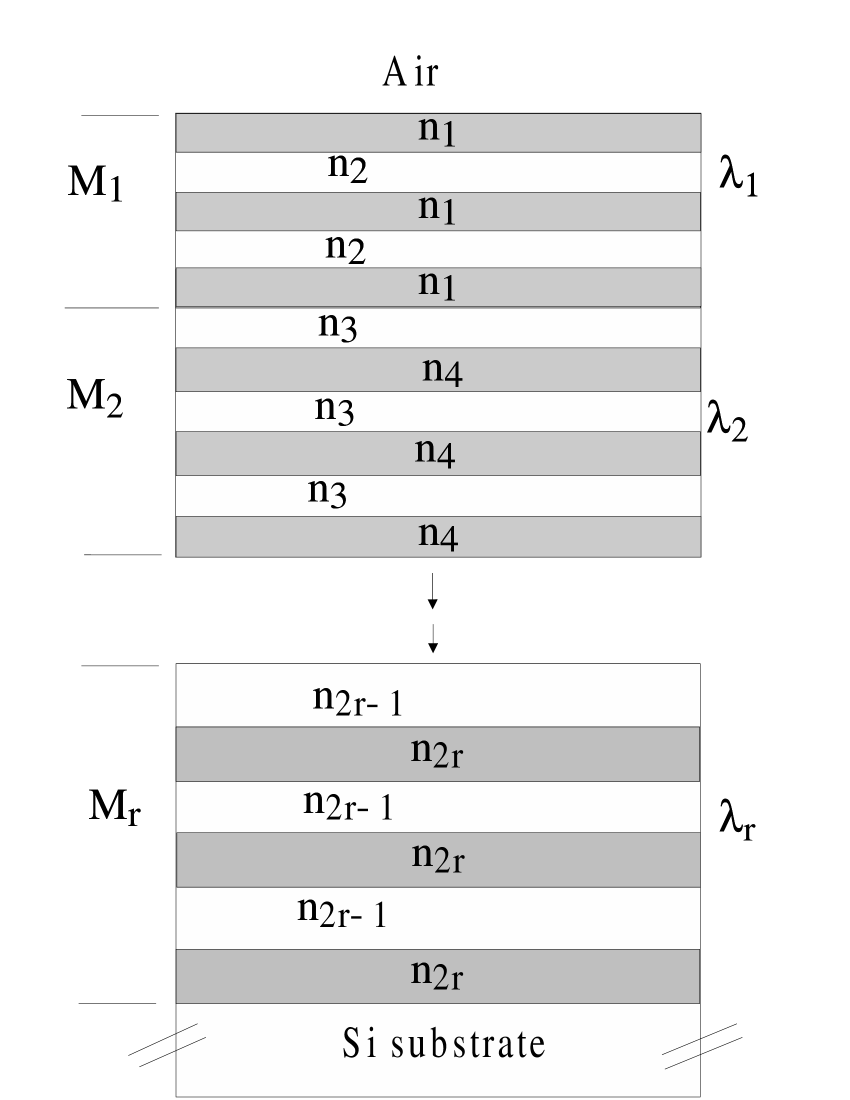
The multilayer pSi one dimensional-PBG structures known till now had the PBG of less than 500nm Pavesi selena . What we require is an easy method to modify the PBG of the structure according to our requirements. For the first time, through this letter, a technique to tailor the PBG structures, is successfully materialized on pSi multilayer mirrors. Stacks of (, with being the real thickness) mirrors have been prepared for different wavelengths in the visible and near infrared region (one submirror after the other submirror). The number of submirrors fabricated in a single structure varies from 2 to 80. Each mirror is designed for a different wavelength and can consist of 2.5 to 20 periods according to the requirements and the region we want to work with. Thus, the number of pSi layers can go up to 700. The exact selection of the -values depends on the application which will be discussed in the latter part of the paper.
Our method has been inspired by the ladder structure simulated by Kavokin et al. kavokin in order to observe photonic Bloch oscilations. The structures proposed are coupled microcavities, but here we present the structures without cavities, considering only dielectric Bragg mirrors (DBM). Of course, ladder structures can be prepared by different techniques, i.e., Molecular Beam Epitaxy, Metal Oxide chemical Vapor Deposition, etc. However in this letter, we use a cheap, easy and fast techinque to produce the same.
We have fabricated pSi multilayers by wet electrochemical etching viv of highly boron doped substrate (p+, 0.001-0.005 ). In order to have better interfaces, an aqueous HF/ethanol/glycerol electrolyte with 15% HF, 75% ethanol and 10% glycerol servidori concentration is used to anodize the silicon substrate. In addition, in order to maintain a constant HF concentration over the interface between Si and pSi under chemical attack, during the etching process a peristatical pump is used to circulate the electrolyte within the Teflon cell. Anodization begins when a constant current is applied between the silicon wafer and the electrolyte by means of an electronic circuit controlling the anodization process. To stabilize the pSi multilayer structure, all the samples are thermally oxidized in an oxygen ambient at 900 0C for 10 min fauchet . Oxidation induces a blue shift in the peak reflectivity due to the decrease in the refractive indices of the layers. In our structures, the multilayers have alternating porosities of the order of and . The time taken in the etching process varies from few minutes to 3 hours. Hence to make the surface stable, the first layer is always a low porosity layer and made 10-20 nm thicker than usual for thick structures (more than 20 microns). The refractive indices of the pSi layers have been estimated using reflectivity spectra of 2 m thick single layers at 1500nm. Scanning electron Microscopy (SEM) was used to examine the structural features of the films. The reflectivity spectra of the samples are taken with a Shimadzu UV3010 ultraviolet-visible-near infrared spectrophotometer at 5 degree incidence.
The schematic of the structures can be seen in Fig.1. The idea is to make one submirror after another submirror like a continuum array of submirrors. The specific range of -values depends directly on the application. For instance, a mirror reflecting the complete near infrared (NIR) range (800 to 2500 nm) only; for this we need to select the different wavelengths in this specific range in a way that the PBGs of respective submirrors overlap and give us a continuous PBG reflecting the full NIR range. For designing the mirrors for the latter part of the visible region and the NIR region, we have empirically selected the values as follows. First select the starting -value and then the subsequent -values obey a simple relation , where represents the submirror number. This selection has been performed and shown in the latter part of the letter.
We have made various structures composed of single mirror with 10 periods (one period consists of one low porosity and one high porosity layer) up to a mirror composed of a set of 80 submirrors. The total number of layers varies from 20 to 650 respectively. Taking into account that in the wide PBG structures the anodization time is of the order of hours, to make the structure more stable the first mirror always starts with a high refractive index layer, consisting of 2.5 to 4.5 periods. The subsequent submirrors consists of 3 to 5 periods reducing the etching time without affecting the flatness of the photonic band gap.
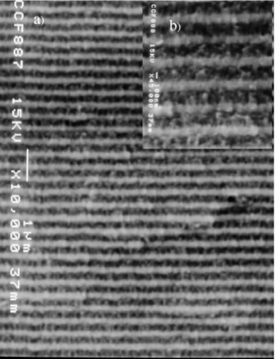
Fig. 2(a) shows cross sectional SEM images of 9 out of the 54 submirrors in the complete structure designed for the partial visible and complete near infrared region. This image shows a continuum array of submirrors prepared using , designed by taking with a refractive index contrast given by . The reflectance spectrum of this structure is shown in Fig.3(b).
The absolute reflectance spectra of some of the structures have been shown in Fig. 3. The absolute reflectivity of commercially available Aluminium (Al) mirrors with a SiO overcoat (as bare silicon is prone to oxidation and loses its reflectivity) is shown in Fig. 3(a) oriel . The figure clearly shows an absorption in the visible region. From 400nm to 2500 nm the reflectivity varies between 85-90% with a dip to 75% at around 825nm. Taking this mirror as a reference (available with the Shimadzu UV3101 UV-vis-NIR spectrophotometer) the reflectivity spectra of our structures have been measured. Hence in the visible region, the reflectance shown by most of our structures was higher than that for the Al mirror. Thus, the data have been corrected for the Al mirror response. Fig.3(b)-(d) show the absolute reflectance of few examples demonstrating the successful implementation of the idea. In fig 3(b) we present the response of the mirror shown in Fig.2. It has the PBG for the partial visible and complete NIR region i.e. from 615nm to 2450nm. The absolute reflectance can be clearly seen within 85-100% which is clearly 2-20 % more than that for the Al mirror from 615-1200nm. In fig 3(c) we plot the absolute reflectance of a mirror designed for the complete visible range. The absolute reflectance of this mirror is higher than the Al mirror from 390 to 650 nm range, as can be seen, from the inset which shows the raw data coming from Shimadzu UV3101 UV-vis-NIR spectrophotometer having Al mirror as reference. This mirror is composed by 77 submirrors, with the starting wavelength 450nm and the subsequent DBMs are determined by the relation having 4 periods in each submirror. The refractive index contrast used was .
The reflectivity of a mirror reflecting two different wavelength ranges has been shown in Fig. 3(d). This particular mirror is composed by two submirrors, one prepared for 600 nm () and another for 1700 nm () with 10 periods each. The idea is to show how we can change the refractive index contrast from one submirror to another submirror if required. Theoretical simulations have been done for all the tailored PBG structures and seen to be in agreement with the experimental reflectivity spectra va
Here we can clearly see the enhancement of the PBG width with the increase in the number of submirrors. We can very well understand that this broad PBG is due to the overlapping of all the PBGs of the submirrors designed for different wavelengths. The advantage of these mirrors over metallic mirrors (Al or silver) is their selective nature and higher reflectivity. For example, designing a mirror for the complete NIR range without significant reflection from the visible range or viceversa will be excellent for different applications.
It is important to stress that Pavesi group too has developed photonic structures with wide photonic band gap using aperiodic porous silicon layers oton .
Apart from the structures shown in Fig. 3 we have tailored the PBG for many other mirrors, for example in the spectral ranges of 356-650nm, 400-600nm, 600-1200nm, 600-2000nm, etc. The idea is to design a PBG of desired width and at required wavelengths. Here we present just few examples with a lot of scope for improvement. It will also stimulate the interest of making better filters based on single microcavity microcavities , because with the method presented here we are able to increase the high reflecting range on both sides of the cavity.
For the first time, it has been made possible to tailor the PBG of the dielectric mirrors, for the partial UV and complete vis-NIR range (from 356nm to 2500nm) to have desired width at required wavelenths. These mirrors are easy to prepare, selective and more reflective than the commercially available Al mirrors.
We gratefully acknowledge the useful discussions with Dr. Miguel Robles and help provided by Jose Campos, Dr. Oswaldo Flores (CCF-UNAM).
References
- (1) Photonic Crystals: Molding the flow of light, By John D. Joannopoulos, Robert D. Meade, Joshua N. Winn Princeton University Press (1995) pg. 41.
- (2) Y. A. Vlasov, X-Z. Bo, J.C. Sturm and D. J. Norris, Nature, 414 (2001)289
- (3) E.Yablonovitch, Phys. Rev. Lett.58 ,2059(1987)
- (4) J.D. Joannopoulos, P.R.Villeneuve,and S.Fan Nature 386, 143(1997)
- (5) Americal Institute of Physics Handbook, Coordinating editor Dwight E. Gray,(1972) pg 6- 124
- (6) W.G. Breiland, A.A. Allerman, J.F. Klem and K.E. Waldrip. MRS Bulletin, (2002) 520
- (7) E.Hetch Optics, Addison-Wesley pg. 377(1987)
- (8) W. A. Challener. US patent Application No.20020018610
- (9) L.Pavesi, La Revista del Nuevo Cimento 20, 18 (1997)
- (10) S. Chan and P.M.Fauchet, Appl. Phys. Lett. 75, 274(1999); J.E. Lugo, H.A. López, S. Chan and P.M. Fauchet, J. Appl. Phys. 91, 4966 (2002).
- (11) W. Theiss and S. Hilbrich, Properties of porous silicon, edited by L.T.Canham EMIS Datareviews series pg. 223
- (12) L.T.Canham, M.P.Stewart, J.M.Buriak et al. Phys. Stat. Sol. A 182 521(2000)
- (13) W. Thei Surf. Sci. Rep. 29, 91 (1997)
- (14) A. Kavokin, G.Malpuech, A.Di Carlo P. Luigi and F. Rossi Phys. Rev. B 61, 4413 (2000). G.Malpuech, A. Kavokin, G. Panzarini, and A.Di Carlo, Phys. Rev. 63, 035108 (2001).
- (15) V. Agarwal, R.M.Mehra, P.C.Mathur. Thin Solid Films 358 (2000)196.
- (16) M.Servidori, C. Ferrero, S.Lequien et.al.Sol. State Commun.118 (2001) 85.
- (17) S.P.Duttagupta, P.M. Fauchet , Mat. Res. Soc. Sym. Proc. 358, 381 (2000). Fauchet P.M., Tsybeskov, L. Hirschmann, K.D. US Patent 6,017,773.
- (18) The book of photon tools by Oriel Instruments. pg 14-8.
- (19) V. Agarwal and J.A.del Río (unpublished)
- (20) Y.Zhou, P.A.Snow, P.S.J.Russell Mater.Sci.& Eng. B 81, 40 (2001); L.Pavesi, V. Mulloni, J.Lumin. 80, 43 (1999).
- (21) C.J. Oton, L. Dal Negro, P. Bettotti, L. Pancheri, Z. Gaburro and L. Pavesi ”Photon states in one dimensional photonic crystals based on porous-silicon” in ”Radiation-matter interaction in confined systems” Ed. by L.C. Andreani, G. Benedek, E. Molinary, Societa Italina di Fisica, Bologna pp. 303, (2002).