In-plane Magnetic Field Dependent Magnetoresistance
of Gated Asymmetric Double Quantum Wells
Abstract
We have investigated experimentally the magnetoresistance of strongly asymmetric double-wells. The structures were prepared by inserting a thin Al0.3Ga0.7As barrier into the GaAs buffer layer of a standard modulation-doped GaAs/Al0.3Ga0.7As heterostructure. The resulting double-well system consists of a nearly rectangular well and of a triangular well coupled by tunneling through the thin barrier. With a proper choice of the barrier parameters one can control the occupancy of the two wells and of the two lowest (bonding and antibonding) subbands. The electron properties can be further influenced by applying front- or back-gate voltage.
keywords:
Double-layer two-dimensional electron system, Magnetotransport, Gate voltagePACS:
74.40.Xy , 71.63.Hk, , , , , and
1 Introduction
A magnetic field applied parallel to the quasi-two-dimensional systems of electrons confined in double-well structures is known to couple strongly to the electron orbital motion and to change dramatically the electron energy spectra. The magnetoresistance oscillation observed on coupled double quantum wells represents a striking manifestation of van Hove singularities in the -dependent density of states, corresponding to the depopulation of the antibonding subband at a critical field , and to the splitting of the Fermi sea into two separated electron sheets at a second critical field [1, 2, 3, 4]. There can also be the third critical field [5] at which the system returns to the single layer state due to depletion of the triangular well.
2 Experiments
Strongly asymmetric double-well structures were prepared (by MBE method) by inserting a thin Al0.3Ga0.7As barrier into the GaAs buffer layer of standard modulation-doped GaAs/Al0.3Ga0.7As heterostructures. The resulting double-well system consists of a nearly rectangular well and of a triangular well. The bonding and antibonding subbands are formed by tunnel-coupling of the ground states in individual wells.
The resulting separation of the bonding and antibonding levels depends on the position and on the thickness of the barrier. The minimum separation is achieved if the barrier is located close to the center of mass of the two-dimensional electron layer. With the barrier closer to or farer from the interface the bonding and antibonding subbands become more separated.
Two types of structures with similar bonding and antibonding energy levels can be prepared: (i) The barrier is far from the interface and only a small part of electrons is in the triangular well. (ii) The barrier is close to the interface and the majority of electrons is in the triangular well.
The occupancy of the wells can be further modified by applying front- or back-gate voltage. The back-gate voltage will influence strongly the structures of the first type while the samples of the second type will be more sensitive to the front-gate voltage.
The response of a structure to the applied in-plane magnetic field depends on its type.
For both types the Fermi contours are two concentric circles at . The in-plane field induces a transfer of antibonding electrons to the bonding subband and the shift of the centre of mass of the electron layer closer to the interface [4].
The Fermi contour of the antibonding subband changes its shape, shrinks and, at a critical field , disappears. All electrons occupy only the bonding subband and form a wide single layer. The magnetoresistance approaches a pronounced minimum as the density of states (DOS) is halved and, therefore, also the electron scattering rate.
Upon further increasing , the system undergoes a transition from a single-layer to a bilayer state. A neck in the peanut-like Fermi contour becomes narrower and, at , the contour splits into the Fermi lines of two independent electron sheets localized in the rectangular and triangular wells. At this second critical field, the DOS has a logarithmic singularity and the magnetoresistance reaches a sharp maximum.
Above , the shift of the electron sheet towards the interface continues. In the first type of structures all electrons are transfered into the rectangular well at a third critical field and the 2D system re-enters the single-layer state [4]. An example of the magnetoresistance trace and the calculated DOS is in Fig. 1.
The aim of this paper is to study the influence of front- and back-gate voltages on the above mentioned critical fields.

Two samples grown by MBE were studied. The Sample A with a wide rectangular well and the Sample B with a narrow rectangular well. In Table 1, the width of the rectangular well is denoted by , the width of the barrier is . The experiments were carried out at temperature K, using low-frequency (13 Hz) technique.
| Sample | |||||||
|---|---|---|---|---|---|---|---|
| (nm) | (nm) | ||||||
| A | 10 | 3.4 | 3.02 | 0.25 | 3.27 | 1.16 | |
| B | 7 | 1.7 | 2.64 | 0.57 | 3.21 | 0.97 |
The presented characteristics of 2DEG have been extracted from the data taken in perpendicular magnetic fields. The total electron concentration and the electron mobility were calculated from the low-field Hall and zero-field resistivities, respectively. The partial concentrations of electrons in the subbands, and , were determined from the period of Shubnikov-de Haas (SdH) oscillations.
3 Results and discussion
3.1 Sample A
The Sample A has a 10 nm wide rectangular well and only the minority of electrons is behind the barrier in the triangular well. Therefore, it is a good candidate for application of the back-gate voltage. (The magnetoresistance obtained for zero gate voltage is shown in Fig. 1.)
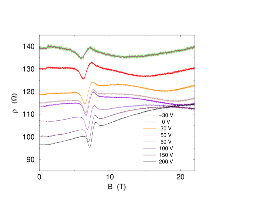
Experimental curves for a range of back-gate voltages are presented in Fig. 2. The back gate has strong effect on the electrons of low-populated triangular well. While the critical fields and do not depend substantially on the applied gate voltage, the third critical field (at which the system returns to the single layer state) is very sensitive to the change of the total concentration induced by the back-gate voltage. An increase of due to positive back-gate voltages leads to a shift of to higher magnetic fields. At higher possitive back-gate voltages there are too many electrons in the triangular well and the minimum in magnetoresistance corresponding to is beyond the available magnetic fields.
3.2 Sample B
The Sample B has a 7 nm wide rectangular well. The application of the front-gate voltage has even more dramatic effect on its electronic structure than the back-gate on the Sample A.


As it can be deduced from resistivity curves in Fig. 3, the negative gate voltage reduces the electron concentration and is able to empty the antibonding subband without application of the in-plane magnetic field. At the same time, the sheet of electrons is repulsed from the interface behind the barrier, i.e into the triangular well.
Qualitatively, the variation of the resistivity is expected to be proportional to the scattering rate (which is approximately doubled at the crossover from the single-subband to the double-subband occupancy) and inversely proportional to the concentration . This is schematically sketched in Fig. 3 by dotted lines. The zero-field resistance exhibits an oscillation corresponding to this scheme with the crossover around V. The single-subband to the double-subband occupancy is confirmed by a sudden change of period of SdH oscillations observed on the magnetoresistanence trace measured at T. The fast oscillations for V are attributed to the single-subband occupancy, the slow oscillation above V are due to electrons in the bonding subband.
The quantitative results for the dependence of partial concentrations and of the mobility on , obtained from low field magnetoresistance measurements, are summarized in Fig. 4. Here we assume that the Hall voltage determines the total concentration, , and only electrons in the bonding subband are responsible for the SdH oscillations, , when two subbands are occupied.

Magnetoresistance traces for Sample B, measured in parallel field configuration for different front-gate voltages, are displayed in Fig. 5. Positive gate voltages shift the critical fields and to higher values as (and mainly ) increase. As the negative reduces , shifts to lower fields and the corresponding singularity becomes less pronounced. The same is true also for . While disappears as , we attribute the suppression of the logarithmic singularity at , related to the single-layer/double-layer transition, to the fact that, at most negative , no neck is formed on the Fermi contour, the Fermi contour does not split into two parts and no independent electron sheet is formed in the rectangular well.
4 Conclusions
The magnetic field oriented in parallel to the 2D electron system induces a deformation of the Fermi contours corresponding to bonding and antibonding subbands, depopulation of the higher occupied subband at the critical field , and the transition into the decoupled bilayer at the critical field .
With the small concentration of electrons in the triangular well, we can observe the third critical field at which the triangular well is emptied and the system returns to the single layer state. The critical field is strongly dependent on the back-gate voltage.
The negative front-gate voltage can empty the antibonding subband and suppress and in samples with small concentration of electrons in the rectangular well. In that case, no single-layer/double-layer transition occurs.
Acknowledgements
This work has been supported by the Grant Agency of the Czech Republic under Grant No. 202/01/0754, by the French-Czech project Barrande 99011, and by the European Community project “Access to Research Infrastructure action of the Improving Human Potential Programme”.
References
- [1] J. A. Simmons, S. K. Lyo, N. E. Harff, and J. F. Klem, Phys. Rev. Lett. 73, 2256 (1994); S. K. Lyo, Phys. Rev. B 50, 4965 (1994).
- [2] A. Kurobe, I. M. Castleton, E. H. Linfield. M. P. Grimshaw, K. M. Brown, D. A. Ritchie, M. Pepper, and G. A. C. Jones, Phys. Rev. B, 50, 4899 (1994).
- [3] T. Jungwirth, T. S. Lay, L. Smrčka, and M. Shayegan, Phys. Rev. B, 56, 1029 (1997).
- [4] O. N. Makarovskii, L. Smrčka, P. Vašek, T. Jungwirth, M. Cukr, and L. Jansen, Phys. Rev. B, 62, 10 908 (2000).
- [5] P. Svoboda, Yu. Krupko, L. Smrčka, M. Cukr, T. Jungwirth, and L. Jansen, Physica E, 12, 315 (2002).