Immittance Matching for Multi-dimensional Open-system Photonic Crystals
Abstract
An electromagnetic (EM) Bloch wave propagating in a photonic crystal (PC) is characterized by the immittance (impedance and admittance) of the wave. The immittance is used to investigate transmission and reflection at a surface or an interface of the PC. In particular, the general properties of immittance are useful for clarifying the wave propagation characteristics. We give a general proof that the immittance of EM Bloch waves on a plane in infinite one- and two-dimensional (2D) PCs is real when the plane is a reflection plane of the PC and the Bloch wavevector is perpendicular to the plane. We also show that the pure-real feature of immittance on a reflection plane for an infinite three-dimensional PC is good approximation based on the numerical calculations. The analytical proof indicates that the method used for immittance matching is extremely simplified since only the real part of the immittance function is needed for analysis without numerical verification. As an application of the proof, we describe a method based on immittance matching for qualitatively evaluating the reflection at the surface of a semi-infinite 2D PC, at the interface between a semi-infinite slab waveguide (WG) and a semi-infinite 2D PC line-defect WG, and at the interface between a semi-infinite channel WG and a semi-infinite 2D PC slab line-defect WG.
pacs:
42.70.Qs, 42.79.GnI Introduction
Photonic crystals (PCs) are artificial materials whose dielectric functions periodically vary.Yab ; John ; Ohtaka ; Kosaka ; Jo ; Sakoda The primary characteristics of PCs are photonic band gaps and peculiar dispersion relations, both of which enable the propagation of electromagnetic (EM) waves in PCs to be controlled. Recent interest in PCs has focused on “open-system PCs,”Jo ; Sakoda ; Noda ; Mekis ; Johnson ; Stefanou ; Yannopapas which are connected to other structures at their boundaries. Typically investigated are a finite PC contacting another medium and finite PC line-defect waveguides (WGs). In open-system PCs, the energy of propagating EM waves is transferred into or out of the PCs through the boundaries. This is in contrast to closed-system PCs, which are infinite in size and therefore contain all the energy at any time.
An open-system PC can be divided into a set of subsystems — the PC and the attached structures. Therefore, it should greatly facilitate designing open-system PCs if each subsystem is independently designed and then all the subsystems are assembled. Such a method has become well established for electrical circuit design. The behaviors of the electrical energy flows are predicted based on electrical immittance (impedance and admittance).Heaviside_Woods Two electrical circuits can be assembled without energy reflection at their interface if the electrical immittances of both circuits match. A complete electrical circuit system can thus be designed after designing each subsystem independently.
EM wave media including open-system PCs can be regarded as EM wave circuits, for which an analogous figure of merit, EM wave immittance, is similarly defined.Schelkunoff It is a ratio of the electric field to the magnetic field of a propagating or decaying wave in a single medium. In practice, it has been possible to design one-dimensional (1D) open-system PCs by using the EM wave immittance. Particularly notable is that the renormalized Fresnel coefficient for a semi-infinite 1D PC with an arbitrary unit cell has been defined using the EM wave immittance for Bloch waves.Ushida_1d_arc However, there is still difficulty in designing multi-dimensional open-system PCs. This is because the number of EM wave immittances that should be considered at a point on an arbitrarily shaped boundary increases with the number of structural dimensions. Specifically, the immittance of an EM wave with a given polarization is expressed as one parameter for a 1D PC, two parameters for a two-dimensional (2D) PC, and six parameters for a three-dimensional (3D) PC. Moreover, each parameter of an EM wave immittance is complex in general. Therefore, excessive computational cost would be needed to match every immittance parameter between two multi-dimensional subsystems.
One way to simplify the matching problem is to reduce the number of parameters by considering structural symmetry. Also, simplifying the parameters themselves is helpful, as has been suggested by Boscolo et al.Boscolo They pointed out that a propagating wave in a PC line-defect WG has a pure-real immittance on periodic symmetry planes normal to the direction of propagation. Similar findings have been obtained through analytical calculation of the impedance of 1D PCsKawakami_2 ; Ushida_1d_arc and through numerical calculation for 2D PCs.Noda_2 In this article, we take another approach to simplifying the matching problems — qualitative optimization of individual subsystems.
This paper is organized as follows. In Sec. II, we first prove that pure-real immittance is a common property of EM Bloch waves in 1D and 2D PCs, hence it can be used for any 1D or 2D open-system PC. We also prove that the pure-real property of the immittance is true for 3D periodic structures, but under a limiting condition. Then, in Sec. III, we present three examples of designing multi-dimensional open-system PCs. This analysis can be made because the immittance defined by using eigenmodes on the boundary of two semi-infinite regions (a PC and its external structure) can be determined from the eigenmodes of an infinite PC and its external structure. In Sec. III.1, we present a method for qualitatively evaluating the reflection at the surface of a semi-infinite 2D PC; the approximate availability of the perfect antireflection coating (ARC) method developed for a semi-infinite 1D PCUshida_1d_arc to a semi-infinite 2D PC is emphasized. These semi-infinite 2D PCs can be used for analyzing various applications such as add/drop multiplexers, dispersion compensators, polarization filters, and image processors.Kosaka ; Ohtera ; Notomi In Sec. III.2, we investigate a 2D line-defect WG that efficiently transmits EM energy to a channel WG. The semi-infinite 2D PC line-defect WG is a promising platform for ultra-compact photonic circuits.Johnson ; Yamada In Sec. III.3, we investigate the interface between a semi-infinite channel WG and a semi-infinite 2D PC slab line-defect WG as a typical 3D problem.Miyai All the applications of the proof are presented using the concept of immittance matching. Section IV devotes for conclusion.
II General proof for Immittance of Electromagnetic Bloch Waves
We begin our description of the proof with a general expression of EM Bloch waves. Assuming time harmonic EM waves, the general expression for an EM Bloch wave; Sakoda
| (1) | |||||
| (2) |
where and stand for the band index and Bloch wavevector, and functions and have lattice periodicity. The immittance of a Bloch wave is closely related to the energy flow conveyed by the wave; it is therefore useful to define a complex Poynting vector:
| (3) |
where the real (imaginary) part of is the density of the time-averaged (reactive) power flow.Fano
Here, we consider the time reversal state of Eqs. (1) and (2), which is written as
| (4) | |||||
| (5) | |||||
| (6) |
due to the even (odd) parity of electric (magnetic) field under time reversal operation.Jackson Eqs. (4)-(6) can be reduced toSakoda
| (7) | |||||
| (8) | |||||
| (9) |
Eqs. (7)-(9) express the time reversal degeneracy of the spin 1 particle (photon). Eqs. (7)-(9) will be used later.
Next, we consider a Poynting vector described using EM Bloch waves under a reflection operation in infinite 2D PCs. Figure 1 illustrates typical infinite 2D PCs with reflection plane . When the propagation direction of a Bloch wave is perpendicular to this plane, the electric Bloch wave is transformed by reflection operation into
| (13) | |||||
| (17) |
where , , and stand for the reflection operator, the inversion operator, and the rotation about the axis. Note that the obvious factor is omitted in Eqs. (13) and (17). Note also that this reflection operation () is not the symmetry operation of the -group at , but of the point group in an infinite 2D PC. Similarly, magnetic Bloch wave is transformed into
| (21) |
In the derivation of Eqs. (17) and (21), we use Eqs. (8) and (9). The non-zero components of EM waves in the Cartesian coordinate system are for TM and for TE polarization.TMTE
Accordingly, the Poynting vector described using the EM Bloch wave under reflection operation can be written as
| (24) |
On reflection plane , equals . Therefore, using Eqs. (3) and (24), we obtain
| (25) | |||||
| (28) | |||||
| (31) |
where , and at .
Q. E. D.
Eq. (31) means that the immittance is real in infinite 1D and 2D PCs on a plane when the plane is a reflection plane and the Bloch wavevector is perpendicular to the plane. It also means that the reactive power flow is zero for the Bloch wave on the plane under consideration.
For the case of an infinite 3D PC, Eq. (25) can be written as
| (32) |
Therefore, an additional reflection plane is required for removing the imaginary part of the impedance. When there is reflection plane at , some components of the EM waves vanish on the plane. They are called TM- or TE-like based on the analogy to infinite 2D PCs. Johnson_slab In this case, the impedance is real on the intersection line of the and planes.

III Applications of pure-real property of immittance
As a typical application of the above proof, we present a method reducing a reflection loss at the surface of a semi-infinite 2D PC, a semi-infinite 2D PC line-defect WG, and a semi-infinite 2D PC slab line-defect WG based on the concept of the immittance matching. The method for the immittance matching is extremely simplified since only the real part of immittance function for an infinite PC is needed for the analysis. The reflection coefficient of a semi-infinite PC should be determined via Bloch wave expansion in the semi-infinite PC and the expansion should be described by all the eigen modes of an infinite PC (i.e., including decaying waves).Minami However, here we investigate only the impedance of propagation modes. This is another merit of our method, that is , it is not necessary to know all the eigenmodes in our method for immittance matching problem. The information on the impedance of propagation modes can be used for qualitatively investigating the reflection in various types of open system PCs.
III.1 Semi-infinite 2D PC
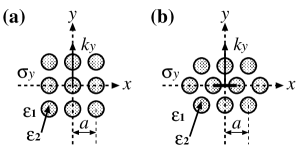
The geometry of the first example is shown in Fig. 1 (b). The parameters of the PC is summarized in the caption of Fig. 2.
Figure 2 (a) illustrates the dispersion relation of the TM polarization wave for the infinite 2D PC in the M direction.MPB Suppose that one considers the reflection at the surface of a semi-infinite PC made from the infinite PC cleaved at the plane shown in Fig. 2 (b). The incident wave is a normal incident plane wave propagating in vacuum. Then, one should calculate the immittance of the Bloch wave at by using the eigen mode of the infinite PC. The immittance of the Bloch wave is generally complex and has lattice periodicity of the infinite 2D PC. The impedance at calculated using propagating Bloch waves with is shown in Fig. 2 (b). The illustrated region is indicated by the thick solid line in Fig.1 (b). The impedance is normalized by the impedance in vacuum. Note that only the impedance of Bloch waves able to couple with an incident plane wave (“coupled modes”) indicated by “A” in Fig. 2(a) is plotted. Since the spatial modulation of bands B1 and B2 is flatter than that of bands B4 and B5 and the impedance is near the value in vacuum (i.e. impedance normalized by vacuum value is near one), the reflection loss of bands B1 and B2 at the frequency is lower than that of bands B4 and B5 for the normal incidence of a plane wave. In addition, the flatness of the impedance enables us to reduce the reflection loss by using an antireflection coating (ARC) method developed for semi-infinite 1D PCs.Ushida_1d_arc In this case, since the plane is a reflection plane, thickness and refractive index of the ARC can be estimated using
| (33) | |||||
| (34) |
where is the normalized thickness of the ARC, is a wavelength in vacuum, is the refractive index of a semi-infinite medium, and for TM polarization. Accordingly, the reflection loss is easily removed by using Eqs. (33) and (34). If a spatially flat impedance appears in the TE polarization case, Eq. (34) can be used by replacing with to reduce the reflection loss of the TE polarization waves.
III.2 Semi-infinite 2D Line-defect PC Waveguide
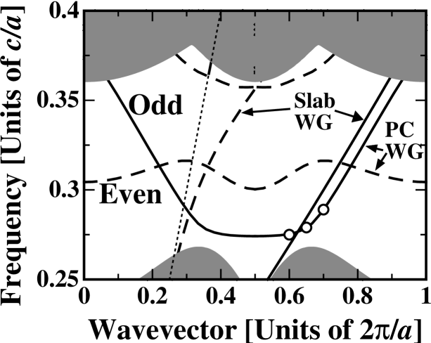
The second example is related to the interconnection between a semi-infinite slab waveguide (WG) and a semi-infinite 2D PC line-defect WG, or “PC WG.” The connection between different WGs is important to realize the ultra-minute photonic circuits. Although some numerical investigation were made for similar structures,Yamada ; Xu ; Adibi ; Adibi2 ; Mekis2 ; Mekis3 ; Miyai we investigate it based on the concept of immittance matching. The semi-infinite PC WG is made by removing a row of air holes in the K direction from a semi-infinite 2D triangular lattice of air holes with radius and in a medium with . The slab WG has width and permittivity (the same as the of the PC). The dispersion relation of the propagation modes of the infinite slab WG and infinite PC WG are shown in Fig. 3.MPB The polarization is TE; that is, the magnetic wave is parallel to the slab and to the axis of air holes in the infinite 2D PC.TMTE Since the both of the slab WG and the PC WG have reflection plane bisecting these WGs, the propagation mode has even (broken line) or odd (solid line) parity under reflection operation, as shown in Fig. 3. The shaded region indicates the projection band structure. When K, the dispersion relation of the infinite slab WG is similar to that of the infinite PC WG. Such situation was called -matching (wavevector matching) by Mekis et al.Mekis2 ; Mekis3 as a mechanism to reduce the reflection from the joint of a distributed Bragg reflector WG and a 2D PC WG with square lattice of rods. On the other hand, the exactly derived renormalized Fresnel coefficients of a semi-infinite 1D PC did not include Bloch wavevector explicitly.Ushida_1d_arc The analytical investigation of a relation between immittance matching and -matching will be published elsewhere.Tokushima
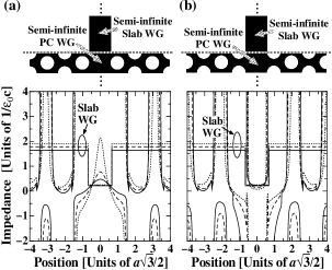
Here, we investigate the direct connection between a semi-infinite slab WG and a semi-infinite PC WG based on the immittance matching. Figure 4 illustrates the dependence of the spatial distribution of the impedance on the wavevector and on the surface of the semi-infinite PC WG. The difference between Figs. 4 (a) and (b) is the position of the surface [shown as a dotted line in the diagram above each graph in Figs. 4(a) and (b)] of the semi-infinite PC WG connected with the semi-infinite slab WG. For the semi-infinite slab WG, the impedance is homogeneous inside and outside the slab region, which shows a rectangular spatial distribution. In addition, the impedance at a surface is independent of the cleaved position of the infinite slab WG. For the semi-infinite PC WG, the impedance depends strongly on the position of the surface of the semi-infinite PC WG due to the spatial periodicity of the impedance in the infinite PC WG. Moreover, the impedance on a surface has a complex spatial distribution on the surface. Divergence appears where the magnetic wave vanishes. Divergence in a differential impedance appears at normalized position , for Fig. 4 (a), and at , for Fig. 4 (b). The divergence is due to the discontinuity of the electric wave perpendicular to the air holes at the surface of the semi-infinite PC WG. From the Poynting vector calculation, we can confirm that the EM energy of these propagation modes concentrates around the normalized position .Boscolo Therefore, region (the width of the slab WG) is quite important for analyzing the immittance matching between the semi-infinite slab WG and semi-infinite PC WG modes. In this region, the impedance matching between the semi-infinite slab WG and the semi-infinite PC WG modes of Fig. 4 (b) is better than that of Fig. 4 (a). Hence, the geometry of Fig. 4 (b) is better for reducing reflection loss. In addition, when the wavevector approaches the 1st Brillouin zone boundary, the difference in the impedance between the slab WG and the PC WG modes becomes noticeable. Therefore, in a direct interconnection between the semi-infinite slab WG and the semi-infinite PC WG, the reflection loss of modes with is higher than that with .
III.3 Application to 3D structures –Semi-infinite 2D PC Slab Line-defect WG–
In this section, we investigate the connection between a semi-infinite 2D PC slab line-defect WG and a semi-infinite channel WG based on the concept of immittance matching. Schematic illustrations of two kinds of connections are shown in Figs. 6 (a) and (b). The structures are sandwiched by two semi-infinite vacuum regions in the vertical direction (-axis direction), hence they are 3D in nature. The 2D PC slab consists of a triangular lattice of air holes. The line defect WG is introduced into the slab by filling the air holes in a row. The detailed parameters of these structures are given in the caption of Fig. 5. The width and thickness of the channel WG are and , where is the radius of the air holes and is the lattice constant.
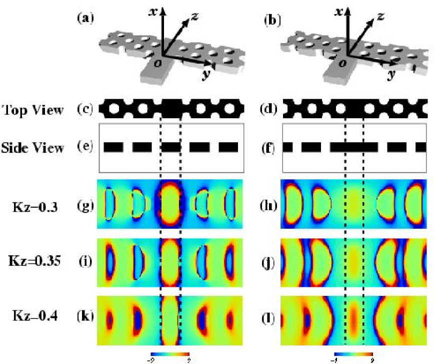
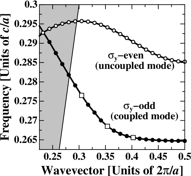
Figure 5 illustrates the energy dispersion relation of the TE-like modes of an infinitely long 2D PC line-defect WG. Fundamental EM mode propagating in the channel WG can be coupled only with the “odd” modes of 2D PC slab WG in the ideal case [Mode symmetry is defined by the symmetry operation associated with the symmetry plane ( at y=0) bisecting the 2D PC slab WG and the channel WG]. Therefore, we consider the odd mode only hereafter.
Even if the structures of the 2D PC slab WG and the channel WG were fixed, there would still be ambiguity in determining the structure of the connection — the position of the cutting surface in a unit cell of a 2D PC slab WG. This situation is the same as the 2D problem in Sec. III.2. If we select a reflection plane as the cutting surface, there are two possible choices, as illustrated in Figs. 6 (a) and (b) (at ). To illustrate their difference more precisely, we show the top views ( plane) and the side views ( plane) of the refractive index distribution in the unit cell used for the supercell calculationsMPB in Figs. 6 (c)-(f); black indicates the regions with refractive index , and white indicates the region with vacuum. The size of the supercell used in our calculation can be obtained from these figures.
When a 2D PC slab WG is terminated and connected with a semi-infinite channel WG at , the immittance distribution should be calculated at . The analytical results presented in Sec. II show that the pure-real feature of immittance on a symmetry plane for a 3D structure is preserved along a particular line only. However, our numerical results indicate that the imaginary part of immittance on a symmetry plane is much smaller than the real part. In this situation, the imaginary part of the immittance on a symmetry plane is negligible in qualitative immittance matching analysis. Moreover, additional components of the immittance appear in the 3D problem. This is because all components of an EM field cannot be treated separately. The two possible combination of EM fields in the impedance calculation for Bloch waves propagating in the direction are
| (35) | |||||
| (36) |
Since we use TE-like mode only in this analysis, is much smaller than , and this was confirmed by our numerical calculations. Therefore, in Figs. 6 (g)-(l) we illustrate the real part of impedance distribution at . The regions of these plots are the same as those in Figs. 6 (e) and (f). The value of is colored linearly. Note that the region is colored red or blue. Note also that the energy dispersion relation of the odd mode shown in Fig. 5 has negative group velocity, so the impedance is calculated by using time reversal states of EM fields.
The results presented in Sec. III.2 clearly show that the structure in Fig. 6 (a) is more suitable for low-loss connections than that in Fig. 6 (b). This is supported by 3D calculations of the impedance distribution around the WG region [ (between dotted lines in Fig.6)]. The impedance distribution shown in Fig. 6 (g) is flatter than that in (h) at this region; meaning that the structure in (a) has lower reflection than that in (b).
Next, we investigate their dependence on the Bloch wavevector, which is also shown in Figs. 6 (g)-(l). When the length of the Bloch wavevector increases, the regions colored red and blue expand. This means that the regions with expand, so the reflectance of EM waves increases.
IV conclusion
In conclusion, we presented a qualitative method for evaluating the reflection of multi-dimensional semi-infinite PCs that is based on the concept of immittance matching. Using the analytical investigation of Poynting vectors defined using Bloch waves, we presented a general proof that the imaginary part of the complex immittance on periodic planes is zero in infinite 1D and 2D PCs when the plane is a reflection plane and the Bloch wavevector is perpendicular to the plane. The infinite 3D PC case was also analyzed. To show the usefulness of this proof, we presented a qualitative method for evaluating reflection loss (a) at the surface of semi-infinite 2D PCs, (b) at the interface between a semi-infinite slab WG and a semi-infinite PC line-defect WG, and (c) at the interface between a channel WG and a semi-infinite 2D PC slab line-defect WG. The first example showed approximate applicability of the ARC method developed for semi-infinite 1D PCs to semi-infinite multi-dimensional PCs. The second example showed that the use of a connection with the geometry shown in Fig. 4 (b) reduces the reflection. The third example showed that the pure-real feature of the immittance is a good approximation on a symmetry plane of 2D PC slab WG.
Note that reflection of PCs is sometimes discussed in relation with
the group velocity or the density of states in the infinite PC.
While this can provide good physical intuition, we need to remember
that the reflectance strongly depends
on the structure of the surface of a PC. The immittance of EM Bloch wave
is essential for the discussion of the reflection phenomena for any
“open-system” PCs.
The general concept of immittance
matching was used for this theoretical prediction and is well suited
for reflection and transmission analysis
for a wide variety of “open-system” PCs.
Acknowledgements.
We thank Dr. Eiji Miyai and Professor Susumu Noda for showing us their work (See, Ref. Miyai2, ) before publication. They also thank Mr. Arnold Fisher for his critical reading of manuscript. One of authors (J.U.) thanks Dr. Steven G. Johnson for useful comments to the relation among adiabatic interconnections, -matching, and impedance matching at private communication in Tsukuba, Japan on 19 Dec. 2002. We thank Kazuo Nakamura and Jun’ichi Sone for their support. This work was done as part of the “Photonic Network Project” under contract from the New Energy and Industrial Technology Development Organization (NEDO) and Focused Research and Development Project for the Realization of the World’s Most Advanced IT Nation, IT Program, MEXT.References
- (1) E. Yablonovitch, Phys. Rev. Lett. 58, 2059 (1987).
- (2) S. John, Phys. Rev. Lett. 58, 2486 (1987).
- (3) K. Ohtaka, Phys. Rev. B 19, 5057 (1979).
- (4) H. Kosaka, T. Kawashima, A. Tomita, M. Notomi, T. Tamamura, T. Sato, and S. Kawakami, Appl. Phys. Lett. 74, 1370 (1999); Phys. Rev. B 58, 10096 (1998).
- (5) J. D. Joannopoulos, R. D. Meade, and J. N. Winn, Photonic Crystals: Molding the Flow of Light (Princeton University Press, Princeton, NJ, 1995).
- (6) K. Sakoda, Optical Properties of Photonic Crystals (Springer, Berlin, 2001).
- (7) S. Noda, A. Chutinan, and M. Imada, Nature 407, 608 (2000).
- (8) A. Mekis, J. C. Chen, I. Kurland, S. Fan, P. R. Villeneuve, and J. D. Joannopoulos, Phys. Rev. Lett. 77, 3787 (1996).
- (9) S. G. Johnson and J. D. Joannopoulos, Photonic Crystals: The Road from Theory to Practice (Kluwer Academic Publishers, Boston, 2002).
- (10) N. Stefanou and A. Modinos, Phys. Rev. B57, 12127 (1998).
- (11) V. Yannopapas, A. Modinos, and N. Stefanou, Phys. Rev. B65, 235201 (2002).
- (12) O. Heaviside was the first to use the word “impedance” in 1886 and “admittance” in 1887. The word “immittance” was first used by D. Woods in 1957 according to The Oxford English Dictionary 2nd Ed. (Clarendon Press, Oxford, 1989).
- (13) S. A. Shelkunoff, Bell Syst. Tech. J. 17, 17 (1938).
- (14) J. Ushida, M. Tokushima, M. Shirane, and H. Yamada, Appl. Phys. Lett. 82, 7 (2003).
- (15) S. Boscolo, C. Conti, M. Midrio, and C. G. Someda, J. Lightwave Tech. 20, 304 (2002).
- (16) S. Kawakami (private communication at “Photonic Crystals and Quantum Dots” symposium held in Tokyo, Japan on 17-18 Mar. 2003).
- (17) S. Noda (private communication).
- (18) Y. Ohtera, T. Sato, T. Kawashima, T. Tamamura, and S. Kawakami, Electron. Lett. 35, 1271 (1999).
- (19) M. Notomi, Phys. Rev. B 62, 10696 (2000).
- (20) H. Yamada, M. Tokushima, and M. Shirane, Proc. SPIE, 4870, 357 (2002).
- (21) E. Miyai, M. Okano, M. Mochizuki, and S. Noda, Appl. Phys. Lett. 81, 3729 (2002).
- (22) R. M. Fano, L. J. Chu, and R. B. Adler, Electromagnetic Fields, Energy and Forces (Wiley, New York, 1960) p. 322.
- (23) J. D. Jackson, Classical Electrodynamics, 3rd ed. (Wiley, New York, 1999) p. 271.
- (24) Based on the definition of TM and TE modes in J. D. Joannopoulos, R. D. Meade, and J. N. Winn, Photonic Crystals: Molding the Flow of Light (Princeton University Press, Princeton, NJ, 1995) p. 104.
- (25) S. G. Johnson, S. Fan, P. R. Villeneuve, J. D. Joannopoulos, and L. A. Kolodziejski, Phys. Rev. B60, 5751 (1999).
- (26) T. Minami, H. Ajiki, and K. Cho, Physica E (Amsterdam) 13, 432 (2002).
- (27) Calculation was done using the MIT Photonic-Band program developed by Steven G. Johnson. Refer to http://ab-initio.mit.edu/mpb; Steven G. Johnson and J. D. Joannopoulos, Opt. Express 8, 173 (2001).
- (28) W. M. Robertson, G. Arjavalingam, R. D. Meade, K. D. Brommer, A. M. Rappe, and J. D. Joannopoulos, Phys. Rev. Lett. 68, 2023 (1992).
- (29) W. M. Robertson, G. Arjavalingam, R. D. Meade, K. D. Brommer, A. M. Rappe, J. D. Joannopoulos, J. Opt. Soc. Am. B, 10, 322 (1993).
- (30) K. Sakoda, Phys. Rev. B52, 7982 (1995).
- (31) Y. Xu, R. K. Lee, and A. Yariv, Opt. Lett. 25, 755 (2000).
- (32) A. Adibi, Y. Xu, R. K. Lee, A. Yariv, and A. Scherer, J. Lightwave Technol. 18, 1554 (2000).
- (33) A. Adibi, Y. Xu, R. K. Lee, A. Yariv, and A. Scherer, Phys. Rev. B64, 033308 (2001).
- (34) A. Mekis and J. D. Joannopoulos, J. Lightwave Technol. 19, 861 (2001).
- (35) A. Mekis, S. Fan, and J. D. Joannopoulos, IEEE Microwave Guid. Wave Lett. 9, 502 (1999).
- (36) M. Tokushima, J. Ushida, and H. Yamada (to be published).
- (37) Our surface structure is similar to, but different from, the structure proposed by E. Miyai, M. Okano, M. Mochizuki, and S. Noda (private communication at poster session of Int. Conf. on Solid State Devices and Materials held in Nagoya, Japan on 17 Sep. 2002, unpublished); E. Miyai and S. Noda (to be published).
- (38) A. Chutinan and S. Noda, Phys. Rev. B62, 4488 (2000).