[
Spin lifetimes of electrons injected into GaAs and GaN
Abstract
The spin relaxation time of electrons in GaAs and GaN are determined with a model that includes momentum scattering by phonons and ionized impurities, and spin scattering by the Elliot-Yafet, D’yakonov-Perel, and Bir-Aronov-Pikus mechanisms. Accurate bands generated using a long-range tight-binding Hamiltonian obtained from empirical pseudopotentials are used. The inferred temperature-dependence of the spin relaxation lifetime agrees well with measured values in GaAs. We further show that the spin lifetimes decrease rapidly with injected electrons energy and reach a local maximum at the longitudinal optical phonon energy. Our calculation predicts that electron spin lifetime in pure GaN is about 3 orders of magnitude longer than in GaAs at all temperatures, primarily as a result of the lower spin-orbit interaction and higher conduction band density of states.
pacs:
72.25.Hg, 72.25.Dc, 72.27.Rb, 72.20.Jv]
Spin-based electronics utilizes the previously unexploited spin degree of freedom in semiconductors for, potentially, improved non-volatile memories, low power electronics, high speed analog and digital systems, and quantum computing.1 For these applications, the spin polarized carriers can be created optically2 in the semiconductor or, preferably injected electrically3-5 from a ferromagnetic material. One of the key aspects of this technology is that the spin depolarization or relaxation lifetimes of these carriers is long in the semiconductor for spin device operation. These spin lifetimes can be many orders of magnitude longer than the characteristic times associated with conventional electronics, such as the transit time or minority carrier lifetime and can facilitate improvements in the device efficiency, sensitivity and/or speed. Despite the importance of this parameter, there is only a limited amount of data available on the spin lifetime of carriers in semiconductors. Experimentally, the spin lifetimes of low energy electrons in GaAs has been measured to vary from 100 ns at 5K to 1 ns at 300K.2 Spin relaxation lifetimes are expected to be shorter for high kinetic energy electrons and in defective material, but their exact energy dependence on these parameters has not been established. Since most traditional devices emit electrons over potential barriers, resulting in hot carrier injection into the device region, the information on energy-dependent lifetimes is essential. In addition, with a quantitative study, it may be possible to offset the decrease in the lifetimes expected at high energies by choosing a semiconductor material with smaller spin-orbit (SO) coupling.
In this Letter, we report the results of our bandstructure-based calculation of energy, temperature and doping-concentration dependent spin lifetimes in GaAs and GaN. The calculated spin lifetimes of low energy electrons are in reasonable agreement with measured values.2 We predict the spin lifetimes to decrease sharply with electron energy. In addition, because of the large conduction band density of states (DOS) and smaller SO interaction in pure GaN, the spin lifetimes are predicted to be three orders of magnitude longer than that in GaAs.
Spin relaxation by three mechanisms has been studied extensively in the literature.6-11 Elliot-Yafet (EY) scattering may be thought of as the coupling between the two spin channels of a Bloch state by the spin-orbit Hamiltonian. D’yakonov-Perel (DP) scattering, present in materials with spin-dependent conduction bands, is the interaction involving the SO Hamiltonian and another perturbation, most notably the phonon and impurity scattering. Finally, the Bir-Aronov-Pikus (BAP) mechanism is a process involving the recombination of an electron-hole pair; the photon is reabsorbed to create another electron-hole pair of the opposite spin. In our calculations, all three mechanisms have been included. The SO interaction is calculated from the well-known formalism and treated as a perturbation to the tight-binding Hamiltonian, along with other spin-conserving scattering mechanisms such as impurity, longitudinal optical (LO) phonon, and deformation potential scattering. The spin relaxation time could then be expressed in terms of the momentum relaxation times.6-12
We studied the spin relaxation of electrons using accurate GaAs and zinc-blende GaN conduction bands generated with a long-range tight-binding Hamiltonian obtained from empirical pseudopotentials. We have successfully used this Hamiltonian to obtain bandstructures, momentum and velocity scattering rates and studied high field transport in many semiconductor compounds and alloys.13,14 Excellent agreement was found between results obtained with these scattering rates and those observed in GaAs hot electron transistors.15 Similar calculation of the momentum scattering time is carried out
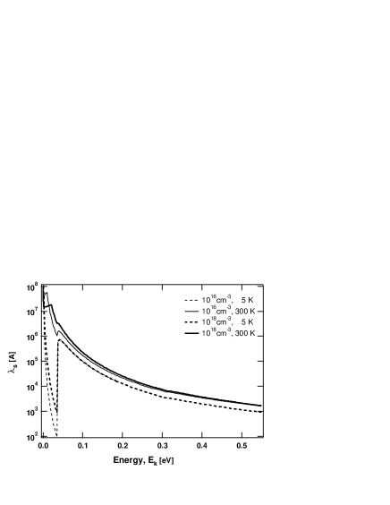
for electrons injected into GaAs and GaN, as a function of dopant density and electron temperature. They are then used to calculate spin relaxation times limited by EY, DP, and BAP mechanisms.9 The spin scattering lifetimes by EY and BAP are proportional to the momentum scattering lifetime. Interestingly, in the states with shorter momentum scattering times, the electrons do not stay long enough for spin to precess, resulting in longer relaxation times for spin scattering by DP mechanism. At very low injection energies ( 10 meV), the leading spin scattering is by EY (in n-doped) and BAP (in p-doped) material. However the p-doping must be at least 5 1017 cm-3 in GaN and 1 1018 cm-3 in GaAs for spin scattering by BAP to be comparable to that by EY. At higher energies, DP is the strongest mechanism for spin scattering in both GaAs and GaN. As the energy of the electrons is increased, the DOS available for scattering also increases. However, the momentum scattering rate decreases as k2 (for phonon scattering) and k4 (for impurity scattering). Consequently, the momentum scattering time increases with energy initially, then falls steeply once the threshold for phonon emission is reached. At even higher energy, the increase in DOS nearly compensates the decrease in the matrix element, resulting in a nearly-constant momentum relaxation time. The DP mechanism limited spin relaxation time , which varies as /E, decreases for increased energy but reaches a local peak at the threshold energy for phonon emission. The product of and the group velocity, , at that energy gives the energy-dependent mean free path, for the electrons. The calculated spin mean free path, , as a function of injection energy is plotted for two donor doping concentrations and temperatures in Fig. 1 and Fig. 2 for GaAs and GaN respectively. For all energies above 10 meV, DP mechanism is dominant, and consequently, we see that spin scattering lifetimes are longer at higher temperature and higher doping density where momentum scattering life-
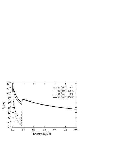
times are shorter. Also, the mean free path decreases rapidly with energy and reaches a local maximum at energy slightly above the LO phonon energy. Notice that mean free path of electrons with one LO energy is about 0.1 cm in GaAs and 1 cm in GaN. The longer mean free path of the injected electrons in GaN is primarily attributed to the small SO splitting (12 meV in GaN and 341 meV in GaAs), large band gap (of 3.4 eV in GaN and 1.5 eV in GaAs), and large DOS (effective mass of 0.2 m0 in GaN and 0.067 m0 in GaAs). At higher energies, the mean free path continues to decrease in spite of the increase in group velocity.
To determine the temperature dependence of the spin lifetime, a Fermi- Dirac distribution can be safely assumed because the phonon-limited momentum relaxation times ( 50 ps at 5K in GaAs) is typically two orders of magnitude shorter than the time scale of the spin relaxation times (s). An ionization energy for the donors in GaAs of 5.8 meV is used, a value commensurate with the SiGa defect.17 As the lattice temperature is reduced, fewer impurities are ionized, and the Fermi level (FL) is self-consistently obtained. An photo generated carrier density typically used in experiments,22 1014 cm-3, was added so that these results can be directly compared to Ref. 2. This last assumption only affects the low temperature ( 10 K) result due to carrier freeze-out. Figure 3 shows the results obtained for GaAs and GaN. The calculated energy-dependent spin relaxation lifetimes can be used to compare with the measured lifetimes at low or zero magnetic field. Figure 3 compares the averaged spin lifetimes (solid lines) and the experimental values2 (dashed-dots) in the temperature range of 5 K to 145 K. We see that the predicted trend (and slope) is in good agreement with experiment, except at very low temperature (10 K). For T 10 K, the absolute value of the calculated values are a factor of 2 to 3 smaller than experiment. At very low temperatures, the predicted lifetime decreases with T, whereas the measured lifetime appears

to reach a plateau. This difference may result from the presence of compensating defects in the experimental samples. The dopant density and low field mobility of the GaAs, reported in Ref. 2 at room temperature are 1016 cm-3 and 5400 cm2/v.s, respectively. Our calculations predict a mobility of 7100 cm2/v.s, in agreement with the values found for high purity samples.16 The lower mobilities measured in the experiment indicate that defects are present in the samples. The defect states would be expected to influence the FL and scattering times, particularly at low temperatures.
Assuming 5.8 meV of donor ionization energy for Si in zinc-blende GaN, the averaged spin lifetime calculations are carried out, and the values are also shown in Figure 3 (thick solid line). It is interesting to note the spin lifetimes in GaN are expected to be about three orders of magnitude larger than those in GaAs. The predicted enhancement is because of the combination of the dominance by DP mechanism, larger momentum scattering and smaller SO interaction. However, when the defect density is large, the defect-assisted EY mechanism which is dominant at low temperatures, severely limits the spin lifetimes. This is in agreement with the recent results in highly impure (with 5 108 cm-2) wurtzite-GaN where the measured lifetimes are an order of magnitude smaller than that in GaAs at T 50K.17 When the material quality is improved18-20 for much lower defect density (), a large increase in spin lifetimes is expected.
In summary, we have calculated the energy and temperature dependent spin lifetimes of electrons using full band structures of GaAs and GaN. The calculated spin lifetimes of low kinetic-energy electrons in GaAs are in reasonable agreement with measured values.2 We predict the spin lifetimes to decrease sharply with electron energy and reach a local maximum near one LO phonon energy at low T. In addition, because of the large conduction band DOS and smaller SO in GaN, the spin lifetimes are predicted to be three orders of magnitude longer than that in GaAs. When non-radiative recombination is not dominant, the mean free path for the electrons with an injected energy of 0.5 eV is predicted to be about 1 mm in high-purity GaN, suggesting GaN as more suitable materials for spin injection devices. The accuracy of the model will be enhanced by using parameter-free calculations in which the SO coupling is included in the Hamiltonian, and all other scattering processes (electron-phonon, electron-impurity) are considered as perturbations. Such calculations are in progress.
One of the authors (S.K) thanks Marcy Berding, Arden Sher, and Michael Flatte for useful discussions and Jay Kikkawa for providing the spin lifetimes data. This work was supported by the DARPA. (ONR contract # N00014-02-1-0598).
REFERENCES
- [1] S.A. Wolf, D.D. Awschalom, R.A. Buhrman, J.M. Daughton, S. von Molnar, M. Roukes, A.Y. Chtchelkanova, and D.M. Treger, Science, 294, 1488 (2001).
- [2] J.M. Kikkawa and D.D. Awschalom, Phys. Rev. Lett., 80, 4313 (1998).
- [3] R. Fiedrling, M. Keim, G. reuscher, W. Ossau, D. Schmidt, A. Waag, and L.W. Molenkemp, Nature, 402 787 (1999).
- [4] Y. Ohno, D.K. Young, B. Beschoten, F. Matsukura, H. Ohno, and D.D. Awschalom, Nature, 402 790 (1999).
- [5] B.T. Yonker, Y.D. Park, B.R. Bennett, H.D. Cheong, G. Kioseoglou, and A. Petrou, Phys. Rev. B62, 8180 (2000).
- [6] M.I. D’yakonov and V.I. Perel, Sov. Phys. JETP 33, 1053 (1971).
- [7] Y. Yafet, Solid State Physics, Ed. F. Seitz and D. Turnball (Academic, New York, 1963), 14, 1.
- [8] G.L. Bir, A.G. Aronov, and G.E. Pikus, Sov. Phys. JETP 42, 705 (1976).
- [9] G.E. Pikus and A.N. Titkov, Optical Orientation, Ed. F. Meier and B.P.Zakharchenya, (North-Holland, New York, 1984), Ch. 3.
- [10] P.H.Song and K.W.Kim, Phys. Rev. B66, 35207 (2002).
- [11] A.G. Aronov, G.E. Pikus, and A.N. Titkov, Sov. Phys. JETP 57, 680 (1983).
- [12] W.H. Lau, J.T. Olesberg, and M.E., Flatte, Phys. Rev. B 64, 161301 (2001).
- [13] A.-B. Chen and A. Sher, Semiconductor Alloys (Plenum, New York, 1996), Ch. 5 and 7.
- [14] S. Krishnamurthy, M. van Schilfgaarde, Appl. Phys. Lett. 71, 1999 (1997).
- [15] S. Krishnamurthy, A.-B. Chen, and A. Sher, Appl. Phys. Lett. 53, 1853 (1988).
- [16] S.M. Sze, Physics of Semiconductor Devices (John Wiley, New York, 1981) p. 21-29.
- [17] J.M. Kikkawa and D.D. Awschalom, Phys. Rev. Lett., 80, 4313 (1998).
- [18] A.!Sakai, H. Sunakawa, and A. Usai, Appl. Phys. Lett., 71, 2259 (1997).
- [19] S. Porowski, MRS International J. Nitride Semic. Res. 4S1, G1.3 (1999); MRS. Res. Symp. Proc. 449, 35 (1997).
- [20] Z.Y. Fan, G. Rong, N. Newman and D.J. Smith, Appl. Phys. Lett. 76, 1839 (2000).