Silicon-based molecular electronics
Abstract
Molecular electronics on silicon has distinct advantages over its metallic counterpart. We describe a theoretical formalism for transport through semiconductor-molecule heterostructures, combining a semi-empirical treatment of the bulk silicon bandstructure with a first-principles description of the molecular chemistry and its bonding with silicon. Using this method, we demonstrate that the presence of a semiconducting band-edge can lead to a novel molecular resonant tunneling diode (RTD) that shows negative differential resistance (NDR) when the molecular levels are driven by an STM potential into the semiconducting band-gap. The peaks appear for positive bias on a p-doped and negative for an n-doped substrate. Charging in these devices is compromised by the RTD action, allowing possible identification of several molecular highest occupied (HOMO) and lowest unoccupied (LUMO) levels. Recent experiments by Hersam et al. rHersamexpt support our theoretical predictions.
pacs:
PACS numbers: 05.10.Gg, 05.40.-a, 87.10.+eTraditionally molecular electronic efforts, both theoretical rtheory ; rDamle and experimental rReed ; rexpt ; rWeber ; rLindsay ; rReif , have been driven by thiol-gold chemistry to molecules bonded to gold substrates. However several recent experiments have demonstrated the feasibility of attaching various molecules on clean silicon surfaces rsiliconexpt . The development of molecular electronics on silicon is particularly important for two reasons. Firstly, it will enable the development of integrated devices that can utilize the powerful infrastructure provided by the silicon-based IC industry. Secondly, unlike gold, silicon has a bandgap that one can take advantage of to design a new class of resonant tunneling devices with possible applications in logic rFETlogic and low-power memory rmem . In view of these significant potential payoffs we believe it is worthwhile at this time to develop models that can be used to analyze the electrical characteristics of such silicon-based molecular devices.
The purpose of this paper is to present (i) a general formulation suitable for modeling silicon-based molecular devices; (ii) realistic principles for designing RTDs based on such structures; and (iii) showing ways to map out the molecular energy spectrum that is not realizable in normal experiments with gold contacts. Molecular devices on silicon require a formulation that can account for the bandgap, surface band-bending and surface reconstruction. One problem commonly encountered is that standard quantum chemical basis sets describe molecular energy levels well but provide a very poor description of the semiconductor bandstructure. We present a scheme that can be used to integrate the two distinct systems seamlessly and present results that combine ab initio treatments of the molecule with a semi-empirical description of the silicon bands. The same approach can be used to integrate the molecule with more advanced treatments of the silicon substrate.
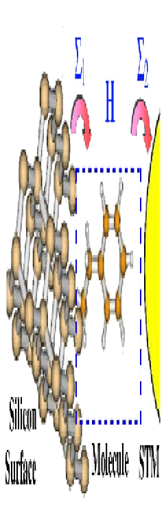
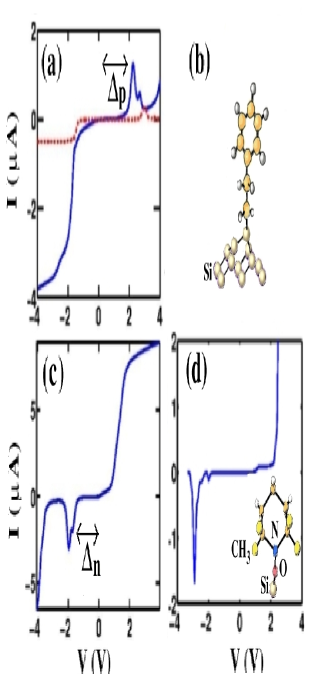
Our results show that we can expect to see NDR using molecules like styrene or TEMPO (2,2’,6,6’-tetramethyl-1-piperidynyloxy) on p-silicon at realistic positive substrate voltages, when current flow occurs through the HOMO levels. A schematic description is shown in Fig. 1. Recent experimental observations rHersamexpt are in good agreement with these results. By contrast, it appears that much larger negative voltages will be needed to observe these effects on n-type silicon where conduction takes place via the LUMO levels. This is an important observation that deserves careful attention, since little work has been reported to date for electronic conduction through the LUMO levels.
Formalism. We will use a method by which a bulk silicon bandstructure calculation (e.g. effective mass rlundu or tight-binding sp3s∗ rsp3s ) can be connected up with a detailed ab-initio treatment of the molecule, without introducing spurious basis-transformation related effects at their interface. We accomplish this connection through the real-space Green’s function obtained on a surface silicon atom, which can be looked upon both as a scooped-out part of the silicon crystal, as well as an extended part of the molecular device. The connection is established as:
| (1) |
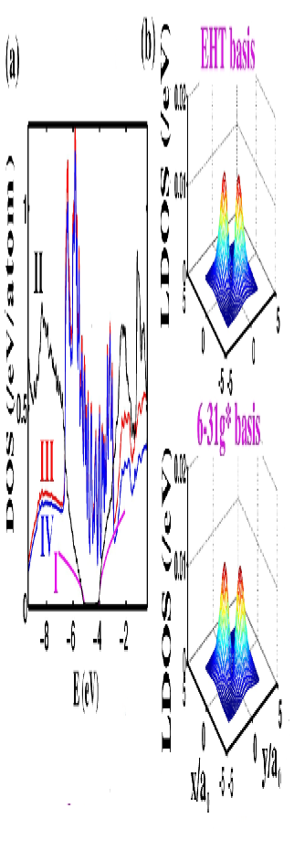
where and are the ab-initio overlap and Hamiltonian matrices for a surface silicon atom, is the desired self-energy coupling it to the bulk, and is the silicon surface Green’s function. We start with an appropriate semi-empirical description of the bulk silicon bandstructure, and use a real-space, recursive formalism along the (100) direction to get the semi-empirical surface Green’s function rManoj . We then use Eq. 1 to adjust the self-energy to achieve the best match between the surface Green’s functions (ab-initio and semi-empirical) in real-space (Fig. 2), including if required a suitable reconstructed cluster for unpassivated surfaces. We thus have an ab-initio description of the molecule and its bonding with the silicon surface that is consistent with a semi-empirical description of the bulk and surface properties of the silicon crystal rLAR .
We use a recently developed method rDamle ; rDamle2 to calculate the current, coupling the nonequilibrium Green’s function (NEGF) formulation of transport rDattabook with an LDA molecular Hamiltonian calculated using GAUSSIAN98 rGauss in a 6-31g∗ basis:
| (2) |
where are the molecular overlap and Hamiltonian matrices and are the contact Fermi energies. The calculated current includes contributions both from thermionic emission over the vacuum barrier, as well as quantum mechanical tunneling through it. We include the effects of an incoherent background inside the molecule through an additional phase-randomizing voltage-probe rButtiker , incorporated in the generalized Landauer-Büttiker formula rDattaSL .
It is well known rHoffman that unpassivated silicon has surface states in the band-gap, as we indeed observe (Fig. 2). Some of these states are eliminated once the molecule bonds to the surface silicon dimers rBond . The surface states in unpassivated silicon would influence the STM current only if they can be replenished from the bulk through inelastic processes occuring in the contact. We ignore such effects in this paper.
In any STM measurement on a molecule, it is important to deconvolve the tip and the molecular density of states (DOS) so that one can unambiguously identify features intrinsic to the molecule. Modeling tip-sample interactions requires a precise knowledge of the experimental tip structure, as well as its exact position over the molecule. It is generally believed rChen that the tunneling current drawn by a tungsten tip is dominated by the d-electrons of loose tungsten atoms at its end. We model the tip-sample interaction by evaluating the largest coupling matrix element between the styrene HOMO wavefunction and the d-electrons of a single tungsten atom sitting at varying distances from it. The coupling is obtained using LDA in a LANL2DZ basis, and yields a broadening 300 meV when the STM almost touches the molecule and 12 meV when the tip sits about 2 Å away. The STM self-energy is obtained using Fermi’s Golden rule, with a tip DOS eV. We find that the coupling can vary considerably depending on the lateral position of the tip atom relative to the molecule, due to accidental symmetries in the overlap matrix elements. This needs further consideration both from theory and experiment, given that the current level is influenced substantially by the STM tip.
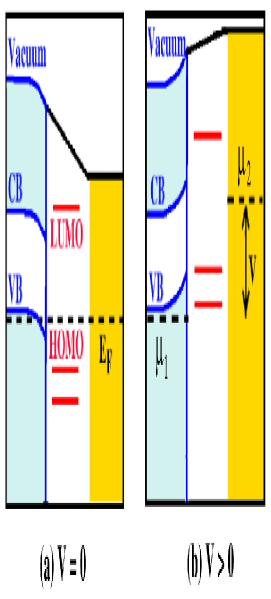
Much of molecular RTD action hinges on the bias-dependence of the molecular levels and broadenings. Using the semiconductor bulk band-edges as reference, the electronic energy levels and wavefunctions, the silicon band-bending, as well as the tip electrochemical potential vary under bias (Fig. 1). Under bias, the molecular levels move relative to the silicon band-edge, because (1) a large part of the applied bias drops across the tip-to-substrate gap due to the large dielectric constant of silicon relative to the molecule and the vacuum gap; and (2) the field inside the molecule is poorly screened by the absence of metal-induced gap states (MIGS) that would normally exist with gold contacts (this creates a low quantum capacitance which causes a sizeable potential drop within the molecule rparadigms ; rLiang ). At a critical voltage determined by the electrostatics, the HOMO level in Fig. 1 reaches the bulk silicon valence band-edge (VB) after which it enters the Si band-gap and its transmission drops abruptly, leading to a prominent NDR in the I-V of the molecule. Thus the self-consistent potential is the most important part of the modeling.
The equilibrium band-bending in silicon is given essentially by the workfunction difference between silicon and tungsten, and is distributed over a depletion width 1 nm. We obtain the voltage-dependence of the silicon band-bending using MEDICI rmedici , which agrees with simple estimates based on the depletion-width approximation rDW , as well as surface photovoltage (SPV) measurements rHamers . The band-bending affects the silicon surface Green’s function through the onsite energies of the silicon atoms distributed over a depletion width. Band-bending turns out however, to be relatively unimportant, since it is transparent to electron tunneling, so that the NDR is determined by the bulk silicon band-edges. The Laplace part of the potential drop is obtained using MEDICI rmedici by simulating a silicon surface separated from tungsten by a vacuum gap and a molecular dielectric with a dielectric constant 2. Stark effects in the molecular DOS are included in GAUSSIAN98 by applying a molecular field extracted from the Laplace potential.
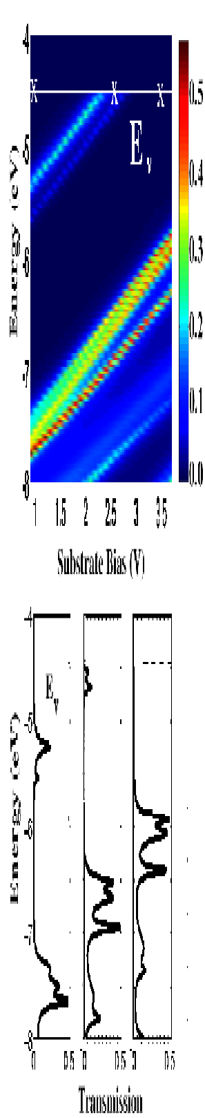
Results. Eq. 1 can be used to obtain the coupling of a molecule to silicon given a bonding geometry and a surface structure. The actual bonding geometries vary rMajor , and are sometimes controversial rbondgeom , so we will adopt specific models in this paper for illustrative purposes. We start by simulating transport through styrene grown on a p-doped ( cm-3) H-passivated Si(100) surface (bonding shown in Fig. 4b). Our LDA energy levels and wavefunctions of styrene agree well with previously published first-principles results for the above bonding geometry rWolkow2 . We use our hybrid basis scheme to connect this geometry to bulk silicon, described here within an effective mass model. The effective mass model is used for simplicity and describes the band-edge properties correctly (Fig. 2) where most of our physics lies; future publications rLAR will generalize this to more sophisticated models for bulk silicon. Fig. 3 shows a colorplot of the transmission of styrene on p-Si under bias. For increasing positive substrate voltage the molecular levels increase in energy until a HOMO level reaches the silicon valence band-edge and its transmission gets cut-off thereafter. This leads to an NDR in the I-V (Fig. 4a), calculated for an STM tip almost touching the molecule. The reduced transmission also leads to an overall current level that is much smaller for positive substrate bias. Multiple HOMO levels contribute to multiple NDR peaks. For negative bias, there is no such molecular NDR, since the HOMO levels move deeper into the valence band, and the LUMO levels lie outside the bias window. An increased tip-to-sample vacuum gap (2 Å) causes a smaller voltage drop across the molecule, postponing the onset of the NDR peaks (dashed line). The NDR peak position from a level is roughly given by , where denotes the average molecular potential under unit applied bias ( for an STM touching the molecule, decreasing approximately linearly with increasing vacuum gap).
For molecules on n-silicon, NDR is expected at negative substrate voltages, mediated through the LUMO levels. The LDA LUMO levels for styrene and TEMPO are a few volts higher than , pushing the first NDR peak outside the usual bias range. Fig. 4c shows the results for n-styrene, with the LUMO levels lowered artificially by about 1.5 eV. Electron addition levels are usually controversial, and could differ from theoretical predictions due to various effects associated with charging, correlation or image effects. The theoretical NDRs compare well with room temperature STM measurements by Hersam et al. rHersamexpt on TEMPO and styrene, both single molecules and monolayers. The experiments are performed on clean Si(100) surfaces, with a different surface reconstruction (2x1), bonding mechanism (cycloaddition), and bandbending rbandbb , but the corresponding theoretical results are qualitatively similar (Fig. 4d).
The origin of NDR in our simulations is qualitatively different from the NDR mediated by tunneling through localized atomic states arising from a sharp structure in the tip DOS rAvouris . NDR due to a tip to level resonance would show up either for both bias directions for both p and n-type samples (if the tip structure interacts with both HOMO and LUMO levels), or for one bias direction for only one of the samples (if it interacts with just one of them). The consistent observation of a one-sided NDR, at positive substrate bias in p-Si and negative in n-Si rHersamexpt , can only be explained by interactions between the molecular levels and the silicon band-edge.
The multiple NDR peaks arise from the multiplicity of levels sequentially crossing the relevant band-edge. This is a significant improvement over gold-based experiments, where large molecular charging energies ( 2 eV) prevent an STM electrochemical potential from crossing more than one level. So far, experimental molecular conductances exhibit very few (typically zero rLindsay , one rWeber ; rReif or two rReed ) peaks, in contrast to systems with smaller charging energies rBanin . In molecular RTDs, however, the proximity of the band-edge to the Fermi energy dramatically reduces this charging effect, because any charging due to electron/hole addition to a level by the stronger coupled substrate is counterbalanced almost instantly by its removal due to the dramatic reduction in substrate coupling at the bandedge. The low charging allows the observation of multiple NDR peaks that can be correlated with the molecular levels. Indeed, we can use a combination of p and n-type experiments on a single molecule to map out its HOMO-LUMO spectrum. For instance, the experimental peak voltages and Fermi energies for and -doped substrates give a HOMO-LUMO gap , including equilibrium tip-substrate band-alignment effects. Charging can also lead to a hysteresis in the I-V, associated with the changeover of the substrate coupling from strong to weak at the NDR position. Such hysteresis effects are observed in RTDs rRTDhyst , but will also be compromised by the low charging in these molecules. For realistic device parameters, the predicted hysteresis is small, and could be washed out by scattering.
We are grateful to M. Hersam and his group for liberally sharing their unpublished experimental results with us. In addition, we would like to thank M. S. Lundstrom, C-F. Huang, D. Janes and M. Paulsson for useful discussions. This work has been supported by ARO-DURINT, Award# 527826-02, NSF, Award# 0085516-EEC and by the Semiconductor Technology Focus Center on Materials, Structures and Devices under contract # 1720012625.
References
- (1) M. Hersam, private communications.
- (2) E. G. Emberly and G. Kirczenow, Phys. Rev. B 58, 10911 (1998); S. N. Yaliraki and M. A. Ratner, J. Chem. Phys. 109, 5036 (1998); J. Taylor, H. Guo and J. Wang, Phys. Rev. B 63, 245407 (2001); M. Di Ventra, S. T. Pantelides and N. D. Lang, Phys. Rev. Lett. 84, 979 (2000); J. J. Palacios, A. J. Pérez-Jiménez, E. Louis and J. A. Vergés, Phys. Rev. B 64, 115411 (2001); P. Damle, T. Rakshit, M. Paulsson and S. Datta, IEEE Trans. Nano. 1, 145 (2002); A. W. Ghosh, T. Rakshit and S. Datta, cond-mat/0212166.
- (3) P. S. Damle, A. W. Ghosh and S. Datta, Phys. Rev. B Rapid Comms. 64, 201403 R (2001).
- (4) M. A. Reed, C. Zhou, C. J. Muller, T. P. Burgin and J. M. Tour, Science 278, 252 (1997).
- (5) J. Chen, M. A. Reed, A. M. Rawlett and J. M. Tour, Science 286, 1550 (1999); D. Porath, A. Bezryadin, S. de Vries and C. Dekker, Nature 403, 635 (2000).
- (6) J. Reichert, R. Ochs, D. Beckmann, H. B. Weber, M. Mayor and H. v. Löhneysen, Phys. Rev. Lett. 88, 176804 (2002).
- (7) X. D. Cui, A. Primak, X. Zarate, J. Tomfohr, O. F. Sankey, A. L. Moore, T. A. Moore, D. Gust, G. Harris and S. M. Lindsay, Science 294, 571 (2001).
- (8) W. Tian, S. Datta, S. Hong, R. Reifenberger, J. I. Henderson and C. P. Kubiak, J. Chem. Phys. 109, 2874 (1998).
- (9) R. A. Wolkow, Jpn. J. Appl. Phys. 1 40, 4378 (2001); M. C. Hersam et al., Nanotechnology 11, 70 (2000); M. A. Reed (preprint).
- (10) R. H. Mathews, J. P. Sage, T. C. L. Gerhard Sollner, S. D. Calawa, C-L. Chen, L. J. Mahoney, P. A. Maki and K. M. Molvar, Proc. IEEE 87, 596 (1999).
- (11) Seabaugh et al., IEDM’98 Tech. Dig. pp. 429-432.
- (12) M. Lundstrom, “Fundamentals of carrier transport”, Cambridge University Press (2000).
- (13) Vogl et al. J. Phys. Chem. Solids 44, 365 (1983).
- (14) J. Cerda’ and F. Soria, Phys. Rev. B 61, 7965 (2000).
- (15) M. Samanta, Master’s thesis, Purdue University, 1999.
- (16) Detailed results for bulk and surface structures on silicon will be described in a forthcoming publication.
- (17) P. S. Damle, A. W. Ghosh and S. Datta, Chem. Phys. 281, 171 (2002), Special issue on Processes in Molecular Wires, ed. P. Hänggi, M. Ratner and S. Yaliraki.
- (18) S. Datta, “Electronic Transport in Mesoscopic Systems”, Cambridge University Press (1995).
- (19) H. B. Schlegel et al., GAUSSIAN98, Revision A.7. Gaussian, Inc., Pittsburgh, PA, 1998.
- (20) M. Büttiker, Phys. Rev. B 33, 3020 (1986).
- (21) S. Datta, Superlat. Microstruct. 28, 253 (2000).
- (22) Q. Liu and R. Hoffman, J. Am. Chem. Soc. 117, 4082 (1995); S. N. Molotkov, S. S. Nazin, I. S. Smirnova and V. V. Tatarskii, Surf. Sci. 259, 339 (1991); S. T. Pantelides and J. Pollman, J. Vac. Sci. Technol. 16, 1340 (1979).
- (23) R. J. Hamers, Ph. Avouris and F. Bozso, Phys. Rev. Lett. 59, 2071 (1987); R. Akiyama, T. Matsumoto and T. Kawai, Phys. Rev. B 62, 2034 (2000). (2000).
- (24) C. J. Chen, “Introduction to Scanning Tunneling Microscopy”, Oxford University Press (1993).
- (25) A. W. Ghosh and S. Datta, cond-mat/0303630.
- (26) G. C. Liang, A. W. Ghosh and S. Datta, unpublished.
- (27) Technology Modeling Associates, Inc., “TMA medici, two-dimensional device simulation program, version 4.0 user’s manual”, Sunnyvale, CA, 1997.
- (28) S. M. Sze, “Physics of Semiconductor Devices”, John Wiley and Sons (1983).
- (29) M. McEllistrem, G. Haase, D. Chen and R. J. Hamers, Phys. Rev. Lett. 70, 2471 (1993).
- (30) X.-Y. Zhu, V. Boiadjiev, J. A. Mulder, R. P. Hsung and R. C. Major, Langmuir 16, 6766 (2000).
- (31) S. K. Coulter, J. S. Hovis, M. D. Ellison and R. J. Hamers, J. Vac. Sci. Technol. A 18, 1965 (2000).
- (32) W. A. Hofer, A. J. Fisher, G. P. Lopinski and R. A. Wolkow, Chem. Phys. Lett. 365, 129 (2002).
- (33) The band-bending is constrained to lie between V by localized and dimer levels, as confirmed by SPV measurements (rHamers ). This makes it easier for the molecular levels to “slip” past the silicon surface bandedge, although it is the bulk bandedge that principally determines the NDR positions.
- (34) I-W. Lyo and P. Avouris, Science 245, 1369 (1989).
- (35) U. Banin, Y. Cao, D. Katz and O. Mello, Nature 400, 542 (1995).
- (36) H. L. Berkowitz and R. A. Lux, J. Vac. Sci. Technol. ¿ B 5, 967 (1987).