Now at ] Institute for Physical High Technology, P.O. Box 100239, D-07702 Jena, Germany
Conversion of phase-slip lines into elementary resistive domains in a current-carrying superconducting thin film
Abstract
A nonmonotonic dependence of the differential resistance of the first step of a phase-slip line on the heat-reservoir temperature near has been observed experimentally for the first time in a superconducting tin film. This behavior is interpreted as a conversion of the phase-slip line into an elementary resistive domain as the result of a deviation from the isothermal conditions.
pacs:
74.40.+k, 74.25.Qt, 74.78.Db, 74.50.+rThe mechanisms by which superconductivity is destroyed when a transport current is passed through a thin film are basically local mechanisms. Narrow films, whose width is smaller than the coherence length , stratify into so-called phase-slip centers in the process ivlev . In wide samples, an increase in the current is accompanied by a penetration of flux vortices from the edges of the film, near defects and irregularities. This effect results in a dissipation of energy and a local heating. Resistive regions or normal regions ( if the temperature rises to a value ) which are nonequilibrium and nonisothermal but nevertheless localized form ivanchenko ; yu . The current-voltage characteristic of such a film is stepped and has a substantial thermal hysteresis. If the heating is moderate ( , where is the heat-reservoir temperature), the film is unstable with respect to the formation of nonequilibrium, nearly isothermal regions of phase-slip lines: 2D analogs of phase-slip centers vol ; volotsk . The current-voltage characteristic of samples containing phase-slip lines is free of hysteresis and is stepped. It consists of a series of linear sections with differential resistances , . The resistance is determined by the resistance of the film in its normal state over a distance , where is the depth to which an electric field penetrates into the superconductor volotsk .
When elementary resistive domains ivanch form, the current-voltage characteristic may have qualitatively the same shape as for phase-slip lines. There is the distinction that the depth to which the electric field penetrates upon the formation of the elementary resistive domains is different, and it depends on the heating and the heat transfer. In addition, a thermal hysteresis appears on the current-voltage characteristic in the presence of an elementary resistive domain ivanch . The formation of elementary resistive domains experimentally is improbable. If the heat transfer is poor, one usually observes a coalescence of the elementary resistive domains into large domains. The smallest resistive domains which have been observed ivanch ; medvedev consist of six to ten elementary domains.

Phase-slip lines exist in only a narrow temperature interval volotsk , so neither the temperature dependence of the lines nor the changes caused in them by a deviation from isothermal conditions have previously been studied. In the present letter we are reporting a study of these questions.
The preparation of the samples consisted of the following steps: (1) vacuum deposition of tin to a thickness Å on silicon substrates; (2) photolithography to fabricate strips with a width m and a length mm; (3) the formation of a channel m wide and Å deep running across the strip, by electron-beam lithography and ion-beam etching. The lateral boundaries of the strip were modulated with an amplitude and a period of a few microns to facilitate the penetration of vortices. The channel served the same purpose. Experiments revealed that phase-slip lines could be observed even without the channel, but they were not as apparent in that case.
We recorded current-voltage characteristics of the samples, finding the temperature from the helium vapor pressure. Figure 1 shows a typical characteristic; it is what we would expect for phase-slip lines volotsk . There are linear regions of substantial width along the current scale; up to 20 distinct steps are observed. The resistance of the th step is , where is the resistance of the first step. As the temperature is lowered, this stepped structure persists, but a hysteresis appears.
We calculated the resistance of region KL in Fig. 1 from the slope of step , and we calculated the difference between the resistances of the second and first steps, , as functions of the reservoir temperature . The curves of and are not monotonic (Fig. 2). In interval , the points of the two plots coincide, and the positions of these points remain essentially unchanged as the temperature is cycled. Region has a significant scatter in resistances (Fig. 2).
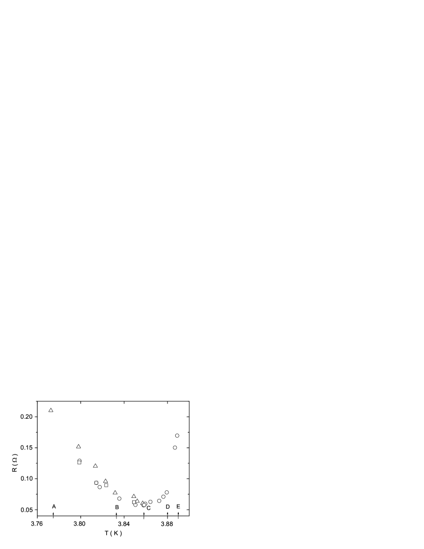
In region , which is close to , we do not yet have any phase-slip lines. In region there is a multitude of phase-slip lines.
For a quantitative analysis we use the expression ( volotsk , for example)
| (1) |
where is the resistivity of the film in the normal state, and
| (2) |
Here = / and we assume , since there is essentially no heating in interval ; we thus have
| (3) |
Here cm/s is the Fermi velocity, and s is the energy relaxation time for tin. The mean free path is usually found from the known value of . However, there is a substantial scatter in the values of this quantity in the literature, so we use the electron specific heat faber . We also use the expressions and , for the Ginzburg-Landau parameter gen , where is the London depth at . We thus find . Using the experimental value for our samples, we find Å. Correspondingly, we have m. Then we find
| (4) |
Here . Calculations yield .
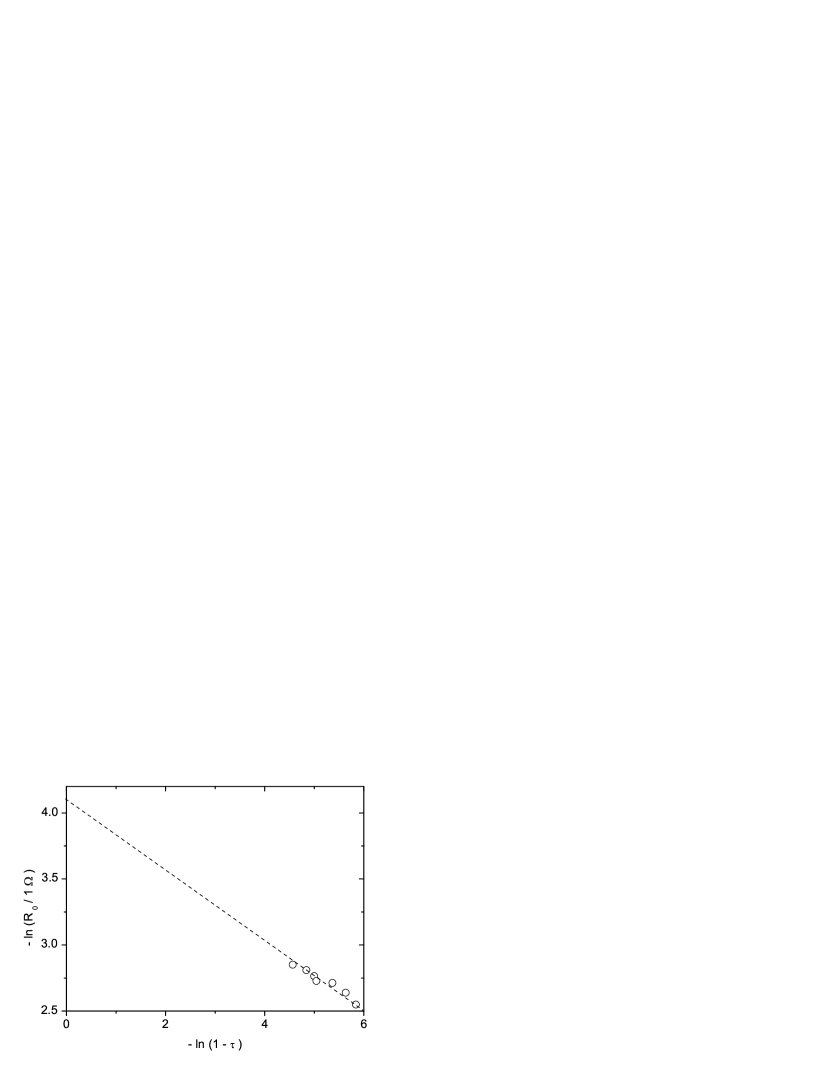
Figure 3 shows a plot of (1 ) (i.e., a dimensionless quantity) versus in logarithmic scale for temperature interval . The experimental points conform to a straight line with a slope . A continuation of this straight line intersects the resistance axis at the point , from which we find . The experimental results thus not only confirm functional dependence (4) but also agree quantitatively with it.
We know that resistive formations have two characteristic parameters: , the penetration depth of the electric field, and , the length scale of the temperature decay with distance from the center of the domain yu ; ivanch . The dependence of on the parameters of a sample was found in yu , but that dependence does not apply to our films, which have a good heat transfer. We will accordingly restrict our explanation of the behavior of the average differential resistance in region (Fig. 2) to a few qualitative comments. It is logical to suggest that the phase-slip lines become nonisothermal here and that thermal processes play a governing role. Specifically, (1) the hysteresis increase in interval ; (2) the steps on the current-voltage characteristic become noticeably nonlinear; (3) the resistance of the first step increases with decreasing temperature; and (4) estimates of for the case of a slight heating ( - ) in region show that is on the order of . This result means that deviations from an isothermal situation have a substantial influence on the size of the resistive formations. For estimates of here we used the expression , where is the thermal conductivity found from the Wiedemann-Franz law, and ) is the heat-transfer coefficient from neeper .
In region we are thus witnessing a transition from a phase-slip line to elementary resistive domains. In interval , thermal processes are determining the behavior of the current-voltage characteristic. Here the resistance and the current at which the first step appears depend on the temperature in roughly the same way; specifically, they are proportional to . It follows that the average differential resistance is linear in the current. The increase in the resistance in this temperature interval is probably due to a growth of the domain, whose size is proportional to the current at which it appears.
References
- (1) B. N. Ivlev and N. B. Kopnin, Usp. Fiz. Nauk 142, 435 (1984) [Sov. Phys. Usp. 27, 206 (1984)].
- (2) Yu. M. Ivanchenko, P. N. Mikheenko, and V. F. Khirnyi, Zh. Eksp. Teor. Fiz. 80, 171 (1981) [Sov. Phys. JETP 53, 86 (1981)].
- (3) Yu. M. Ivanchenko and P. N. Mikheenko, Zh. Eksp. Teor. Fiz. 82,488 (1982) [Sov. Phys. JETP 55, 281 (1982)].
- (4) V. G. Volotskaya, I. M. Dmitrenko, L. E. Musienko, and A. G. Sivakov, Fiz. Nizk. Temp. 7, 383 (1981) [Sov. J. Low Temp. Phys. 7, 188 (1981)].
- (5) V. G. Volotskaya, I. M. Dmitrenko, L. E. Musienko, and A. G. Sivakov, Fiz. Nizk. Temp. 10, 347 (1984) [Sov. J. Low Temp. Phys. 10, 179 (1984)].
- (6) Yu. M. Ivanchenko and P. N. Mikheenko, Zh. Eksp. Teor. Fiz. 83, 684 (1982) [Sov. Phys. JETP 56, 380 (1982)].
- (7) Yu. V. Medvedev and V. F. Khirnyi, Fiz. Tverd. Tela (Leningrad) 26, 1163 (1984) [Sov. Phys. Solid State 26, 705 (1984)].
- (8) Faber and A. B. Pippard, Proc. R. Soc. London 231, 336 (1955).
- (9) P. G. de Gennes, Superconductivity of Metals and Alloys, Benjamin, Inc., New York, 1966.
- (10) D. A. Neeper and J. R. Dillinger, Phys. Rev. A 135, 1028 (1964).