Residual Resistance in a 2DES: A Phenomenological Approach.
Abstract
We consider a simple phenomenological model of a semiconductor with absolute negative conductance in a magnetic field. We find the form of the domains of the electric field and current which arise as a result of an instability of a uniform state. We show that in both Corbino disc and Hall bar samples the residual conductance and resistance are negative and exponentially small; they decrease exponentially with increasing length
I Introduction
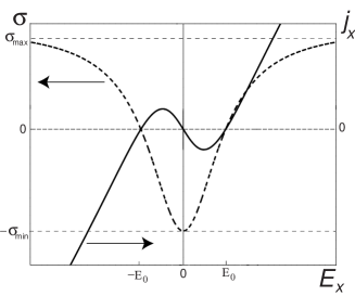
An interesting effect recently observed is that the resistance of a microwave irradiated two dimensional system (2DES) in a magnetic field drops almost to zero in certain intervals of [1, 3]. In magnetic fields too low for the observation of Shubnikov-de Haas oscillations () the resistance of a 2DES with mobility begins to oscillate in the presence of microwave irradiation [2]. In samples with higher mobility ( the resistance oscillations become more pronounced and the resistance drops almost to zero in some intervals of [1, 3] lower than the fields at which Shubnikov-de Haas oscillations begin to appear. Sometimes the states of the 2DES with almost zero resistance are called the zero resistance state (ZRS). These states have been observed in experiments on Hall bars [3, 1]. Similar measurements have been recently carried out on Corbino discs [4]. In this case a zero conductance state rather than the ZRS has been observed in the same intervals of the applied magnetic field . These experiments have drawn considerable attention, and during a short period of time many papers appeared where possible mechanisms for the observed effects were suggested [5, 6, 7, 8, 9, 10, 11, 12, 13, 14, 15, 16]. The most adequate mechanism seems to be the one based on the idea of absolute negative conductance (ANC) [6, 7, 8, 9, 10, 12, 13, 15, 16]. It was shown that a microwave irradiated 2DES in a strong magnetic field ( where is the cyclotron frequency, is the momentum relaxation time) may have absolute negative conductance . In some papers the calculations were carried out for a small bias electric field (a linear response). In Refs. [7, 16] the dependence was discussed and the conclusion was made that the dependence of on may have a N-shape form (see Fig.1). The authors of Ref. [8] assumed that the function has the N-shape form and showed that the states with negative differential conductance (NDC) are unstable with respect to small perturbations. As a result of this instability, a nonuniform distribution of the current density is assumed to arise and current domains (or current filaments) should appear in the sample. In this state the field is zero and a change in the total current leads for example to an enlargement of the domain with positive current and to a shrinking of the domain with negative current (the ZRS).
The possibility of a microwave induced ANC in semiconductors in a quantizing magnetic field was suggested and discussed some decades ago [24, 25, 26]. Around the same time phenomena in semiconductors with N- and S-shape characteristic were studied inensively both experimentally and theoretically (see the review article [18] and the book [19] and references therein). In particiular, it was shown that in semiconductors with the N-shape characteristic generally speaking moving domains of the electric field arise as a result of the instability of a state with the NDC. In semiconductors with the S-shape characteristics, domains (filaments) of the current density arise as a result of the instability. In the presence of the electric or current domains the characteristic changes drastically. In the first case an almost horizontal section appears on the characteristics (zero differential conductance), whereas an almost vertical section appears on the curve in the second case (zero differential resistance). If a system with S- or N-shape characteristic is placed in a magnetic field, the situation becomes more complicated: the form of the curve now depends on the measurement geometry (Hall bar or Corbino disc) [12] and both electric field and current domains may coexist. For example, if one assumes the N-shape form for dependence on in a Corbino disc (), then in the Hall bar measurements with increasing magnetic field the dependence acquires a complicated form becoming S-shaped at [12].
Strictly speaking, equations for macroscopic parameters (electric field, electron density etc) corresponding to experimental samples [1, 3, 4] are not yet derived. In the recent paper [16] a kinetic equation for the distribution function is derived which, in principle, could be applied to describe nonhomogeneous states. However this task is very difficult. All previous publications on these nonhomogeneous states are based on equations for macroscopic parameters. Therefore, although the dependence of the ZRS or ZCS on the applied magnetic field obtained theoretically [6, 7] qualitatively agrees with experimental results [1, 3, 4], it is difficult to convincingly conclude that the observed ZRS or ZCS are the result of instability of an uniform state in the 2DES with the S- or N-shape curve. Nevertheless even a phenomenological model of the S- or N-shape characteristics allows one to make certain conclusions about the observed curves. In this paper we admit a phenomenological model assuming a N-shape curve in the Corbino disc geometry and calculate the residual resistance (Hall bar experiments) or conductance (Corbino disc experiments). We show that in our model this resistance (conductance) depends exponentially on the ratio of the width of the sample to the width of the domain wall. Although our model does not correspond to the parameters of the real samples used in experiments [1, 3, 4], it has a physical meaning and allows us to make general statements about the stability of the system, the form of electric and current domains and the residual resistance of the system in a nonuniform state. In particular using model one can answer the question whether the state observed in experiments is dissipationless (as it happens in superconductivity and was anticipated in Ref.[1]) or not.
II Model
As in Ref.[12], we assume that depends on the electric field so that in the absence of (the Corbino disc) the dependence on has an N-shape form (see Fig.1). Such a dependence was discussed in Ref.[7](see also [16]). For example, this dependence may be obtained if we take for the expression
| (1) |
where is the conductance in strong fields (), and equals zero at the field The electric field as well as the conductivity should be determined from a microscopic theory (see Refs.[7, 16] and [17]). For example, according to Ref.[17] on the order of magnitude . In order to describe the form of domains, one has to know a microscopic mechanism which determines the form of the curve. For example in Refs.[18, 23] a superheating mechanism of the S-shape current-voltage characteristic was considered. In this case the width of the current domains is determined by the energy relaxation length. We assume that in our model a characteristic length is determined by the screening length (such a model was used to describe the Gunn effect [18, 19]). Therefore the current density can be written as
| (2) |
where is the conductivity tensor with diagonal components equal to and off-diagonal ones equal to , is the diffusion coefficient tensor which has a similar structure. The last term is the displacement current. We assume that only depends on the field . The components and are assumed to be independent of . At first glance the assumption about independence of the diffusion coefficient on violates the Einstein relation between the mobility and diffusion constant. However this relation holds only for systems in equilibrium. This is not the case for the system under consideration. Of course the diffusion coefficient depends on in some (unknown in our phenomenological appoach) way. This dependence can be taken into account if we introduce a new ”potential” in Eq.(6) or a new electric field. Therefore a corresponding analysis for the case of the energy dependent diffusion coefficient can be carried out in a similar way as for the constant For simlicity we ignore this dependence because it does not lead to qualitatively new results. Note that an analogous problem was discussed in the theory of the Gunn effect (see the reviews [18, 19] and references therein).
The electron concentration is related to the electric field via the Poisson equation (instead of -e we write +e making a proper choice of the electric field direction)
| (3) |
We also assume that the thickness of the 2DES is larger (or of the order) than the screening length . In this case in order to find a relation between and , one has to solve Eq.(3) inside the sample. Otherwise one has to solve an equation for the electric field (or potential) outside the sample taking into account corresponding boundary conditions. In the case Eqs.(2,3) yield correct results at least qualitatively. The main drawback of our model is the assumption of a local relationship between the current density and electric field which is true if the mean free path is shorter than a characteristic length of the problem (in our case the screening length). In the experiments one has the opposite relationship between and
III The Corbino disc
Let us consider first the simplest case of the Corbino disc geometry when (see Fig.2a).

| (4) |
| (5) |
These equations practically coincide with equations used in the theory of the Gunn effect [18, 19]. Linearizing these equations with respect to small fluctuations , one can easily show that states with negative differential conductance are unstable: where is the characteristic in an uniform case. This dispersion relation shows that the states with negative differential conductance are unstable with respect to long-wave perturbations. The characteristic length of the problem (the width of a domain wall) is determined by the relation: , where is the differential conductance. The conclusion on the instability of the states with a negative differential conductance was made a long time ago (see Refs [20, 21, 22]). As a result of the instability, domains of the electric field (in the x-direction) arise in the sample. In the y-direction these domains may be regarded as the current density filaments: different Hall currents flow in domains with opposite directions of the electric fields. In order to find the form of the domains of the electric field , we exclude from Eqs.(2,3) and arrive at the equation
| (6) |
Here is the normalised electric field, , is the characteristic screening length, , , . The ”potential” is defined as
| (7) |
where is the normalised bias current, is the normalised curve (see Fig.1). The electron density in an uniform case is the 3-dimensional electron concentration: it is related to the 2-dimensional density via , where is the thickness of the 2DES. We neglect the last term in Eq.(6) assuming that is small. Let us estimate for the samples used for example in the experiments [1, 3, 4]: for , we get , where . Obviously the field is much smaller than the very large value of . To find the form of stationary domains of the electric field, we neglect the last term in Eq.(6). In the following the analysis is similar to that presented in Ref. [18]. We integrate Eq.(6) and obtain the ”energy” conservation law which describes the phase trajectories
| (8) |
The integration constant determines the phase trajectory (see Fig.3). Its choice depends on concrete boundary conditions. We assume that at the boundaries the spatial derivates is zero (the final result does not depend qualitatively on particular boundary conditions). We are interested in a solution of the form of two domains with opposite electric fields. The field is connected with the length of the sample by the relation
| (9) |
where is the distance between the outer and inner radious of the Corbino disc. The constant is connected with by the equation
| (10) |
Our goal is to find a relation between the averaged field in the sample with the bias current The relation is the form of the current-voltage characteristic in the presence of domains. The averaged field is given by
| (11) |
The equations (9,10,11) determines the characteristic, or the residual conductance in the presence of domains. The function in these equations is shown in Fig.3 (solid line). It is clear that if the characteristic width of the domain wall (in our model ) is much less than the length , the trajectory should be close to the dash-dotted trajectory (the soliton trajectory). We calculate the residual conductance assuming that . In this case the fields inside domains are close to , the normalised bias current is very small and in the main approximation the integrals in equations (9,10,11) can be calculated analytically. Taking this into account, we find from Eqs.(9,10,11)
| (12) |
| (13) |
| (14) |
Here , Note that in our model the average field is positive if the bias current is negative, i.e. the resudial conductance is negative. We calculate the residual conductance in the limit of small currents If the condition
| (15) |
| (16) |
| (17) |
| (18) |
Therefore the residual conductance has the form (we restore the dimensional units)
| (19) |
We see that as well as are exponentially small. Therefore the assumed smallness of is justified. The formula (19) is valid if the condition (15) is fulfilled. This condition can be represented in the form
| (20) |
The formula (19) shows that the residual conductance is small (we assumed that ) and exponentially decreases with increasing length . Note that in a model more appropriate to the real experimements [3, 1] the characteristic length might differ from the screening length . If exceeds the value of the characteristic field in the rhs of Eq.(20), the residual conductance increases exponentially. Note that the obtained nonhomogeneous state with a negative differential conductance is stable if the total voltage is fixed (see Ref.[18]).
IV The Hall bar
In this Section we consider the case of the Hall bar geometry (see Fig.2b). In this case we have to write the equations for the currents having in mind that all quantities depend on
| (21) |
| (22) |
Taking into account the Poisson equation (3) and the fact that we obtain
| (23) |
| (24) |
Here is the bias current density which depends on , The conductivity because we assume that , and therefore As before we neglect small terms of the order The form of domains is determined by Eq.(24) that coincides with Eq.(6) if the latter small term in Eq.(6) is neglected. We note the electric field component does not depend on (this follows from the Maxwell equation in the stationary state which we are interested in: ). The current is -dependent; it has opposite directions in different electric domains. Our aim is to find a relation between the average current and the electric field , or the inverse relation From Eq.(23) we find
| (25) |
Calculating a relation between and from Eq.(24), as we did in the previous Section, we get
| (26) |
| (27) |
This result means that the residual resistance is equal to i.e., the residual resistance also is exponentially small in the Hall bar samples measurements. Note that in the expression for (19) the length should be replaced by The characteristics for a 2DES with two current (electric field) domains is shown in Fig.3 of Ref.[12].
V Conclusions
Using a simple phenomenological model, we have calculated the residual conductance (resistance) of a 2DES. We have shown that in measurements on both the Corbino disc and the Hall bar the residual conductance and resistance are exponentially small; they decrease exponentially with increasing length In our model the residual conductance and resistance are negative. A direct comparision of our results to experimental data meets difficulties because, as we mentioned before, parameters of the model do not correspond to real samples. Nevertheless one can note that the observation of a small negative resistance was observed in Ref.[27]. It would be of interest to measure the dependence of (in Hall bars) or (in Corbino discs) on the length or . This can shed light on the applicability of a model based on the negative conductance to the phenomenon observed in the experiments [1, 3, 4].
Note that we considered a limiting case . For an arbitrary ratio a linear analysis of the superheating instability in semiconductors with the S- or N shape I(V) characteristics has been carried out by Kogan [30]. It was shown that, as it happens in plasma [31], the superheating instability results in the appearance of oblique current filaments (electric field domains). Only in the limit these filaments are parallel to the bias current. Analysis of oblique domains is much more difficult problem as one needs to solve nonlinear equations in two dimensions with corresponding boundary conditions. It is clear however that if the voltage difference is measured between peripheral contacts, the Hall voltage also contributes to in the case of oblique domains. Since changes sign with changing the magnetic field direction, the voltage also can change sign. Therefore the contribution of the Hall voltage to might be a reason of the sign change of with changing the magnetic field direction observed in recent experiments [27].
Note added: After the preparation of this manuscript [28] we became aware of Ref.[29] in which similar ideas were elaborated.
REFERENCES
- [1] R.G.Mani, J.H. Smet, K. von Klitzing, V. Narayanmurti, W.B. Jonson, V. Umansky, Nature 420, 646 (2002).
- [2] M.A. Zudov, R.R. Du, L.N. Pfeiffer, and K.W. West, Phys.Rev.Lett. 90, 046807 (2003).
- [3] M.A. Zudov, R.R. Du, J.A. Simmons, and L. Reno, Phys.Rev. B 64, R201311 (2001).
- [4] C.L. Yang, M.A. Zudov, T.A. Knuuttila, R.R. Du, L.N. Pfeiffer, and K.W. West, Phys.Rev.Lett. 91, 096803 (2003).
- [5] J.C.Phillips, cond-mat/0212416, 0303181; 0303184.
- [6] A.C. Durst, S. Sachdev, N. Read, and S.M. Girvin, Phys.Rev.Lett. 91, 086803 (2003)..
- [7] J.Shi and X.C. Xie, Phys.Rev.Lett. 91, 086801 (2003)
- [8] e A.V.Andreev, I.L. Aleiner, and A.J.Millis, Phys.Rev.Lett. 91, 056803 (2003)
- [9] P.W. Anderson and W.F. Brinkman, cond-mat/0302129.
- [10] A.A.Koulakov and M.E. Raikh, cond-mat/0302465.
- [11] S.A.Mikhailov, cond-mat/0303130.
- [12] F.S.Bergeret, B.Huckestein, and A.F.Volkov, Phys.Rev.B 67, 241303(R) (2003)
- [13] S.I.Dorozhkin, cond-mat/0304604.
- [14] I.A.Dmitriev, A.D.Mirlin, D.G.Polyakov, cond-mat/0304529.
- [15] V.Ryzhii and V.Vyurkov, cond-mat/0305199; cond-mat/0305454.
- [16] M.G.Vavilov and I.L.Aleiner, cond-mat/0305478).
- [17] V.Ryzhii and A.Satou, cond-mat/0306051
- [18] A.F. Volkov and Sh.M. Kogan, Sov.Phys. Uspekhi 11, 881 (1969).
- [19] V.L.Bonch-Bruevich, I.P.Zvyagin, and A.G.Mironov, Domain Electrical Instabilities in Semiconductors (Consultant Bureau, New York, 1975)
- [20] V.F.Elesin and E.A.Manykin, Sov. Phys. Solid State 8, 2891 (1967).
- [21] A.L.Zakharov, Sov.Phys.JETP 11, 478 (1960).
- [22] V.L.Bonch-Bruevich and Sh.M. Kogan, Sov. Phys. Solid State 7, 15 (1965).
- [23] A.F. Volkov and Sh.M. Kogan, Sov.Phys. JETP 25, 1095 (1967).
- [24] V.I.Ryzhii, Sov.Phys.Solid State 11, 2078 (1970); V.I.Ryzhii, R.A.Suris and B.S.Shchamkhalova, Sov.Phys.Semicond. 20, 1299 (1987).
- [25] V.F.Elesin, Sov.Phys. JETP 28, 410 (1969).
- [26] V.V. V’yurkov and P.V. Domnin, Sov.Phys. Semicond. 13, 1137 (1979).
- [27] R.Willett, L.N.Pfeiffer, and K.W.West, cond-mat/0308406 (2003).
- [28] A.F. Volkov and V.V. Pavlovskii, cond-mat. 0305562 ( May 23, 2003).
- [29] R.Klesse and F.Merz, cond-mat/0305492 (May 21, 2003).
- [30] Sh.M.Kogan, Sov.Phys. Solid State 10, 1213 (1968).
- [31] E.P.Velikhov and A.M.Dykhne, Comptes rendus de la VI Conf.internat. sur les phenomenes d’ionisation dans les gas. Paris, 2, 511 (1963)