Bias-voltage dependence of the magneto-resistance in ballistic vacuum tunneling: Theory and application to planar Co(0001) junctions
Abstract
Motivated by first-principles results for jellium and by surface-barrier shapes that are typically used in electron spectroscopies, the bias voltage in ballistic vacuum tunneling is treated in a heuristic manner. The presented approach leads in particular to a parameterization of the tunnel-barrier shape, while retaining a first-principles description of the electrodes. The proposed tunnel barriers are applied to Co(0001) planar tunnel junctions. Besides discussing main aspects of the present scheme, we focus in particular on the absence of the zero-bias anomaly in vacuum tunneling.
pacs:
72.25.Mk, 73.40.Gk, 75.47.JnI Introduction
At present, extensive efforts are undertaken to employ the electronic spin in ‘magneto-electronic’ devices. This aim challenges especially applied physics, but one is also concerned with model systems of spin-dependent transport in order to understand the basic phenomena. Maekawa and Shinjo (2002) Prototypical devices for studies of ballistic tunneling are planar tunnel junctions (PTJs), which consist of two magnetic electrodes separated by an insulating spacer. Of particular interest are the dependencies of the tunnel magneto-resistance (TMR) on the electronic structure of the leads and the spacer, on the width of the spacer, and on the bias voltage.
The conductance of a PTJ depends on the density of states (DOS) of the electrodes and of the tunneling probability of the scattering channels. Slonczewski (1989) The TMR can then be related to the spin polarization of the ferromagnetic electrodes. Jullière (1975) Biasing, which can be viewed as a shift of the chemical potential of one electrode relative to that of the other, enlarges the range of energies in which electrons can tunnel through the spacer and introduces an energy dependence of the electrode spin polarization.
State-of-the-art calculations for spin-dependent tunneling are based on the very successful density-functional theory (DFT). Gross and Dreizler (1995) A bias voltage, however, leads to a non-equilibrium state, which makes it difficult to apply DFT. An appropriate theoretical description of such a system would require non-equilibrium Green functions (see, e. g., Ref. Reiss, 1990). Therefore, a question arises how one can maintain the ab-initio framework of electronic-structure calculations, in particular for the leads, but treat the bias voltage in a feasible manner.
Focusing on spin-dependent ballistic tunneling through PTJs with finite bias, we investigate in the present work as a simple case tunneling through a vacuum barrier. The electronic properties of the electrodes from the spacer can still be computed within spin-polarized DFT. The crucial point is the electrostatic potential in the spacer region. Guided by first-principles calculations for jellium Lang (1992) and by theoretical models for surface barriers, we construct tunnel barriers that show the correct asymptotical behavior for large spacer thickness. In particular, one of them compares well with barrier shapes obtained ab initio for jellium. The absence of the zero-bias anomaly (ZBA) in vacuum tunneling of Co(0001) which was recently found by Ding and coworkers Wulfhekel et al. (2002); Ding et al. (2003) lends itself support for an application of the proposed tunnel barrier (for an experimental investigation of Co PTJs with an oxide barrier, see Ref. LeClair et al., 2002). We note in passing that the effect of interface states on vacuum tunneling in fcc-Co(001) was recently investigated theoretically. Wunnicke et al. (2002); Wang et al. (2003)
The paper is organized as follows. In Section II, two heuristic ways of constructing a tunnel barrier (II.2.2 and II.2.3) are motivated. Section II.3 deals with computational aspects of calculations for ballistic tunneling. Results for vacuum tunneling between Co(0001) electrodes are discussed in Section III.
II Theoretical
II.1 Surface-barrier shapes of metals
The shape of the surface barrier of a metal was investigated in a vast amount of publications. The possibility to calculate accurately reflected intensities in low-energy-electron diffraction (LEED), which is a particular surface-sensitive spectroscopy, led to several barrier models. Especially at very low energies (VLEED), the shape of the surface barrier has a considerable effect on the LEED spectra. McRae and Kane (1981) The free parameters that enter its functional description are fixed by fitting theoretical to experimental data, e. g., to VLEED intensities or to energies of surface and image-potential states. Chulkov et al. (1999) The latter can be accessed by inverse or by two-photon photoelectron spectroscopy. Graß et al. (1993) Note that electronic-structure calculations using the local-density approximation (LDA) do not reproduce the correct image potential in the vacuum.
Regarding electron diffraction, the classical electrostatic potential at a metal surface, with asymptotics , was first investigated by Mac Coll. Mac Coll (1939); Uni To avoid the divergence at the metal surface, Cutler and Gibbons Cutler and Gibbons (1958) proposed a model potential which interpolated between the (constant) inner potential of the metal and the image-charge potential in the vacuum region. Among the various proposed models, two became the most popular: the so-called JJJ barrier, named after the inventors Jones, Jennings, and Jepsen Jones et al. (1984) (see II.2.3 below), and the Rundgren-Malmström (RM) barrier Rundgren and Malmström (1977); Malmström and Rundgren (1980) (for a discussion of JJJ and RM barriers, see Ref. Graß et al., 1993). However, electron scattering is a dynamical process and these static shapes hold in principle only for the energy of interest. An energy-dependent generalization of the JJJ barrier suggested by Tamura and Feder proved to be successful in describing the image states at the Pd(110) surface. Tamura and Feder (1990) Further, the atomic structure at the surface leads to a corrugated (three-dimensional) surface potential. Tamura and Feder (1983); Lent and Kirkner (1990); Joly (1992); Henk et al. (1993); Lorenz et al. (1997) However, for most applications the laterally (one-dimensional) and energetically invariant shapes appear to be sufficient.
II.2 Construction of the tunnel barrier
In this Section, we propose two methods of constructing the tunnel barrier. The first method uses the electrostatic potential of a charge between two electrodes (II.2.2), the second approach is a simple superposition of surface potentials (II.2.3).
II.2.1 Electrostatic potential between two metal surfaces
Consider a planar tunnel junction with the lead occupying the half-space , whereas the lead fills , with (Fig. 1).
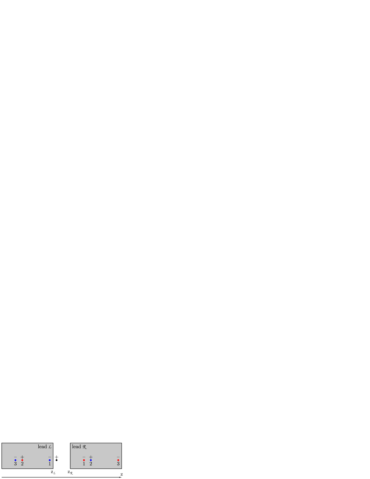
The electrostatic potential of a charge between the two semi-infinite metals can easily be obtained by the method of image charges. Uni Because each metal surface acts as mirror, one has to sum up two infinite series of image-charge potentials (blue and red circles in Fig. 1). This procedure results in
| (1) |
Here, is Euler’s constant and denotes the Digamma function. Abramowitz and Stegun (1970) The latter is the logarithmic derivative of the Gamma function , , with , for , and for . Obviously, diverges for and . It shows further the well-known asymptotics for the presence of a single metal. For example, expanding in a power series around yields
| (2) |
Considering only the first-order approximation for , i. e., the direct images of the charge (labeled in Fig. 1),
| (3) |
one sees that represents a higher barrier than because the images of even order produce an additional repulsion (‘’ in Fig. 1).
II.2.2 Image-charge potential as tunnel barrier
The electrostatic potential between two semi-infinite jellium metals including a bias voltage was calculated self-consistently within DFT by Lang. Lang (1992) He found that even with finite bias the potential in the electrodes is constant a few Bohr radii apart from the respective surfaces. Further, the divergence of the classical image-charge potential at and is bridged over by a smooth interpolating function which shows the form of a typical LEED-motivated surface barrier (cf. II.1). And last, application of a bias voltage apparently produces a linear potential drop in the spacer region (cf. Fig. 2b in Ref. Lang, 1992). Guided by these findings we construct in the following a tunnel barrier by means of the classical electrostatic potential [eq. (1)] and by LEED-type surface potentials.
To avoid the divergences of the electrostatic potential , a smooth continuous interpolating function between the image-charge potential and the inner potentials of the leads, and , is used (The vacuum energy is taken as energy zero). For this paper we choose a Lorentzian shape Henk et al. (1993) but any other reasonable shape can be used, too (see II.1). The interface potential then reads
| (4) |
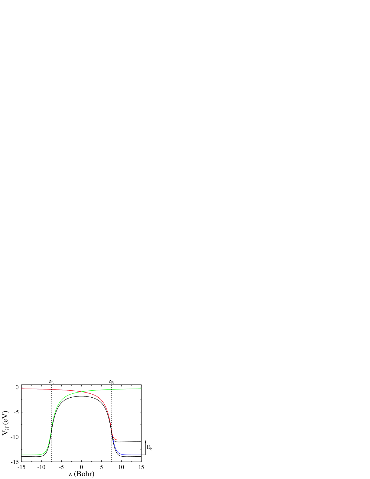
The coordinates , , and specify the positions of the onset of the interpolating Lorentzian, of the divergence of the potential , and of the transition to with respect to (Fig. 2).
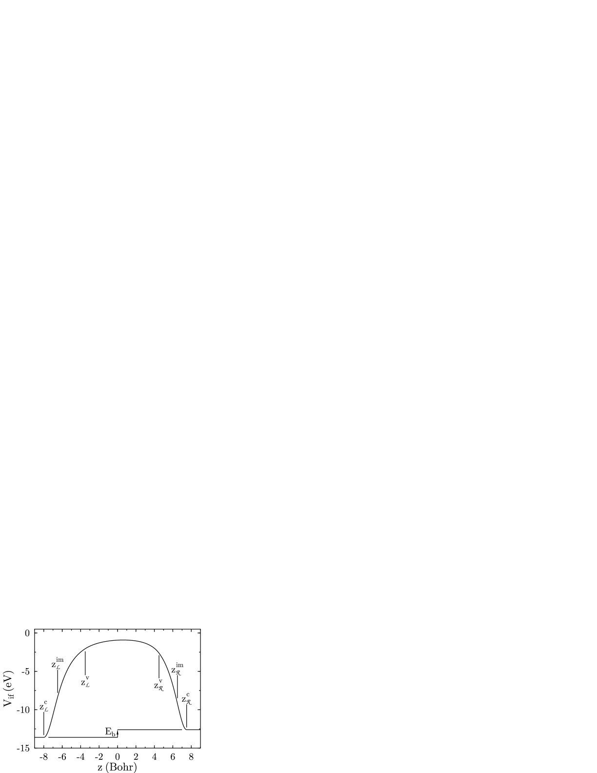
They have to be obtained by comparing theoretical results with other data, e. g., surface-state energies, VLEED spectra, etc, for the surface system (i. e., in the limit ). The parameters , , and are fixed by the conditions of smooth continuity in and . Analogous considerations apply for lead . The potential in the interior of the spacer can be chosen to incorporate the electrostatic potential between two metal electrodes, , and the bias voltage as well, as being discussed in the following.
Bringing two metals so close that electrons can tunnel from metal to the other aligns the Fermi levels of the two leads. This energy shift is given by the contact potential , i. e., the difference of the work functions of and of . Note that the alignment of the Fermi levels is accompanied by a shift of the inner potentials, that is, e. g., of the semi-infinite system is replaced by . Since was not specified explicitly in eq. (4), it can account for the contact potential and the bias voltage,
| (5) |
Here, is the electrostatic potential from eq. (1) and is the bias, for which a linear drop over the interface region is assumed:
| (6) |
This ansatz is motivated by the fact that the electric field is well screened within the electrodes but unscreened within the vacuum spacer.
Figure 3 presents a series of tunnel barriers in dependence of the lead separation .
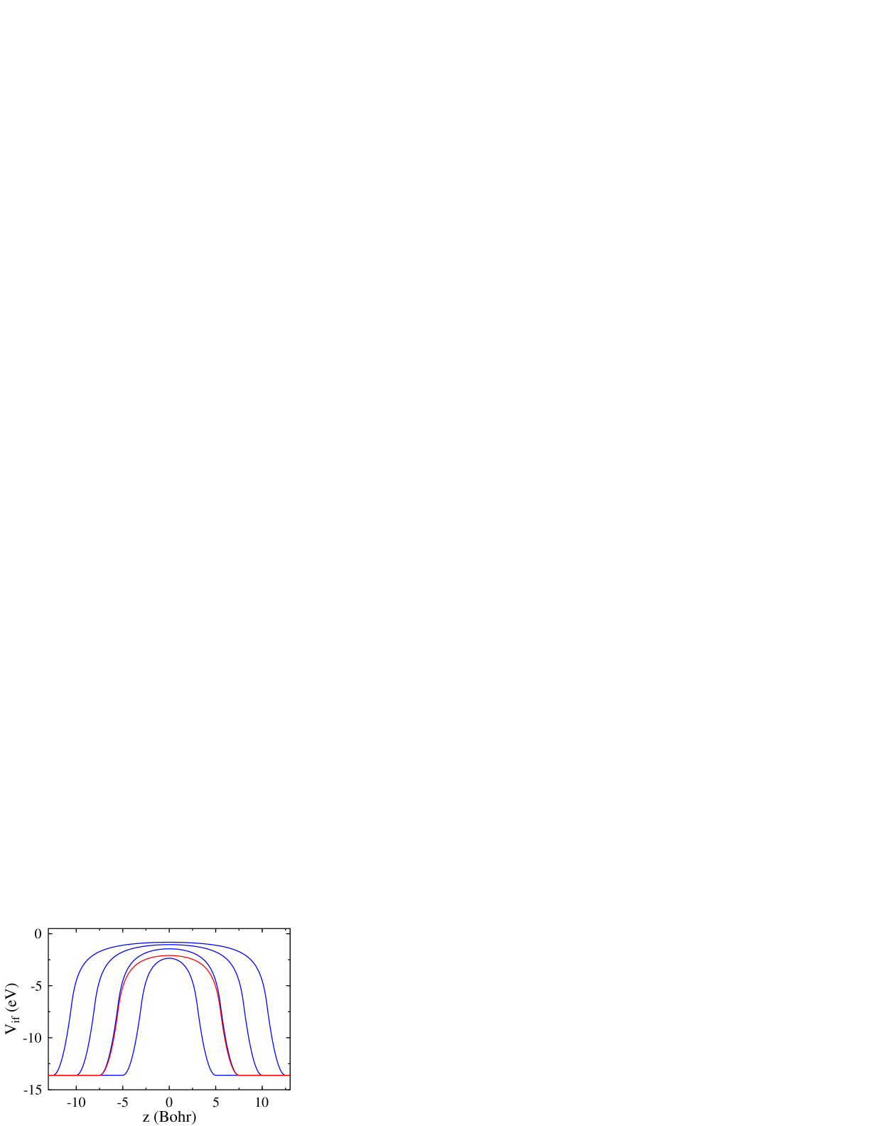
The heights of the barriers increase with separation (for an experimental estimation of the barrier height vs distance, see Ref. Wulfhekel et al., 2002). As already mentioned, taking the first-order approximation instead of leads to a reduced height (cf. the red line for 15 Bohr radii lead separation). The shape dependence on the bias is addressed in Fig. 4.
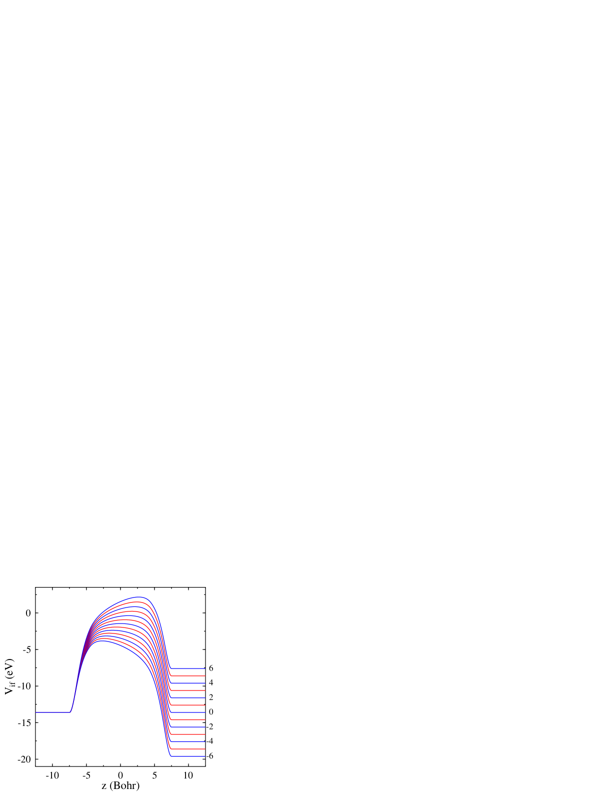
For rather large bias, the linear potential drop in the interface region can be clearly retrieved. We note in passing that the present construction produces potential shapes that compare qualitatively well with those obtained ab initio for jellium by Lang. Lang (1992) Further, a similar approach was recently used to explain the Stark shifts of surface states in scanning tunneling spectroscopy. Limot et al. (2003)
One advantage of the present approach is that the height of the tunnel barrier is automatically adjusted in dependence on the lead separation and on the bias voltage. Further, the barrier shape shows the correct image potential asymptotics for large lead separation [cf. eq. (3)]. In turn, the approach should not be applied for too small separations because the barrier shape would significantly differ from the interface potential which would be obtained from a self-consistent calculation for a narrow tunnel junction. This, however, could possibly be compensated by adjusting the parameters , …, not for the semi-infinite system but for the narrow junction.
II.2.3 Superposition of surface barriers
For large lead separations and small bias voltages, the probability of electrons to tunnel from one lead to the other is very small. Hence, in a self-consistent calculation for a tunnel junction, the tunnel barrier appears to be almost exclusively determined by the electron density of the respective lead and not significantly influenced by that of the other lead. This consideration might lead one to construct a tunnel barrier by superposition of the respective surface barriers,
| (7) |
where and are the surface potentials of the respective leads. Taking JJJ barriers, Jones et al. (1984) one arrives at
| (8) |
for the surface barrier of . The values of and are determined by requiring smooth continuity at . Because is known from the self-consistent calculation for the surface system, and remain as the only parameters to be adjusted. For the surface potential of one obtains an analogous form.
The simple superposition of surface barriers appears to be problematic for hetero-junctions or biased junctions. In both cases, the relative energy shift of one electrode, say , results in a finite potential which extends into the entire other electrode . This is due to the fact that the surface potential of extends infinitely far into . One way to overcome this problem is to take the bias only as an energy shift in the interior of , that is, to replace the inner potential by .
Figure 5 shows a superposition of JJJ surface barriers.
The inner potential of is shifted (cf. the arrow) by . Apparently, the barrier shape does not change significantly with bias in , in contrast to the former construction (Fig. 4). In particular, the linear potential drop is not observed.
II.2.4 Résumé
The two construction recipes result in tunneling barriers with different features. While the more elaborate one [eq. (4)] produces barrier shapes which are qualitatively close to those obtained from first-principles for jellium, Lang (1992) the barriers of the superposition approach [eq.(7)] lack most of these important features. In particular, the linear potential drop in the spacer region is missing. Both approaches can easily be extended to energy-dependent and corrugated (three-dimensional) tunnel barriers.
II.3 Computational aspects of ballistic tunneling
For the ballistic-tunneling calculations we applied the layer-KKR (Korringa-Kohn-Rostoker) approach of MacLaren and coworkers MacLaren et al. (1999) which is based on the Landauer-Büttiker result for the tunnel conductance. Büttiker (1986) At a given energy and in-plane crystal momentum , one computes the Bloch states and of the electrodes and and classifies them with respect to their propagation direction: to the right () or to the left (). The scattering matrix of the spacer is first computed in a plane-wave basis using LEED algorithms (like layer-doubling and layer-stacking; see for example Ref. Henk, 2001a) and subsequently expressed in terms of the scattering channels, i. e., in the Bloch-state basis. The transmission at the tunnel energy is then a sum over all pairs of Bloch states that are incident in and outgoing in ,
| (9) |
The tunnel conductance is obtained by summing over the two-dimensional Brillouin zone (2BZ),
| (10) |
Here, is the quantum of conductance which equals in atomic units. Uni Adaptive mesh refinement provides an efficient method to obtain accurate and well-converged 2BZ sums, in particular, if small parts of the 2BZ contribute significantly to the conductance. Henk (2001b)
With a bias voltage applied, electrons can tunnel from occupied states of one lead into unoccupied states of the other lead. The total conductance is then obtained by integrating over the energy interval given by the Fermi energies of the electrodes. The averaged conductance thus reads
| (11) |
The tunnel magneto-resistance (TMR) is defined as the asymmetry of the (averaged) conductances for parallel (P) and antiparallel (AP) alignment of the electrode magnetizations,
| (12) |
To treat in practice the bias voltage we proceed as follows. First, self-consistent electronic-structure calculations for the semi-infinite leads and generated muffin-tin (MT) potentials of the bulk, of the surface, and in the vacuum region. The MT zeroes were taken as inner potentials and , respectively (the MT zero is the constant potential in the interstitial region). For each of the leads, the MT potentials in the vacuum region were replaced by a smooth surface barrier. The parameters of the latter were fixed by requiring that the spectral densities in the surface layers were as close as possible to that of the original self-consistent calculation. Here, the focus laid in particular on the energy range used in the subsequent tunneling calculations and on surface states. For Co(0001), an important feature is the energy of the majority surface state at (cf. Fig. 2b in Ref. Ding et al., 2003; see also Refs. Math et al., 2001; Braun and Donath, 2002; Okuno et al., 2002).
Having fixed the barrier parameters, the tunnel junction was built from the bulk and surface potentials of the two electrodes and the interface barrier [eqs. (4), (5), and (6)]. The spacer comprises all layers with potentials that differ from the respective bulk potentials. In example, for a Co(0001) tunnel junction the first four layers on either side of the smooth tunnel barrier were used. The bias was taken into account by shifting the inner potential of one of the leads (muffin-tin zero) and determining the barrier shape [eq. (1)]. The smooth barrier was treated as a single layer in the multiple-scattering calculations. Its scattering matrix was obtained within the propagator formalism. Jepsen and Marcus (1971)
As usual for the KKR method, a small imaginary part has to be added to the energy , Weinberger (1990) leading in general to complex wavenumbers . Slater (1937); Heine (1963) Therefore, the electrode eigenfunctions are no longer true Bloch states but become evanescent states []. Eigenstates stemming from Bloch states [ for ] show typically the smallest and can therefore be separated from evanescent states [ for ]. MacLaren et al. (1999) In the spacer , the nonzero leads to damping in addition to the intrinsic one, artificially enhancing the decay of the conductance with spacer thickness. Further, the scattering matrix is no longer unitary and, hence, the total current is not conserved. Therefore, one has to choose carefully in order to produce reliable results. We found that a value of produces no considerable artefacts.
The Landauer-Büttiker approach used here avoids the computation of the Green function of the complete system, which is in particular problematic for a non-equilibrium system. Considering the asymptotic transmission channels (Bloch states), states that are localized at the barrier do not contribute to the transmission.
Recently, Davis and MacLaren reported on model calculations for spin-dependent tunneling at finite bias. Davis and MacLaren (2000) In their work, however, the electronic structure of the Fe electrodes was approximated by plane waves, whereas the barrier was assumed as step-like with a linear drop. Although conceptual similar, our approach goes beyond that work. First, the electrodes are treated on first-principles level. Second, the barrier shows the correct asymptotics (for the free surfaces) and, once the shape parameters being fixed, depends automatically on both lead separation and bias.
III Results for Co(0001)
Recently, Ding and coworkers investigated the bias-voltage dependence of the TMR with a spin-polarized scanning tunneling microscope (STM). Ding et al. (2003) In contrast to tunneling through oxide barriers, they observed no zero-bias anomaly (ZBA), i. e., a (rather) sharp maximum of the TMR at zero bias (see, for example, Ref. Yuasa et al., 2002). With a vacuum barrier replacing an oxide barrier, the TMR appeared to be almost constant. This finding suggests that the ZBA is mainly due to imperfections in oxide barriers, rather than to scattering at magnons and spin excitations (in the leads). Further, the so-called DOS effect, i. e., the energy dependence of the spin-resolved density of states of the leads, proved to be small in the case of Co(0001).
The experimental findings of Ding et al. were corroborated by ballistic tunneling calculations for planar Co(0001) junctions as sketched in Section II.3. The tunnel barrier was taken as a superposition of surface barriers (II.2.3). In the present work, we focus on the more elaborate image-charge potential (II.2.2).
The transmission , eq. (9), depends on the relative orientation of the lead magnetizations (P and AP), as is shown for bias (tunneling at ) in Fig. 6.
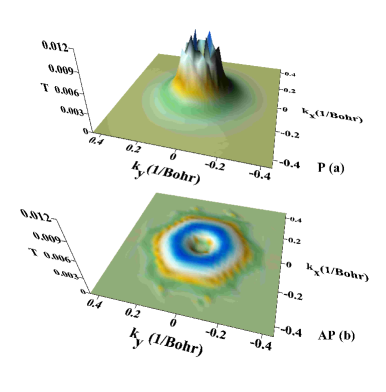
For the chosen lead separation of Å, only those Bloch states with a in the central part of the 2BZ contribute significantly to the transmission. The normal component of the wavevector within the tunnel barrier, , is imaginary and gives rise to strongly evanescent states in the tunnel barrier for Bloch states with large , and, thus, to a small transmission. For Bloch states with near (i. e., ), the decay within the barrier is less and the transmission can be larger. In total, this results in a ‘focusing’ of at the 2BZ center.
Both the P and the AP case show minor transmission close to . These minima are surrounded by ring-like structures of increased transmission. The maximum P transmission is larger than for AP alignment (by a factor of about ). But the AP transmission displays a broader ring compared to the P transmission.
When integrated over the 2BZ, one finds that (cf. the black symbols in Fig. 7 for zero bias).
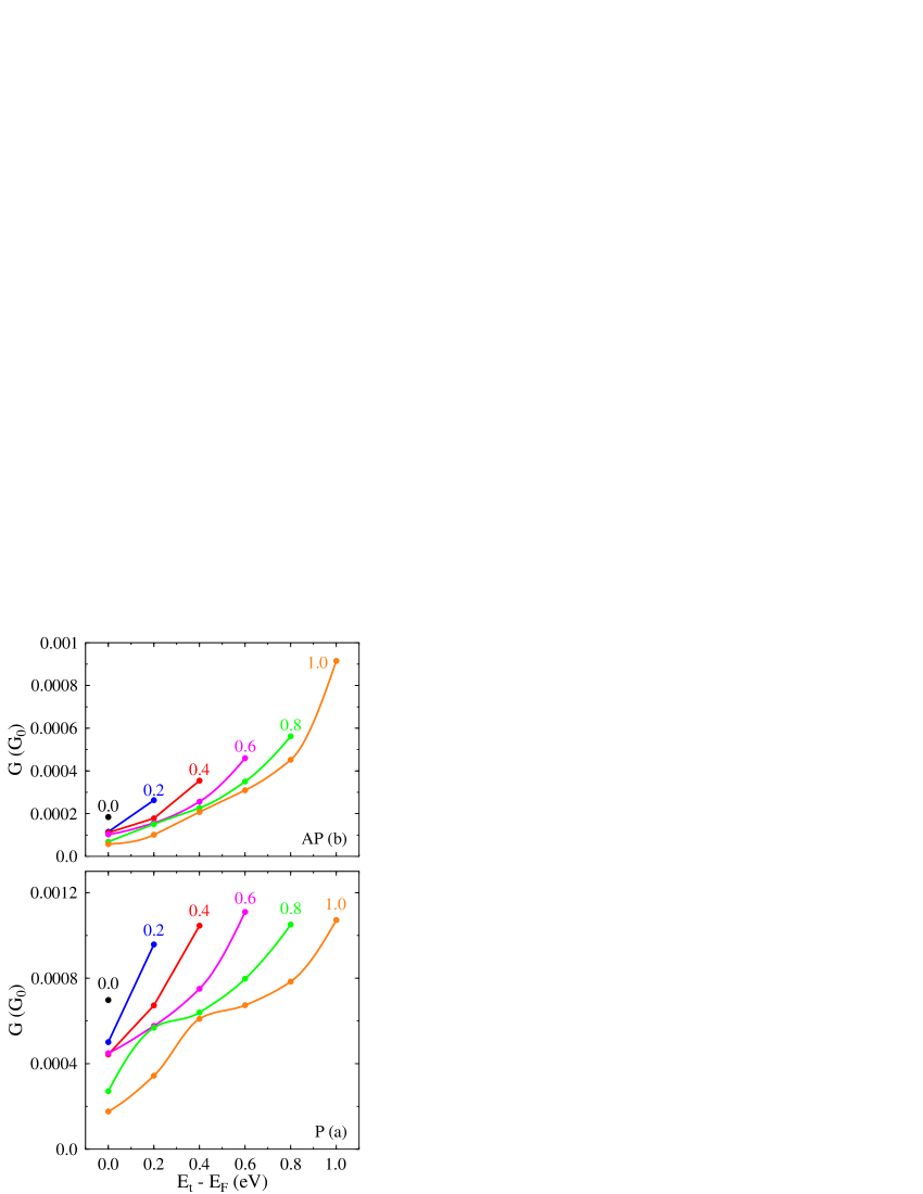
With increasing bias, the conductances for tunneling at decrease. Since ballistic tunneling is a phase coherent process, shifting of the electronic states of one electrodes relative to those of the other by the bias, might reduce the phase coherence. Or the spin-dependent DOS in the relevant region of the 2BZ decreases with energy. We checked the spectral density carefully but found no significant feature that would corroborate unequivocally the latter explanation.
The conductances increase with tunnel energy (cf. the data for to bias). This fact might be explained by the electronic structure of the leads or by a reduction of the effective barrier width and height (cf. Figs. 3 and 5). Indeed, the radius of the ring-like structure in the 2BZ which contributes most to the conductance (cf. Fig. 6) gets larger with tunnel energy, hence increasing the contributing area. This is consistent with the focusing effect mentioned earlier. The AP conductances in particular can be represented reasonably well by parabolae.
A further interesting feature is the increase for biases of , , and eV that occurs for P alignment at tunnel energies around , , and eV, respectively (Fig. 7a). Inspection of the transmissions and of the spectral density at produced no significant feature that would explain this behavior (This is corroborated by findings of LeClair et al., Ref. LeClair et al., 2002). The feature occurs also for AP alignment (Fig. 7b) but not as pronounced as for the P case.
The increase with bias compensates the decrease for , as is shown for the averaged conductances in Fig. 8a.
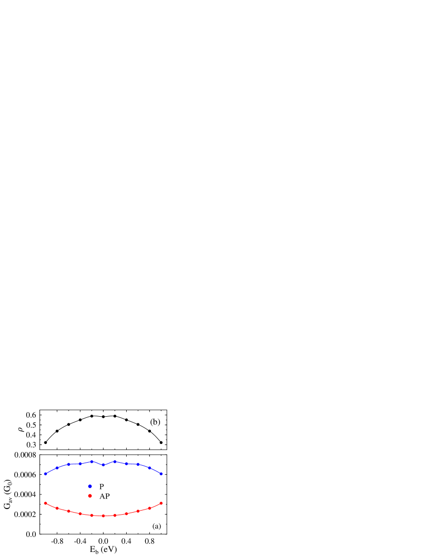
Whereas decreases slightly (with a small minimum at zero bias), increases with . Therefore, the resulting TMR [eq. (12)] drops with bias, too. However, the decrease which is about at is much less than that observed for oxide barriers. In the latter case, the TMR drops by to at . Yuasa et al. (2002) Being due to the details of the electronic structure in the Co leads, one could term the drop in Fig. 8b as ‘DOS effect’, rather than as zero-bias anomaly.
Since inelastic processes (scattering at magnons, spin excitations) are not included in our theory, one can conclude that the ZBA found in tunnel junctions with oxide barriers can be attributed to defect scattering in the oxide barrier. This finding is consistent with the fact that the ZBA decreases with the improvement of the preparation techniques for ferromagnet-oxide interfaces (see Ref. Ding et al., 2003 and references therein).
In a previous investigation, Ding et al. (2003) we used the superposition approach (II.2.3) for the tunnel barrier. There, both the averaged conductances and the TMR were almost constant for biases up to . Comparing with the present results that were obtained within the image-potential approach (II.2.2), one has to keep in mind that details of the calculations differ (e. g., the mesh). However, these have only minor influence. The most striking difference is the shape of the tunnel barrier which is varied in two aspects. First, the JJJ barrier used in Ref. Ding et al., 2003 is rather smooth with respect to the interpolating Lorentzian chosen here. Generally speaking, the latter produces a larger reflection. Second, the shape in the central part of the barrier differs. In particular for large lead separations, the barrier height becomes important (cf. Figs. 3 and 5). Further, the linear bias potential which is missing in the superposition approach is expected to have a non-negligible effect. Therefore, details of the barrier are expected to have significant influence on the tunnel magneto-resistance.
IV Concluding remarks
Tunnel calculations provide a rather indirect test of the proposed barrier shapes. A more direct one would be to compare theoretical energy positions and linewidths of so-called field-emission resonances Gadzuk (1993) with experimental ones. These electronic states can be viewed as surface states that are trapped between the bulk (in the presence of a bulk-band gap) and the tunnel barrier between sample and an STM tip. The field-emission resonances show up as sharp maxima in the differential conductance and depend—like the shape of the tunnel barrier—on both bias voltage and tip-sample separation.
As a possible extension of the present work, one could think of a treatment of tunnel junctions with ‘filled’ spacers (instead of vacuum), in particular with oxide barriers. Further, work is in progress to describe the tunneling with bias voltage fully on an ab-initio level.
Acknowledgements.
We would like to thank Hai Feng Ding, Arthur Ernst, Ingrid Mertig, Silke Roether, Wulf Wulfhekel, and Peter Zahn for stimulating discussions.References
- Maekawa and Shinjo (2002) S. Maekawa and T. Shinjo, eds., Spin Dependent Transport in Magnetic Nanostructures (Taylor & Francis, London, 2002).
- Slonczewski (1989) J. C. Slonczewski, Phys. Rev. B 39, 6995 (1989).
- Jullière (1975) M. Jullière, Phys. Lett. A 54, 225 (1975).
- Gross and Dreizler (1995) E. K. U. Gross and R. M. Dreizler, eds., Density Functional Theory, vol. 337 of NATO ASI Series B Physics (Plenum Press, New York, 1995).
- Reiss (1990) H. R. Reiss, Phys. Rev. A 42, 1476 (1990).
- Lang (1992) N. D. Lang, Phys. Rev. B 45, 13 599 (1992).
- Wulfhekel et al. (2002) W. Wulfhekel, H. F. Ding, and J. Kirschner, J. Magn. Magn. Mater. 242–245, 47 (2002).
- Ding et al. (2003) H. F. Ding, W. Wulfhekel, J. Henk, P. Bruno, and J. Kirschner, Phys. Rev. Lett. 90, 116603 (2003).
- LeClair et al. (2002) P. LeClair, J. T. Kohlhepp, C. H. van de Vin, H. Wieldraaijer, H. J. M. Swagten, W. J. M. de Jonge, A. H. Davis, J. M. MacLaren, J. S. Moodera, and R. Jansen, Phys. Rev. Lett. 88, 107201 (2002).
- Wunnicke et al. (2002) O. Wunnicke, N. Papanikolaou, R. Zeller, P. H. Dederichs, V. Drchal, and J. Kudrnovský, Phys. Rev. B 65, 064425 (2002).
- Wang et al. (2003) K. Wang, P. M. Levy, S. Zhang, and L. Szunyogh, Phil. Mag. 83, 1255 (2003).
- McRae and Kane (1981) E. G. McRae and M. L. Kane, Surf. Sci. 108, 435 (1981).
- Chulkov et al. (1999) E. V. Chulkov, V. M. Silkin, and P. M. Echenique, Surf. Sci. 437, 330 (1999).
- Graß et al. (1993) M. Graß, J. Braun, G. Borstel, R. Schneider, H. Dürr, T. Fauster, and V. Dose, J. Phys.: Condens. Matt. 5, 599 (1993).
- Mac Coll (1939) L. A. Mac Coll, Phys. Rev. 56, 699 (1939).
- (16) We use atomic Hartree units, , .
- Cutler and Gibbons (1958) P. H. Cutler and J. J. Gibbons, Phys. Rev. 111, 394 (1958).
- Jones et al. (1984) R. O. Jones, P. J. Jennings, and O. Jepsen, Phys. Rev. B 29, 6474 (1984).
- Rundgren and Malmström (1977) J. Rundgren and G. Malmström, J. Phys. C: Sol. State Phys. 10, 4671 (1977).
- Malmström and Rundgren (1980) G. Malmström and J. Rundgren, Comp. Phys. Commun. 19, 263 (1980).
- Tamura and Feder (1990) E. Tamura and R. Feder, Z. Phys. B81, 425 (1990).
- Tamura and Feder (1983) E. Tamura and R. Feder, Vac. 33, 864 (1983).
- Lent and Kirkner (1990) C. S. Lent and D. J. Kirkner, J. Appl. Phys. 67, 6353 (1990).
- Joly (1992) Y. Joly, Phys. Rev. Lett. 68, 950 (1992).
- Henk et al. (1993) J. Henk, W. Schattke, H. Carstensen, R. Manzke, and M. Skibowski, Phys. Rev. B 47, 2251 (1993).
- Lorenz et al. (1997) S. Lorenz, C. Solterbeck, W. Schattke, J. Burmeister, and W. Hackbusch, Phys. Rev. B 55, R13 432 (1997).
- Abramowitz and Stegun (1970) M. Abramowitz and I. A. Stegun, eds., Handbook of Mathematical Functions (Dover Publications, New York, 1970).
- Limot et al. (2003) L. Limot, T. Maroutian, P. Johansson, and R. Berndt (2003), cond-mat/0301568.
- MacLaren et al. (1999) J. M. MacLaren, X.-G. Zhang, W. H. Butler, and X. Wang, Phys. Rev. B 59, 5470 (1999).
- Büttiker (1986) M. Büttiker, Phys. Rev. Lett. 57, 1761 (1986).
- Henk (2001a) J. Henk, in Handbook of Thin Film Materials, edited by H. S. Nalwa (Academic Press, San Diego, 2001a), vol. 2, chap. 10, p. 479.
- Henk (2001b) J. Henk, Phys. Rev. B 64, 035412 (2001b).
- Math et al. (2001) C. Math, J. Braun, and M. Donath, Surf. Sci. 482–485, 556 (2001).
- Braun and Donath (2002) J. Braun and M. Donath, Europhys. Lett. 59, 592 (2002).
- Okuno et al. (2002) S. N. Okuno, T. Kishi, and K. Tanaka, Phys. Rev. Lett. 88, 066803 (2002).
- Jepsen and Marcus (1971) D. W. Jepsen and P. M. Marcus, in Computational Methods in Band Theory, edited by P. M. Marcus, J. F. Janak, and A. R. Williams (Plenum Press, New York, 1971), p. 416.
- Weinberger (1990) P. Weinberger, Electron Scattering Theory of Ordered and Disordered Matter (Clarendon Press, Oxford, 1990).
- Slater (1937) J. C. Slater, Phys. Rev. 51, 840 (1937).
- Heine (1963) V. Heine, Proc. Phys. Soc. 81, 300 (1963).
- Davis and MacLaren (2000) A. H. Davis and J. M. MacLaren, J. Appl. Phys. 87, 5224 (2000).
- Yuasa et al. (2002) S. Yuasa, T. Nagahama, and Y. Suzuki, Sci. 297, 234 (2002).
- Gadzuk (1993) J. W. Gadzuk, Phys. Rev. B 47, 12 832 (1993).