High temperature gate control of quantum well spin memory
Abstract
Time-resolved optical measurements in (110)-oriented GaAs/AlGaAs quantum wells show a ten-fold increase of the spin-relaxation rate as a function of applied electric field from 20 to 80 kV cm-1 at 170 K and indicate a similar variation at 300 K, in agreement with calculations based on the Rashba effect. Spin relaxation is almost field-independent below 20 kV cm-1 reflecting quantum well interface asymmetry. The results indicate the achievability of voltage-gateable spin-memory time longer than 3 ns simultaneously with high electron mobility.
pacs:
72.25.Fe, 72.25.Rb, 78.47.+pThe longest possible spin memory and an ability to control the orientation or relaxation of non-equilibrium spin populations in semiconductor quantum wells (QWs) via an applied gate voltage will be the key to many spintronic applications. Recent experiments on (110)-oriented III-V QWs have demonstrated a predicted Oh99 (1, 2) dramatic increase of spin memory at room temperature, up to 20 ns in an -type GaAs/AlGaAs QW Ada01 (3), but although various possible approaches exist, gate control has hitherto been more elusive. The dependence of carrier spin relaxation rates on gate-injected electron or hole concentration in QWs has been investigated by optical techniques Sn90 (4, 5). A second approach exploits the electric field dependence of the electron -factor in parabolic potential wells to control spin precession in applied magnetic field Sal02 (6). Similarly gated ferromagnetism in transition-metal-doped III-V’s Oh00 (7) may allow control of spin orientation without an applied magnetic field. A third proposal is to manipulate the conduction band spin-splitting by an applied electric field through the Rashba effect Ra60 (8). This permits gate control of the exponential spin relaxation at high temperatures where electrons experience strong scattering, the so called collision-dominated regime, Lau02 (9) or even coherent spin reorientation under collision-free conditions at very low temperatures DD90 (10). For the collision-dominated case this last approach has the strong advantage of applicability at room temperature.
In this paper we report a time-resolved optical investigation of electron spin relaxation at high-temperatures in undoped (110)-oriented GaAs/AlGaAs QWs. We confirm the existence of a 100-fold increase of spin memory compared to (001)-oriented QWs at 300 K Oh99 (1) but we now demonstrate a ten-fold variation of the spin relaxation rate with the application of a modest electric field. This is in accord with theoretical expectations Lau02 (9) for the Rashba effect and strongly indicates the mechanism which currently limits the spin memory in (110)-oriented samples in zero field.
The spin relaxation in our experiments can be interpreted on the basis of the D’yakonov, Perel’ and Kachorovskii (DPK) DK86 (2, 11) mechanism of spin relaxation, as refined in a non-perturbative approach Lau02 (9, 12, 13), which dominates zero-field spin dynamics in GaAs/AlGaAs QW systems Fl02 (13, 14, 15, 16). In this model, spin reorientation is driven by precession of the individual electron spin vectors induced by the effective magnetic field represented by the conduction band spin splitting, which results from spin-orbit coupling and lack of inversion symmetry. The corresponding Larmor precession vector varies in magnitude and direction according to the electron’s wavevector so that scattering results in a randomly fluctuating precession vector DK86 (2, 11, 17). In the collision-dominated regime, with the average precession frequency and the momentum scattering time of an electron, spin relaxation is inhibited by scattering and has rate DK86 (2, 11, 13)
| (1) |
The first factor in this expression is determined by the vector , which, in a QW, has three contributions, , and Fl02 (13). The natural interface asymmetry component does not occur in GaAs/AlGaAs QWs and is not considered further here. The most interesting for gating spin relaxation is , the Rashba or structural inversion asymmetry (SIA) term. It may arise from some built-in asymmetry of the structure or be induced by an externally applied odd parity perturbation such as an electric field. For field along the growth axis () it has the form () Ra60 (8, 13) and so is oriented in the QW plane for all in-plane . This induces precession of the electron spin away from the -axis and therefore contributes a term to DPK spin relaxation along the axis, which can be varied with applied electric field Lau02 (9). However except in (110)-oriented QWs the effect will be small because , which is due to bulk inversion asymmetry (BIA) of the zinc blende structure and is only weakly field-dependant, is either wholly or partially in the QW plane and so swamps Lau02 (9, 10, 17). For the special case of (110)-oriented QWs, illustrated in Fig. 1,
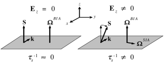
lies approximately along the growth axis for all , causing only weak spin relaxation along the growth axis and thereby leading to greatly enhanced spin memory, as predicted by D’yakonov and Kachorovskii DK86 (2) and confirmed experimentally by Ohno et al. Oh99 (1). Spin relaxation along the growth axis therefore becomes more sensitive to and should be significantly changed by the application of an external electric field Lau02 (9), an important possibility, which we investigate here.
Equation (1) also shows that the spin relaxation rate scales with in a way analogous to motional narrowing. For undoped QWs, is closely related to the momentum relaxation time which determines the electron mobility DK86 (2, 11, 13). This means that long spin memory and high mobility are, in general, mutually exclusive in low-doped -type QWs but may be simultaneously achievable in the special case of (110)-oriented QWs.
Samples from three different wafers have been studied each grown on a semi-insulating (SI) GaAs substrate and each containing twenty 7.5 nm QWs separated by 12 nm barriers with aluminium fraction 0.4. Two wafers consisted only of undoped layers on (001)- and (110)-oriented substrates respectively. The third wafer was a structure on a (110)-oriented substrate with the undoped QWs grown between two 0.1 m undoped buffer layers of AlGaAs and with layers of 2 cm-3 doped GaAs and of 1.2 cm-3 doped AlGaAs respectively below and above. The orientation of the (110)-oriented substrates was accurate to . Measurements were carried out at 300 K on all three wafers as grown and the wafer was also processed into 400 m mesa devices (Fig. 2a) and used for measurements in variable electric field at 170 K. Although the sequence of layers in the samples does not have inversion symmetry, for flat-band conditions the QWs and barriers possess local inversion symmetry where the confined electron wavefunctions have significant density. The doped layers of the structure result in a built-in electric field of about 25 kV cm-1. Figure 2b shows the photoluminescence (PL) spectrum of one of the mesa structures for zero applied bias at 170 K. The width, at 10 K, of the excitonic recombination line was 6.5 meV in each of our (110)-oriented wafers and 1.8 meV in our (001)-oriented wafer. Since we expect similar fluctuations in QW width for the two sets of multi-quantum wells (MQWs), this suggests that the interfaces of the (110)-oriented QWs are less perfect than for (001) growth and could be further improved by variation of growth conditions.
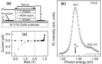
Electron spin evolution was obtained from the change of intensity and polarisation rotation of optical probe pulses reflected at near normal incidence from the sample surface along the growth axis, at a variable delay following excitation by 10 times more intense, nearly collinear circularly polarised pump pulses DD90 (10, 14, 16). The pulses were of 2 ps duration from a mode-locked Ti-sapphire laser tuned to the peak of the first electron-heavy-hole PL transition (Fig. 2b) giving excitation density 109 cm-2. Figure 2c shows the - characteristics of the device in the dark and illuminated with experimental laser intensity, 350 W. Such low powers are necessary to avoid screening of the electric field in the MQW region. Since this incident intensity could generate a photocurrent up to 30 A, the magnitude of the negative bias current shows that in fact a very small fraction, 2, of the photo-carriers is swept out by the bias but even this may be exaggerated because the rapid increase of current below 1.5 volts indicates avalanche multiplication. The absorbed pump photons thus generate ‘cold’ excitons which dissociate into free carriers on a sub-picosecond timescale with spins polarised along the growth axis and which remain confined in the QWs. The hole spins rapidly relax whereas the electron spin-relaxation is much slower Br98 (14, 16). On a timescale longer than 1 ps, gives a measure of the population of photoexcited carriers and a measure of the -component of electron spin so that their ratio gives the pure longitudinal spin dynamics of the electrons Br98 (14, 16).
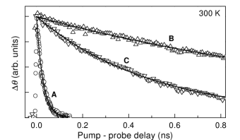
Figure 3 shows the observed signals for the three as-grown wafers at 300 K. There is a dramatic difference between the decay for the (001)-oriented wafer (A) and the undoped (110)-oriented wafer (B), which essentially reproduces the findings of Ohno et al. Oh99 (1). However the decay for the (110)-oriented wafer (C), where there is a built-in electric field of about 25 kV cm-1 (at 300 K), is significantly faster than for the undoped (110)-oriented wafer (B). Measurements were made at various pump intensities to allow extrapolation to zero power and when the decay of the signal is also included in each case the spin relaxation times are found to be ps, ns and ns for A, B and C wafers respectively. These figures are consistent with our theoretical predictions Lau02 (9) if we assume electron mobilities 0.4 m2 V-1s-1, 0.3 m2 V-1s-1 and 0.43 m2 V-1s-1 respectively. Although we do not have direct mobility measurements, these are reasonable room temperature values for such samples where optical phonon scattering and interface roughness are likely to be dominant Br98 (14). Figure 3 therefore gives a strong indication that there is a significant variation of spin relaxation rate with electric field at 300 K as predicted theoretically Lau02 (9).
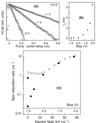
Measurements on the mesa devices at different bias voltages at 170 K (Fig. 4a) support this conclusion (measurements at 300 K for the same range of voltages were prevented by excessive current in reverse bias leading to destruction of the device). The signals show single-exponential decay and there is a strong variation of decay rate with voltage. The signals also decay exponentially and Fig. 4b shows the extracted decay times () as a function of bias. For large negative bias increases significantly reflecting the reduced electron-hole overlap at high electric fields and showing that recombination is predominantly radiative Pol85 (18).
Figure 4c shows the spin relaxation rate vs bias voltage and vs the corresponding electric field at the QWs obtained using the layer thicknesses in the structure and the band gap of GaAs at 170 K. Up to 20 kV cm-1 the spin relaxation rate is almost constant but then increases by about a factor of 10 by 80 kV cm-1. The solid dots are results of our non-perturbative calculations Lau02 (9, 12, 13) based on the DPK mechanism for a symmetrical (110)-oriented QW. The calculations assumed electron mobility of 0.6 m2 V-1s-1, which is consistent with the assumed 300 K value in the wafer, 0.43 m2 V-1s-1, for mobility limited by optical phonon scattering in this temperature range. The variation for electric fields greater than 20 kV cm-1 (Fig. 4c) is very well fitted by the theory but at lower fields there is clearly a contribution to the spin relaxation not included in the calculations which predict a rate almost 100 times lower than we have observed at zero field.
The measured decay rates in this region were found to increase linearly with pump power, consistent with a small influence of the Bir, Aronov and Pikus (BAP) relaxation mechanism BAP76 (19) due to exchange interaction with the photo-excited holes as also found by Adachi et al. Ada01 (3). This does not, however, explain the observed discrepancy with theory since extrapolation to zero power would only make a reduction of about 10. Nor can it be explained in terms of the BAP mechanism with electrically injected holes; even for flat band conditions in forward bias, where the injected hole concentration would be greatest, the calculated concentration is at least two orders of magnitude too low to explain the additional spin relaxation BAP76 (19). Another possible cause of the additional spin relaxation is random built-in asymmetry in the QWs, which would give a field-independent SIA contribution. Such asymmetry could result from alloy fluctuations or from differences of top and bottom interface morphology for the GaAs/AlGaAs QWs and for a given would generate an component varying randomly in magnitude and orientation from point to point on a QW with associated non-zero mean square entering Eq. (1). To gauge this possibility, we have repeated our calculation in zero field for a QW with one perfect interface and the other containing a two-monolayer compositional gradient. The relaxation rate is 30 times greater than for a perfectly symmetrical QW (solid square in Fig. 4c). Even this small perturbation of the symmetry produces a change approaching our discrepancy between theory and experiment supporting the idea that the spin memory is actually limited by the sample perfection which, as indicated by the width of luminescence lines may be somewhat inferior to that in (001)-oriented samples. At sufficiently high reverse bias the increase of the relaxation rate due to the applied field becomes dominant over this random built-in asymmetry.
In conclusion, we have demonstrated that the enhanced high-temperature electron spin memory in (110)-oriented QWs may be varied by at least a factor 10 by application of modest gate bias voltages. The variation is consistent with the Rashba effect and the DPK spin-relaxation mechanism. On the basis of this mechanism, the measurements for low electric fields indicate that a further significant enhancement of spin memory may be achieved by modification of the growth techniques to optimise the interface morphology. This may be expected to give at 300 K spin memory longer than 10 ns Lau02 (9, 3) and straightforward voltage bias control simultaneously with high electron mobility. This combination of properties will facilitate a variety of spintronic devices.
Acknowledgements.
We wish to thank Professor E. L. Ivchenko, Mr M. M. Glazov and Dr. K. V. Kavokin for many illuminating discussions. This work was supported by EPSRC and DARPA/ARO.References
- (1) Y. Ohno et al., Phys. Rev. Lett. 83, 4196 (1999).
- (2) M. I. D’yakonov and V. Yu. Kachorovskii, Sov. Phys. Semicond. 20, 110 (1986).
- (3) T. Adachi et al., Physica E 10, 36 (2001).
- (4) M. J. Snelling et al., J. Luminescence 45, 208 (1990).
- (5) J. S. Sandhu et al., Phys. Rev. Lett. 86, 2150 (2001).
- (6) G. Salis et al., Nature (London) 414, 619 (2002); for review see: D. D. Awschalom, D. Loss and N. Samarth, eds., Semiconductor Spintronics and Quantum Computation (Springer, 2002), chap. 5: Optical Manipulation of Spin Coherence in Semiconductors by D. D. Awschalom and N. Samarth.
- (7) H. Ohno et al., Nature (London) 408, 944 (2000).
- (8) E. I. Rashba, Sov. Phys. Solid State 2, 1109 (1960); Y. A. Bychkov and E. I. Rashba, J. Phys. C 17, 6039 (1984).
- (9) W. H. Lau and M. E. Flatté, J. Appl. Phys. 91, 8682 (2002).
- (10) S. Datta and B. Das, Appl. Phys. Lett. 56, 665 (1990); M. A. Brand et al., Phys. Rev. Lett., 89, 236601 (2002).
- (11) M. I. D’yakonov and V. I. Perel’, Sov. Phys. JETP 33, 1053 (1971).
- (12) W. H. Lau, J. T. Olesberg and M. E. Flatté, Phys. Rev. B 64, 161301 (2001).
- (13) for review see: D. D. Awschalom, D. Loss and N. Samarth, eds., Semiconductor Spintronics and Quantum Computation (Springer, 2002), chap. 4: Spin Dynamics in Semiconductors by M. E. Flatté, J. M. Byers and W. H. Lau.
- (14) R. S. Britton et al., Appl. Phys. Lett. 73, 2140 (1998).
- (15) R. Terauchi et al., Jpn. J. Appl. Phys. 38, 2549 (1999).
- (16) A. Malinowski et al., Phys. Rev. B 62, 13034 (2001); R. T. Harley, O. Z. Karimov and M. Henini, J. Phys. D, in press.
- (17) B. Jusserand et al., Phys. Rev. B 51, 4707 (1995).
- (18) H. -J. Polland et al., Phys. Rev. Lett. 55, 2610 (1985).
- (19) G. L. Bir, A. G. Aronov and G. E. Pikus, Sov. Phys. JETP 42, 705 (1976); G. Fishman and G. Lampel, Phys. Rev. B 16, 820 (1977); for review see: F. Meier and B. P. Zakharchenya, eds., Optical Orientation (North-Holland, 1984).