Normal-superconducting transition induced by high current densities in YBa2Cu3O7-δ melt-textured samples and thin films: Similarities and differences.
Abstract
Current-voltage characteristics of top seeded melt-textured YBa2Cu3O7-δ are presented. The samples were cut out of centimetric monoliths. Films characteristics were also measured on microbridges patterned on thin films grown by dc sputtering. For both types of samples, a quasi-discontinuity or quenching was observed for a current density several times the critical current density . Though films and bulks much differ in their magnitude of both and , a proposal is made as to a common intrinsic origin of the quenching phenomenon. The unique temperature dependence observed for the ratio , as well as the explanation of the pre-quenching regime in terms of a single dissipation model lend support to our proposal.
pacs:
74.25.Fy, 74.25.Sv, 74.81.Bd, 74.72.BkI Introduction
Measurement of Current-Voltage Characteristics (CVCs) of high temperature superconductors provides important information on critical current and dissipation mechanism, enhancing our knowledge about the vortex dynamics of these materials and about their practical applicability.Blatter et al. (1994); Tinkham (1996) The mentioned properties are very sensitive to microstructure (presence of grain boundaries, microcracks, twin-planes or different kinds of bulk and surface defects), as well as to external conditions (temperature and magnetic field). As a consequence, CVCs are expected to highly depend on these features as well. In the low dissipative regime, the CVCs have been widely studied for polycrystalline bulks, melt textured samples, films and single crystals. Several theories have been given to explain the observed CVCs: flux flow, flux creep, collective flux pinning, vortex glass transition…Blatter et al. (1994); Tinkham (1996)
The highly dissipative regime at high current densities has received attention recently and results are available for films.Samoilov et al. (1995); Klein et al. (1985); Lefloch et al. (1999); Currás et al. (2001); Xiao and Ziemann (1996); Xiao et al. (1998a); Doettinger et al. (1994, 1995); Antognazza et al. (1999); Decroux et al. (2000); Chiaverini et al. ; Xiao et al. (1998b, 1999); Reymond et al. (2002) The common observation is that, below , a transition to a highly dissipative regime takes place abruptly at a certain current density several times the critical current density . In this high dissipative regime, the effective resistivity almost agrees with the normal resistivity extrapolated to the sample temperature, . Here, is the electric field parallel to the applied current density . This quasi-discontinuity in the CVCs, sometimes called quench, has been observed for films of low critical temperature Samoilov et al. (1995); Klein et al. (1985); Lefloch et al. (1999) and high critical temperature (YBa2Cu3O7-δ Currás et al. (2001); Xiao and Ziemann (1996); Xiao et al. (1998a); Doettinger et al. (1994, 1995); Antognazza et al. (1999); Decroux et al. (2000) and Bi2Sr2CaCu2O8+δ Chiaverini et al. ; Xiao et al. (1998b, 1999); Reymond et al. (2002)) superconductors. The quench is usually explained by the Larkin-Ovchinnikov theory, Larkin and Ovchinnikov (1976) in terms of a high acceleration of vortices when they reach a certain critical velocity, and by its modified version by Bezuglyj and Shklovskij Bezuglyj and Shklovskij (1992) including heating effects as a refinement to the LO theory. These theories have dropped the more classical explanation based in the existence of a thermal bistability in these materials Skocpol et al. (1974); Gurevich and Mints (1987); Skokov and Koverda (1993), thus only needing heating effects to justify the existence of a quasi-discontinuity in the CVCs. There are also other authors which explain the quench using arguments similar to the one dimensional phase-slip centers theory.Jelila et al. (1998); Maneval et al. (2001); Reymond et al. (2002)
Electrical transport measurements up to high current densities, inducing the transition to the normal state, have been also carried out in melt texturedPorcar et al. (1998); Tixador et al. (2000); Tournier et al. (2000); Yang et al. (1999); Morita et al. (1999, 2000) (and melt castHerrmann et al. (1997); Elschner et al. (1999)) samples, only at 77 K or some other particular temperatureTixador et al. (1999). Bulk superconductors are specially attractive because of their great potential for applications at high transport currents. Again, a similar abrupt increase of voltage has been observed in the CVCs of these materials. However, in this case, the usual explanations do not come from intrinsic vortex dynamics, but from thermal processes (thermal runaway Elschner et al. (1999); Tournier et al. (2000) or changes in the dissipation regime of the samplesYang et al. (1999)).
As a support for such divergent approaches to monoliths and films, phenomenological, structural and morphological reason can be invoked. The more obvious difference between the two kinds of samples is their critical current density, . Melt-textured samples have a around – A/cm2, for a typical section between 0.5 and 15 mm2, while of films exceeds A/cm2, for samples of typical thickness of 0.1-0.5 m, and a more variable width, between 10 m and 1 mm. Usually, this difference in the values is attributed to structural causes: presence of more and stronger pinning centers, lesser effect of possible grain boundaries or microcracks…, or also to current concentration on the outer surface of samplesLazard et al. (2002). No less meaningful differences exist in their thermal environment. The levity of films together with a close lattice matching with the substrate favor a good refrigeration and a fast reaching of the steady state. Bulk material, in turn, is massive and quite inevitably inhomogeneous, both features leading to a poor refrigeration and hot spot development.
Despite these marked differences, the similarity of the overall quenching phenomenon seen in the CVCs for films and bulk samples demands a more exhaustive measurement of the latter, and closer comparative study between them. In fact, though there are contributions that study both type of samples at the onset of dissipation at different temperatures and magnetic fieldsGao et al. (1991); Yang et al. (1992); Solovjov et al. (1994); Elschner et al. (1994); Hettinger et al. (1989); Gupta et al. (1993); Cao et al. (1997); Wang et al. (2000), we are not aware of similar studies for melt-textured samples extending to high current densities, and, in particular, the quenching effect. This paper is devoted to a systematic comparison of dissipation and particularly the quench phenomenon in both melt-textured (bulk) and thin films. The aim is to look closely into the phenomenological behavior of charge transfer at high density in both systems, in order to infer a possible shared origin of the quenching. This voltage jump is also very interesting for applications of both melt-textured samples and films like fault current limiters, as it means a fast change in the resistance of the device for currents above a critical value.
Systematic measurement of CVCs on melt-textured samples of YBa2Cu3O7-δ (YBCO) have been carried out at various temperatures. For spurious heating to keep moderately low, a near temperature range has been scanned, where critical current values are lower. At the same time, refrigeration conditions were optimized by using a pressurized cryostat so that samples were always submerged in liquid nitrogen at any temperature. A comparison with CVCs measured in YBCO films at different temperatures was carried out, studying the low dissipative regime before the quasi-discontinuity, as well as the occurrence of the quasi-discontinuity itself.
II Experimental details
II.1 Melt-textured samples
Single domain bulk samples of YBa2Cu3O7-δ plus 30 molar % Y2BaCu and 0.1 wt. % Pt were prepared by top seeded melt growth (TSMG)Cardwell (1998); Lo et al. (1996). Commercial powders of YBa2Cu3O7-δ, Y2BaCuO5 and Pt were mixed in the above proportions, and 30 g samples of this mixture were die pressed into 3 cm diameter pellets. These were placed on MgO single crystal substratesEndo et al. (1996) in a box furnace, and heated to 1025 oC to be decomposed peritectically. After a fast decrease of temperature to 990 oC, the samples were slowly cooled to around 960 oC at 0.3-0.4 oC/h. In order to control the growth of YBCO during the cooling and avoid the formation of a granular microstructure, a small seed of Nd-Ba-Cu-O was placed over the samples. After the process, single domain monoliths up to 2 cm in diameter (ab-planes direction) and 0.7 cm in height (c-axis direction) were grown. The microstructure of the samples was studied using optical microscopy and their texture was analyzed by x-ray diffraction. The general characteristics of these melt-textured samples were much the same as those previously obtained following a similar procedure by Cardwell and coworkers.Cardwell (1998); Lo et al. (1996)
Bars with typical dimensions of 0.5 mm2 cross section and 7 mm in length were cut from the monoliths, using a wire saw. We took the crystallographic ab-planes parallel to the longest dimension, so that the current will flow along the ab-planes in the transport measurements. Measurements of the variation of resistivity with temperature for these samples were routinely made.
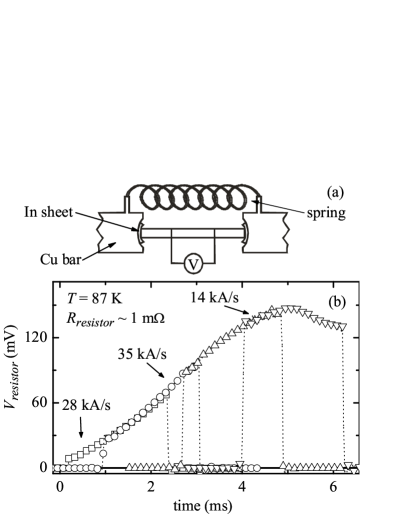
As we have already mentioned, the critical current density in the ab-planes direction for melt-textured samples is of the order of A/cm2, which means current of hundreds of Amperes for our samples. Moreover, we are interested in measuring the – curve for currents well above . The experimental setup for transport measurements must take these features into account, and be designed to minimize the unavoidable heating effects. To reach this aim, the electrical contacts with the sample are one of the main points. The samples were painted in their ends with silver paste and then annealed briefly at 900 oC, to favor the diffusivity of the silver into themNeal et al. (1991); Lepropre et al. (1993); Svistunov et al. (1998). Then, they were cooled down to 500 oC and held at this temperature for several hours to finishing the contacts treatment and to ensuring oxygenationEkin (1993). We obtain a typical contact resistance of 100 at the working range of temperature. The sample is connected with the rest of the circuit through copper bars which are pressed to the sample by springs. An Indium sheet was placed in between (avoiding the Indium to touch the sampleEkin (1993)) to reduce the contact resistance.Maehata et al. (1999) In this way, possible damages by mechanical stress during the transport measurement are also prevented. A scheme of this experimental arrangement is shown in Fig. 1(a).
The second factor to minimize heating effects is refrigeration. All our measurements were made with the sample, plus a reference resistor in-series with it, placed in a hermetic cavity filled up with liquid nitrogen. A valve lets control the pressure of the nitrogen vapor in the cavity, and therefore control the temperature of the liquid nitrogen bath. Furthermore, there is a nitrogen gas reservoir connected with the cavity for a better control and stabilization of pressure.Díaz et al. (1997); Currás et al. (2001)
Finally, we minimized the time that the current goes through the sample. We worked with 1–3 ms long ramp shaped current pulses, as in certain cases longer pulses may burn out the samples. For current application, we use a HP6681A power supply, which has fixed raising ramps to a stable current of approximately 20 ms. Therefore, we used high speed solid-state relays in order to cut the current and isolated 1–3 ms long ramped pulses. Depending on the range of current and the resistance of the sample, the raising rate of the supply varies between 5 and 35 kA/s. As we have limited the total length of the pulse, the total – curve were sometimes obtained as the result of several different pulses. Figure 1(b) shows the shape of some of the current pulses used in this work. During the current pulses, the voltage in the sample and in the reference resistor were recorded with a high speed data acquisition card (DAQ) of National Instruments (PCI-4452) allowing the recording of several voltages simultaneously. From the reference resistor voltage, the current flowing through the circuit at any time was determined. By pressuring the hermetic cavity, we set the sample immersed in liquid nitrogen at the critical temperature (around 90 K). – curves were measured for temperatures from this value down to temperatures where a significant part of the curve is accesible within the limitations of our power supply.
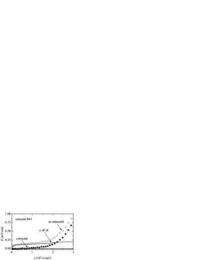
After measuring the – curves, the inductive component of voltage was subtracted: Apart from the self-inductance, there is an inductive component due to the loop that each element forms with the potential wires.Porcar et al. (1997) For the reference resistor, this component is noticeable because its own resistance is very small. We deduced its inductance from the deviation of the – curve from the ohmic behavior when a high resistive element is placed instead of the sample. For the sample, well below , we expect zero resistance for very low current values, so that all the observed voltage should be inductive. Indeed, we found the sample voltage proportional to d/d at low, i.e. subcritical, current. An example of this last correction is shown is Fig. 2. We checked, at different current pulses, the independence of inductance on current raising rate. Inductance is also found temperature independent over our working range of temperature.
II.2 Thin films

| Sample | |||||||
|---|---|---|---|---|---|---|---|
| (mm) | (mm) | (mm) | (K) | (cm) | (A/cm2) | (A/cm2) | |
| A21 | 0.65 | 0.80 | 8.1 | 90.4 | 112 | 0.7 | 3.9 |
| B31 | 0.20 | 0.75 | 7.7 | 89.4 | 78 | 1.5 | 4.0 |
| B44 | 0.35 | 0.65 | 11.2 | 88.9 | 90 | 1.6 | 4.9 |
| C11 | 0.40 | 0.60 | 5.7 | 88.7 | 100 | 1.7 | 8.2 |
| C22 | 0.35 | 0.40 | 7.0 | 88.4 | 43 | 4.2 | 13.4 |
| Sys116 | 1.5 10-4 | 10-2 | 5 10-2 | 90.2 | 102 | 5.0 | 1.3 |
| Sy3 | 1.9 10-4 | 10-2 | 1.0 | 91.0 | 53 | 5.2 | 1.5 |
The two c-axis oriented YBCO thin films used for comparison were grown on (100)SrTiO3 substrates by high pressure dc sputtering. Details about the growth technique and characterization of the films are described elsewhere.Currás et al. (2001) Microbridges of 10 m wide were patterned by chemical wet photolithography and Au contact pads were sputtered on them. After annealing, the typical contact resistance was 100 m. Al wires were solded to these pads using a Kulicke & Soffa 4523 wire bonder. CVCs at different temperatures were measured in four probe configuration, using a different procedure for each of the two films. The film named Sy3 was submerged in a liquid nitrogen container, whose temperature was controlled through its pressure, as explained previously for melt-textured samples. The CVCs were obtained using dc current supplied by a HP6038A power source and cut by a relay: one voltage measurement was taken for every 30 ms constant current pulse, using a HP3457A multimeter.Currás et al. (2001) On the other hand, Sys116 film was set in He atmosphere and its temperature was regulated with an Oxford ITC4 temperature controller. Current was supplied by a Keithley 2400 source, allowing the application of dc current, or stepped ramps of about 1 ms of step length. For the lowest dissipation regime, dc current was used in combination with a HP34420A nanovoltimeter. For higher dissipation, stepped current ramps were measured with a National Instruments PCI6035 DAQ, allowing us to discard inductive effects while acquiring the full CVC in a single measurement of typically 20 ms. An example of these stepped ramps is shown in Fig. 3. The results obtained by the ramps do not significantly differ from those using isolated pulses, as samples seem to reach an almost steady state is less than one millisecond. In fact, voltage was checked to be stable for square pulses around 30 ms long, at currents at least 98% the quenching current, in agreement with previous works Currás et al. (2001). Only for currents very close to the quasi-discontinuity, a progressive increase of the voltage signal was observed, probably due to heating of the sample. In any case, each point in the CVCs is the mean value of voltage data read along a current plateau.
III Results and discussion
III.1 Current Voltage Characteristics
Geometric parameters of our samples and the main results of their corresponding – measurements are summarized in Table 1. is the offset critical temperature, and is the extrapolation of the normal-state resistivity to the working range of temperatures.
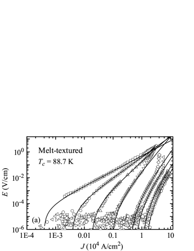
A typical set of CVCs at different temperatures for our melt-textured samples is plotted in Fig. 4, using the standard definitions: and , where is the cross section area and the distance between voltage pads. Fig. 4(b) and (c) are closer views of the low voltage region of Fig. 4(a). Three current regions can be distinguished in the CVCs of Fig. 4. A first region of zero resistance, illustrated in Fig. 4(c). Then, a dissipative region where the voltage grows in a non-linear but smooth way. Finally, there is a sharp change in the voltage up to a nearly normal state behavior. The transition from one of these regions to the next can be characterized by a given value of the current density: is the current density where the dissipation begins, usually obtained by a threshold criterion in the electric field, , while is the current density where the quench in the CVCs occurs. As shown in Fig. 4(a), after the quench, the heat generated in the sample is too high to be evacuated and the CVCs are diverted from the ohmic behavior. For temperatures lower than 3 or 4 degrees below , the rapid increase in the sample resistance is accompanied by a decrease of current (see the last pulse of Fig. 1(b) for an example), as our power supply is not able to respond fast enough to the change of charge. For this reason, at these temperatures, it was not possible to complete the CVC up to the nearly normal state region.
As mentioned in Section II.1, we have used different pulses to measure the CVCs of our melt-textured samples. We have observed a displacement of the quench current to higher values as the initial current of the pulses applied gets higher. This result reveals the importance of thermal effects in the occurrence of the quench. Nevertheless, for temperatures lower than 2 degrees below , we have estimated a variation of in less than 30%, due to this effect, being smaller at lower temperature. This dependence of the CVC results on the pulse features was observed only for currents near the quench, whereas the CVC data for lower currents were well reproduced in different pulses.
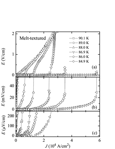
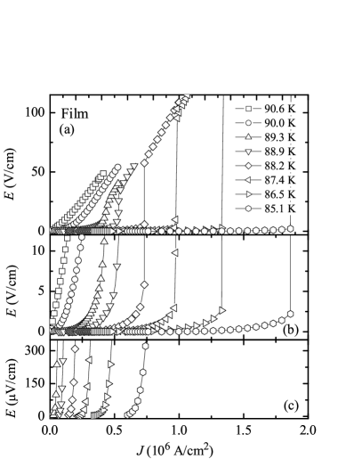
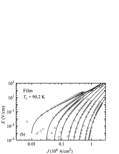
As mentioned in the introduction, similar results have been previously reported for melt textured samples at 77 K. As well, the overall behavior of these CVCs is common to films or melt cast processed samples, but the explanation about the observed abrupt change in the sample resistance at high current densities is variant. While in melt textured and melt cast processed samples the quench is generally attributed to thermal runaway processes,Tournier et al. (2000); Yang et al. (1999); Elschner et al. (1999) there are several authors which explain the abrupt resistance change observed in films as a high flux-flow velocity instability.Doettinger et al. (1994); Xiao and Ziemann (1996); Chiaverini et al. Here, we will closely compare the results obtained for melt-textured samples with similar measurements of CVCs in YBCO thin films at different temperatures. Figure 5 shows the corresponding set of CVCs for the film Sys116. Comparison with Fig. 4 confirms that indeed the general behavior of films matches that of melt-textured samples. We can clearly distinguish three different dissipative regions: zero resistance, non-linear – curve above a certain critical current, and near ohmic behavior after an abrupt voltage discontinuity. On the other hand, this comparison also permit to pointed out a main difference between the CVCs of melt-textured samples and films. As may be checked in Figs. 4 and 5, both and along the whole CVCs are approximately two orders of magnitude higher in films, and this includes and . The abundant results on transport properties for currents near the beginning of dissipation both for melt-textured samplesGao et al. (1991); Yang et al. (1992); Solovjov et al. (1994); Elschner et al. (1994) and filmsHettinger et al. (1989); Gupta et al. (1993); Cao et al. (1997); Wang et al. (2000) had already well established the existence of approximately a factor between values of both kind of samples. From the observation of the CVCs presented in this work, it can be stated that this feature is maintained along the whole CVCs. As a result, the CVCs in both type of samples look scalable in that they differ both in and in a constant factor.
Regarding , Fig. 6 illustrates the comparison between its values for melt-textured samples and films. Despite the different magnitude, shows a dependence on temperature close to , where , for both melt-textured samples and films. In this figure, has been determined by the threshold criterion of 10 V/cm. The estimation of and is a bit more complicated. Looking at the curves of Fig. 5(a) and (b) at low temperature, the quenching point seems easy to be obtained because of the neat jump in voltage. However, the corresponding voltage variation is much less abrupt at higher temperature, close to . Furthermore, bulks show smoother quenching than films (see Fig. 4). In all, a systematic criterion for (, ) determination is needed. By observation of CVCs for several samples and temperatures, we found no specific value of the electric field, power or resistivity, nor a value of their first derivatives, where the quasi-discontinuity systematically occurs. For this reason, a good option is to use a deviation criterion from a background functional form, the latter taken from the agreed-on models for CVCs.
In the next section we study the agreement of several dissipation models to our CVC measurements. Apart from providing us with a functional background for the later extraction of , this correlation will permit us to obtain a detailed comparison between the dissipation mechanism in melt-textured samples and films.
III.2 Dissipation models
The probably most popular model to describe non-linear CVCs of type-II superconductors is the thermally activated flux creep theory Blatter et al. (1994); Tinkham (1996). According to this model, the first observation of non-zero voltage occurs below the depinning critical current , due to the displacement of vortices from a pinning center to other caused by thermal fluctuations. The generalized expression for the voltage at a given current below is:
| (1) |
This generic expression comprises different previously proposed models depending on : for the classical Anderson-Kim flux creep model, valid for conventional type-II superconductors, where the pinning is strong, and the dissipation starts for current near . (depending on the current range, magnetic field and temperature) for collective creep/vortex glass models, which assume the beginning of a collective movement of vortices at in materials with weak pinning, as it is the case of high temperature superconductors. Finally, , for the logarithmic Zeldov model, which is a good approximation of the latter for the high current regime () and leads to the simple expression: , with .
The generalized expression has the inconvenience of having too many free parameters. To begin with, a given value of is only expected to describe a limited region of current. Furthermore, presetting the value of or is needed, because otherwise multiple valid solutions for voltage, , are obtained. Their values should be the coordinates of the transition point from a non-linear - curve (flux-creep regime) to a linear one (flux-flow regime). However, such a transition is not observed in our results, i.e. the CVCs are always non-linear up to the voltage quasi-discontinuity. Some authors Xiao and Ziemann (1997) claim that the quasi-discontinuity in the CVCs may occur at and then and . Even if this is the case, we can not use this information as an input, because is an aside information that we want to extract from the analysis. For these reasons, we used the power law (PL) expression which can be written as:
| (2) |
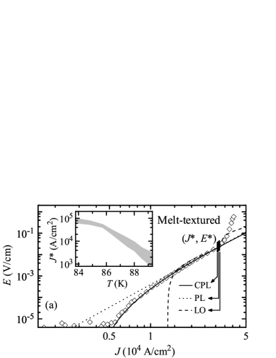
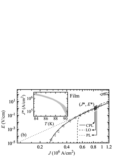
independently on the particular election. Figure 7 shows an example of the fit of the model (dotted lines) to the CVCs for both bulks and films, at a given temperature. The model fits satisfactorily the high current region of the CVCs before the quench, which is the range we are mainly interested in.
Another model suggested in order to explain non-linear - curves, and linked to the nature of the quench, is the non-linear flux-flow theory by Larkin and Ovchinnikov Larkin and Ovchinnikov (1976) (LO). According to this model, the viscosity opposing the movement of vortices in the flux-flow regime varies with their velocity, leading to a non-linear CVC. Moreover, there is a certain critical velocity where viscosity reaches its maximum and then decreases. This causes a rapid acceleration of vortices, which would lead to an abrupt increase of voltage. As already mentioned, several authors state that this could be the correct explanation for the quench observed in filmsDoettinger et al. (1994); Xiao and Ziemann (1996); Chiaverini et al. . Below the predicted quasi-discontinuity, the expression linking and is given by:
| (3) |
where is the resistance in the flux-flow regime. This expression is claimed to fit adequately measurements by other groupsKlein et al. (1985); Doettinger et al. (1994). However, as shown in Fig. 7 (dashed lines), it only fits our measured CVCs very near the transition, both for bulks and films. Moreover, the agreement with our data is not better than the one obtained with the power law.
Finally, we have also inspected another proposed model for non-linear CVCs, which we term critical power law (CPL):
| (4) |
where is the critical current which dissipation begins at. This expression, as happens with the power law given by Eq. (2), may be derived from various physical backgrounds.Prester (1998) In reference to the vortex dynamics, this expression can be obtained modifying the Zeldov expression for thermally activated flux creep model by introducing a threshold to the activation of vortices movement by thermal fluctuations.Antognazza et al. (2002) It can also be deduced in the mean-field approximation for the case of strong pinning and neglecting the effect of thermal fluctuations.Solovjov et al. (1994) On the other hand, the same voltage dependence on current is found in the context of granular materials modelized as an array of Josephson junctions.Prester (1998)
A good agreement has been previously found of the critical power law with CVCs of single crystal and melt-textured samplesSolovjov et al. (1994), and filmsAntognazza et al. (2002), only at limited temperature or current ranges. In this work, we have found a satisfactory fit of this expression to all our CVCs with a value of independent on temperature, leaving two free parameters, and , for each – curve. The improvement in the fit respect to PL or LO expressions, specially for films, is clearly shown in Fig. 7. The agreement with our data is indeed very good over all voltage ranges, as illustrated in Fig. 8. Only for high temperatures, close to , the fit is not good at low current. These CVCs feature a thermally activated flux-flow regime (TAFF) which indicates that we are above the melting temperature,Blatter et al. (1994) and, hence, neither Eq. (1) nor Eq. (4) are expected to hold.
Note that the good agreement of the critical power law with CVCs measured in absence of an external magnetic field should not be surprising: Flux creep theory in materials with weak pinning () states that, even at very low current, thermal fluctuations can cause displacements of vortices from their pinning centers, thus generating a voltage. However, this is the case only in experiments in which vortices are previously created by an external magnetic field above . When no external field is applied, as in our data, the sample will stay in the Meissner state up to currents producing a self-field higher than . For lower currents, no vortices are still present and there is no dissipation. Later, for higher currents, vortices start to be created and may begin to creep. As a result, a threshold for the beginning of dissipation, as the CPL expression features, must be necessary to explain the CVCs.
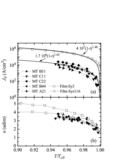
In order to compare the results for melt-textured samples and films, we have plotted in Fig. 9 the values of the parameters obtained from the fit of the CPL expression, for both geometries. The parallelism found in the behavior of these parameters suggests a common dissipation mechanism in melt-textured samples and films. In particular, note that the values of are very close in both kinds of samples, while the values of , differing approximately in two orders of magnitude, have almost the same dependence on temperature. Furthermore, the values obtained for are very similar for samples of the same kind. We have V/cm, for films, and V/cm, for melt-textured samples, reflecting the more than two orders of magnitude difference in in the CVCs themselves.
To summarize, a single model describing the existence of a threshold for the beginning of dissipation accounts for the CVCs measured on both massive and film samples. With the exception of high temperature, where the critical behavior itself blurs, all current and temperature ranges studied are very well described by the CPL expression. An appealing feature is that only three parameters, one of them temperature independent, suffice to explain dissipation in our YBCO superconductors. The model’s parameters follow a parallel temperature behavior for monoliths and films, thus pointing to a unique underlying dissipation mechanism. These results in turn would lend support to a common origin for the starting of the quenching phenomenon. This point is given a closer look in the next paragraph.
III.3 The quenching phenomenon
As mentioned in Section III.1, we determined from a deviation criterion from the background dissipation. Since in the high voltage region three dissipation models fit the data (see the previous section), the sensitivity of on the choice of the background dissipation model may be tested.
We set the deviation threshold value to be above the noise of our data: 1 mV/cm for melt-textured samples, and 10 mV/cm for films. The values of were obtained in this way for the PL and CPL expressions. LO expression has the quench voltage as a parameter, so that are obtained directly from the fit. As an example, the resulting at are marked in Fig. 7(a) and (b), for the melt-textured sample C11 and the film Sys116, respectively. The so obtained at different temperatures are included in the bounds plotted in the Fig. 7 insets. Note that there is only a weak sensitivity of to the dissipation model choice, except for temperatures very close to , where the uncertainty is also higher.
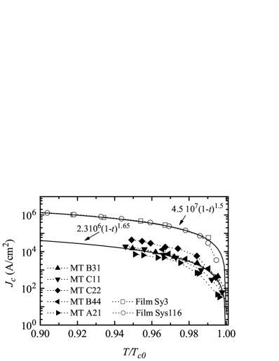
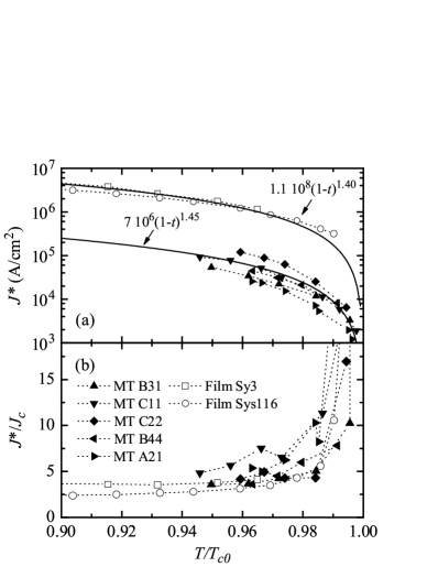
Figure 10(a) summarizes the resultant for our samples. As indicated in this figure, for the melt-textured samples shows a dependence with temperature very close to , which is the same result found in films here, and in other works Currás et al. (2001); Xiao et al. (1998a); Antognazza et al. (2002), for temperatures near . Figure 10(b) shows also that the ratio is very similar for both kinds of samples at any temperature. For temperatures below 0.98 , tends to a temperature independent value between 3 and 5 times (check also Table 1). This result, already reported for films Decroux et al. (2000); Antognazza et al. (2002), is found here to be also common to melt-textured samples.
The unifying trend showed by the ratio would weaken the sometimes implicitly accepted dual causes for the quenching, namely thermal, i.e., nonintrinsic, for massive superconductors, and vortex dynamics or depinning limit, i.e., intrinsic, for films. Indeed, so similar results suggest that the origin of the phenomenon is common for both kind of samples, and this fact can give us some hints about its nature.
Thermal effects are indeed present on our CVCs. On general grounds, however, the very different thermal conditions for films and monoliths work against the thermal origin of the quenching. As mentioned in the introduction, the thermal interchange with the surroundings is much better in thin films than in melt-textured samples. Due to the low heat transfer coefficient of YBCO with liquid nitrogen (0.1-1 W/cm2K Tournier et al. (2000); Mosqueira et al. (1993)), electric power dissipation for massive samples, at the millisecond scale, takes place practically adiabatically. On the other hand, for films, the heat transfer coefficient with the SrTiO3 substrate is around 700-1000 W/cm2K Gupta et al. (1993); Xiao et al. (1998a), favoring a fast heat diffusion. In fact, the low dependence of on the total time of the pulse above around 1 ms,Doettinger et al. (1994); Xiao et al. (1999) and the stability of at constant applied, during tens or hundreds of milliseconds Currás et al. (2001), support that, in our experimental conditions, a quasi steady state is reached in films, even very near .
Note also that the dissipated power density is, in average, nearly four orders of magnitude higher in films than in monoliths, as easily computed from Figs. 4 and 5. Furthermore, the results for thin films have been proved to be quite independent of thermal conditions, as our two samples studied have very similar and values in spite of the different experimental environments and procedures (same result was also obtained by other groupsXiao and Ziemann (1996)). In all, there seems to be too many relevant differences in their thermal environment to easily ascribe the convergence of onto a single curve shown in Fig. 10(b) to only thermal effects.
Notwithstanding, in both kind of samples (thin films and bulks) thermal effects indeed influence our CVCs. For instance, we have already mentioned the sensitivity of the CVCs of melt-textured samples to the current pulse characteristics for current near , giving a variability of a few tens per cent; certainly these differences are attributable to thermal causes. It is likely that thermal effects together with other source of extrinsic effects as sample inhomogeneity could justify the relatively high data scattering in Fig. 10 (more precisely, data scattering would be compatible with heating effects contributing of the order of 50% the total magnitude). Of course, only a thorough study on the thermal dynamics can put in more precise figures on the thermal effects on the quenching. Anyhow, any convincing model given to explain the quenching phenomenon should account for the similar results found in this work for YBCO melt-textured samples and thin films, despite their different environment conditions.
IV Conclusions
Current-Voltage Characteristics (CVCs) of YBa2Cu3O7-δ melt-textured samples and films have been measured at several temperatures close to . In order to minimize heating effects, a pulse technique was used, and refrigeration conditions were optimized by using a pressurized cryostat so that samples were always submerged in liquid nitrogen at any temperature.
From the comparison of both sets of curves, we found an overall common behavior: at low enough applied current a region of zero resistance is observed, followed by a non-linear – curve of low dissipation, and, finally, after an abrupt increase in the resistance of the sample, a highly dissipative region of nearly ohmic behavior is reached.
We have found that the CVCs for both kind of samples share the same features, apart from approximately a factor both in and values. Thus, a simple theoretical expression, namely a critical power law, has been found to reproduce the pre-quenching dissipative region of the CVCs at different temperatures, with almost the same exponent and amplitude’s temperature dependence. The crossover current densities, (critical current density) and (quench current density), are also found to follow the same dependence on temperature. More importantly, in spite of the difference of almost two orders of magnitude between their values in bulk samples and films, their ratio is observed to collapse onto a single temperature dependent curve, common to both kinds of samples. These findings point to an common origin of the CVC behavior in films and melt-textured samples including the quenching, despite the usual different treatment in the literature.
We have also described the very dissimilar role that thermal coupling, shape and thermal inertia are to play on the current-induced heating of bulks and films, suggesting that the final common cause of the quenching phenomenon is primarily intrinsic. The measured fine-scale behavior of can however be modulated by thermal effects.
Further evidence on this conclusion relies on working out some associated issues. In particular, how to bound thermal effects on the observed CVCs? Likely, finite element analysis would help ascertain whether heating accounts for the wide data scattering of the “universal” ratio . Secondly, despite the progress towards a common descriptive frame for superconducting monoliths and films reported here, the two-orders-of-magnitude difference in both current density and electric field amplitudes is demanding an explanation. For instance, why are the or the values so different but not their ratio? The study of these issues, including the influence of the current distribution in the samples, likely to be dependent on the CVCs regimes, is presently under way.
Acknowledgements.
This work has been financed by the CICYT (MAT2001-3053 and MAT2001-3272), Unión Fenosa (contract no. 0666-2002) and Xunta de Galicia (PGIDIT01-PXI20609-PR, PGIDIT02-PXI20610-PN and PGIDIT02-PXI20609-PN). MTG wishes to acknowledge Prof. D. A. Cardwell and his group for their hospitality in the IRC in Superconductivity at Cambridge University, and their invaluable help in getting familiar with melt-texture synthesis techniques.References
- Blatter et al. (1994) See, e. g., G. Blatter, M. V. Feigel’man, V. B. Geshkenbein, A. I. Larkin, and V. M. Vinokur, Rev. Mod. Phys. 66, 1125 (1994).
- Tinkham (1996) See, e. g., M. Tinkham, Introduction to superconductivity (McGraw-Hill, New York, 1996), 2nd ed.
- Samoilov et al. (1995) A. V. Samoilov, M. Konczykowski, N.-C. Yeh, S. Berry, and C. C. Tsuei, Phys. Rev. Lett. 75, 4118 (1995).
- Klein et al. (1985) W. Klein, R. P. Huebener, S. Gauss, and J. Parisi, J. Low Temp. Phys. 61, 413 (1985).
- Lefloch et al. (1999) F. Lefloch, C. Hoffmann, and O. Demolliens, Physica C 319, 258 (1999).
- Currás et al. (2001) S. R. Currás, P. Wagner, M. Ruibal, J. Viña, M. R. Osorio, M. T. González, J. A. Veira, J. Maza, and F. Vidal, Supercond. Sci. Technol. 14, 748 (2001).
- Xiao and Ziemann (1996) Z. L. Xiao and P. Ziemann, Phys. Rev. B 53, 15265 (1996).
- Xiao et al. (1998a) Z. L. Xiao, E. Y. Andrei, and P. Ziemann, Phys. Rev. B 58, 11185 (1998a).
- Doettinger et al. (1994) S. G. Doettinger, R. P. Huebener, R. Gerdemann, A. Kühle, S. Anders, T. G. Träuble, and J. C. Villégier, Phys. Rev. Lett. 73, 1691 (1994).
- Doettinger et al. (1995) S. G. Doettinger, R. P. Huebener, and A. Kühle, Physica C 251, 285 (1995).
- Antognazza et al. (1999) L. Antognazza, M. Decroux, N. Musolino, J.-M. Triscone, P. Reinert, E. Koller, S. Reymond, M. Chen, W. Paul, and Ø. Fischer, J. Low Temp. Phys. 117, 1543 (1999).
- Decroux et al. (2000) M. Decroux, L. Antognazza, N. Musolino, J. Triscone, P. Reinert, E. Koller, S. Reymond, and Ø. Fischer, Physica B 284-288, 2089 (2000).
- (13) J. Chiaverini, J. N. Eckstein, I. Bozovic, S. Doniach, and A. Kapitulnik, cond-mat/0007479.
- Xiao et al. (1998b) Z. L. Xiao, P. Voss-de Haan, G. Jakob, and H. Adrian, Phys. Rev. B 57, 736 (1998b).
- Xiao et al. (1999) Z. L. Xiao, P. Voss-de Haan, G. Jakob, T. Kluge, P. Haibach, H. Adrian, and E. Y. Andrei, Phys. Rev. B 59, 1481 (1999).
- Reymond et al. (2002) S. Reymond, L. Antognazza, M. Decroux, E. Koller, P. Reinert, and Ø. Fischer, Phys. Rev. B 66, 014522 (2002).
- Larkin and Ovchinnikov (1976) A. I. Larkin and Y. N. Ovchinnikov, Sov. Phys. JETP 41, 960 (1976).
- Bezuglyj and Shklovskij (1992) A. I. Bezuglyj and V. A. Shklovskij, Physica C 202, 234 (1992).
- Skocpol et al. (1974) W. J. Skocpol, M. R. Beasley, and M. Tinkham, J. Appl. Phys. 45, 4054 (1974).
- Gurevich and Mints (1987) A. V. Gurevich and R. G. Mints, Rev. Mod. Phys. 59, 941 (1987).
- Skokov and Koverda (1993) V. N. Skokov and V. P. Koverda, Cryogenics 33, 1072 (1993).
- Jelila et al. (1998) F. S. Jelila, J.-P. Maneval, F.-R. Landan, F. Chibane, A. Marie-de Ficquelmont, L. Méchin, J.-C. Villégier, M. Aprili, and J. Lesueur, Phys. Rev. Lett. 81, 1933 (1998).
- Maneval et al. (2001) J.-P. Maneval, F. Boyer, K. Harrabi, and F.-R. Ladan, Journal of Superconductivity 14, 347 (2001).
- Porcar et al. (1998) L. Porcar, D. Bourgault, X. Chaud, J. G. Noudem, O. Belmont, P. Tixador, J. M. Barbut, M. Barrault, and R. Tournier, Mater. Sci. Eng. B53, 189 (1998).
- Tixador et al. (2000) P. Tixador, X. Obradors, R. Tournier, T. Puig, D. Bourgault, X. Granados, J. M. Duval, E. Mendoza, X. Chaud, E. Varesi, et al., Supercond. Sci. Technol. 13, 493 (2000).
- Tournier et al. (2000) R. Tournier, E. Beaugnon, O. Belmont, X. Chaud, D. Bourgault, D. Isfort, L. Porcar, and P. Tixador, Supercond. Sci. Technol. 13, 886 (2000).
- Yang et al. (1999) C. Yang, O. Miura, D. Ito, M. Morita, and T. Tokunaga, IEEE Trans. Appl. Supercond. 9, 1339 (1999).
- Morita et al. (1999) M. Morita, T. Tokunaga, C. Yang, O. Miura, and D. Ito, IEEE Trans. Appl. Supercond. 9, 1316 (1999).
- Morita et al. (2000) M. Morita, O. Miura, and D. Ito, Supercond. Sci. Technol. 13, 896 (2000).
- Herrmann et al. (1997) P. F. Herrmann, E. Beghin, J. Bock, C. Cottevieille, A. Lireche, and T. Verhaege, IOP. EUCAS 97 167, (1997).
- Elschner et al. (1999) S. Elschner, J. Bock, G. Brommer, and L. Cowey, Appl. Supercond. 167, 1029 (1999).
- Tixador et al. (1999) P. Tixador, L. Porcar, D. Bourgault, X. Chaud, and R. Tournier, Cryogenics 39, 77 (1999).
- Lazard et al. (2002) G. Lazard, P. Mathieu, B. Plaçais, J. Mosqueira, Y. Simon, C. Guilpin, and G. Vacquier, Phys. Rev. B 65, 064518 (2002), and references there in.
- Solovjov et al. (1994) V. F. Solovjov, V. M. Pan, and H. C. Freyhardt, Phys. Rev. B 50, 13724 (1994).
- Gao et al. (1991) L. Gao, R. L. Meng, Y. Y. Xue, P. H. Hor, and C. W. Chu, App. Phys. Lett. 58, 92 (1991).
- Yang et al. (1992) Y. Yang, C. Beduz, Z. Yi, and R. G. Scurlock, Physica C 199, 23 (1992).
- Elschner et al. (1994) M. B. S. Elschner, S. Gauss, and W. Assmus, App. Phys. Lett. 64, 2022 (1994).
- Hettinger et al. (1989) J. D. Hettinger, A. G. Swanson, W. J. Skocpol, J. S. Brooks, J. M. Graybeal, P. M. Mankiewich, R. E. Howard, B. L. Straughn, and E. G. Burkhardt, Phys. Rev. Lett. 62, 2044 (1989).
- Gupta et al. (1993) S. K. Gupta, P. Berdahl, R. E. Russo, G. Briceño, and A. Zettl, Physica C 206, 335 (1993).
- Cao et al. (1997) X. W. Cao, Z. H. Wang, J. Fang, X. J. Xu, and K. B. Li, J. Appl. Phys. 81, 7392 (1997).
- Wang et al. (2000) Z. H. Wang, H. Zhang, and X. W. Cao, Physica C 337, 62 (2000).
- Cardwell (1998) D. A. Cardwell, Mater. Sci. Eng. B53, 1 (1998).
- Lo et al. (1996) W. Lo, D. A. Cardwell, C. D. Dewhurst, and S.-L. Dung, J. Mater. Res. 11, 786 (1996).
- Endo et al. (1996) A. Endo, H. S. Chauhan, Y. Nakamura, and Y. Shiohara, J. Mater. Res. 11, 1114 (1996).
- Neal et al. (1991) M. J. Neal, D. B. Chandler, L. J. Klemptner, and M. V. Parish, IEEE Trans. Appl. Supercond. 1, 175 (1991).
- Lepropre et al. (1993) M. Lepropre, I. Monot, M. P. Delamare, M. Hervieu, C. Simon, J. Provost, G. Desgardin, D. Raveau, J. M. Barbut, D. Dourgault, et al., Cryogenics 34, 63 (1993).
- Svistunov et al. (1998) V. M. Svistunov, V. Y. Tarenkov, A. I. D’yachenko, O. Chernyak, and R. Aoki, Physica C 303, 177 (1998).
- Ekin (1993) J. W. Ekin, Processing and Properties of High-Tc superconductors (S. Jin, Singapore, 1993), chap. 9.
- Maehata et al. (1999) K. Maehata, T. Taino, M. Mizokami, K. Ishibashi, M. Takeo, T. Mito, A. Iwamoto, S. Yamada, S. Satoh, O. Motojima, et al., IEEE Trans. Appl. Supercond. 9, 1281 (1999).
- Díaz et al. (1997) A. Díaz, J. Maza, and F. Vidal, Phys. Rev. B 55, 1209 (1997).
- Porcar et al. (1997) L. Porcar, D. Bourgault, J. M. Barbut, M. Barrault, P. Germi, and R. Tournier, Physica C 275, 293 (1997).
- Xiao and Ziemann (1997) Z. L. Xiao and P. Ziemann, Physica C 282-287, 2363 (1997).
- Prester (1998) M. Prester, Supercond. Sci. Technol. 11, 333 (1998).
- Antognazza et al. (2002) L. Antognazza, M. Decroux, S. Reymond, E. de Chambrier, J.-M. Tiscone, W. Paul, M. Chen, and Ø. Fischer, Physica C 372-376, 1684 (2002).
- Mosqueira et al. (1993) J. Mosqueira, O. Cabeza, M. François, and F. Vidal, Adv. Cryog. Eng. pp. 285 – 290 (1993).