0pt0.4pt 0pt0.4pt 0pt0.4pt
Elasticity-Driven Nanoscale Electronic Structure in Superconductors
Abstract
The effects of long-range anisotropic elastic deformations on electronic structure in superconductors are analyzed within the framework of the Bogoliubov-de Gennes equations. Cases of twin boundaries and isolated defects are considered as illustrations. We find that the superconducting order parameter is depressed in the regions where pronounced lattice deformation occurs. The calculated local density of states suggests that the electronic structure is strongly modulated in response to lattice deformations, and propagates to longer distances. In particular, this allows the trapping of low-lying quasiparticle states around defects. Some of our predictions can be directly tested by STM experiments.
pacs:
74.25.Jb, 74.50.+r, 74.81.-g, 74.72.-hIn many complex electronic materials such as cuprates, manganites, ferroelastic martensites, and titanates, unexpected and puzzling multiscale modulations of charge, spin, polarization, and strain variables have been revealed by high resolution microscopy Multi1 . The nonuniform textures found in these doped materials indicate that their origin is intrinsic: they arise from coupling between various degrees of freedom. The textures fundamentally affect local and mesoscopic electronic, magnetic and structural properties, which are central to the functionality of correlated electronic materials. There is ample evidence for significant coupling amongst the electronic degrees of freedom with the lattice distortion in cuprates and manganites. The charge carrier doping can act as a local stress to deform surrounding unit cells Multi1 ; Ahn02 . We might employ a Landau-Ginzburg (LG) theory to study the coupling between the electronic (Cooper pair) and lattice (strain tensor) degrees of freedom in superconductors. However, the LG theory can only describe the long wavelength behavior. The local electronic properties and lattice distortion necessitate a treatment at the atomic scale. Recently, we have developed an atomic scale theory for determining lattice distortions by using strain related variables and their constraint equations Ahn02 . This now enables a systematic study of the influence of strain on electronic wavefunctions. Here we apply a microscopic theory to study the order parameter and local quasiparticle properties in both and -wave superconductors.
We consider the following model on a square lattice:
| (1) | |||||
Here annihilates an electron of spin on site . The quantities and are the on-site impurity potential (if any) and the chemical potential, respectively. The hopping integral is modified by the lattice distortion. The electron-lattice coupling is approximated by , where is the bare hopping integral, is the lattice-distortion variable, and is the coupling constant. In our nearest neighbor realization, the bare hopping integral is for nearest neighbor sites and zero otherwise. Specifically, we take the form of the lattice distortion to be: , where are the undistorted lattice coordinates and the lattice displacement vectors with respect to . We assume an effective superconducting gap function given by , where (i.e., attractive Hubbard- model) for -wave superconductivity and (with specifying the nearest neighbors to the -th site) for -wave superconductivity. By performing a Bogoliubov-Valatin transformation, we may diagonalize our Hamiltonian by solving the Bogoliubov-de Gennes (BdG) equation deGennes89 :
| (2) |
subject to the self-consistency conditions for the superconducting (SC) order parameter (OP):
| (3) |
Here the single particle Hamiltonian reads . The quasiparticle wavefunction, corresponding to the eigenvalue , consists of electron () and hole () amplitudes. The quasiparticle energy is measured with respect to the chemical potential.
We solve the BdG equations self-consistently by starting off with an initial gap function. After exactly diagonalizing Eq. (2), the obtained wavefunction is substituted into Eq. (3) to compute a new gap function. We then use this as an input to repeat the above procedure until a desired convergence is achieved. Below, we report our results for two types of local lattice distortions at zero temperature— a superlattice formed by twin boundaries and a single defect. We measure the length and energy in units of (the undistorted lattice constant) and . The chemical potential and no extrinsic impurity scattering is introduced (). The pairing interaction for both the -wave () and -wave () superconductors is taken to be 3. The typical system size is and periodic boundary conditions are applied. When the local quasiparticle density of states (LDOS) is computed, we implement a much larger system using the above small system as a supercell. In the absence of distortions, Eq. (2) is readily solved by resorting to translational invariance: the resulting quasiparticle energy with , and the energy gap or for the or -wave superconductor respectively. For the given parameter values, we obtain and . In both cases, the superconducting coherence length is . These values are exaggerated when compared to real materials: The choice of values is motivated by the desire to enhance the effect of the lattice distortions.
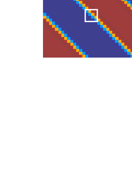
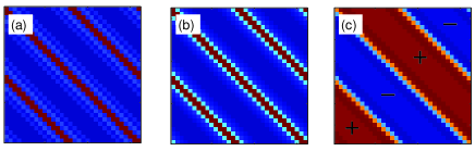
Before proceeding to the BdG calculation sketched above, we generate (following Ahn02 ) two atomic scale lattice distortions. These distortions arise from long-range anisotropic interactions between strains to maintain the compatibility constraints. The (square to rectangle) strain mode for a periodic twinned microscopic structure and the corresponding atomic displacements are depicted in Fig. 1(a-b). The domain consists of rectangular distortion (red and blue) separated by a domain wall where . Note that similar but more “realistic” microstructures have also been obtained using Monte Carlo techniques Goldman95 . Similar quantities for a single defect are displayed in panels (c-d). Near the defect, four alternating distortions are formed in (clover leaf) “-wave like” pattern.
In Fig. 2, we show the spatial variation of the SC OP induced by the deformation of Fig. 1(a) in both and -wave superconductors. In both types of superconductors, the OP is lowered within the domain and is elevated at the domain wall (Fig. 2(a-b)). The magnitude of the OP is depressed in comparison to an undistorted square lattice since the lattice deformation changes the band structure, leading to a reduction in normal density of states at the Fermi energy. Even at the domain wall, where the strain induced deformation is weakest, the amplitude of the enhanced OP is smaller than its value in an undistorted square lattice. This is due to the confinement from the two neighboring domains. In an -wave superconductor, the relative orbital motion between two paired electrons has an angular momentum , which has the highest symmetry and generates no subdominant OPs with lower symmetries. However, for a -wave superconductor, the relative motion between two paired electrons has the angular momentum , which upon scattering from any inhomogeneity can generate a subdominant OP with symmetry not lower than that of . The -wave OP is defined by , whereas the extended -wave OP is . In a twinned domain of a -wave SC, a subdominant extended -wave component is generated in a real combination . Because the symmetries of two twinned domains are reflected into each other with respect to the twin boundary, the relative phase between the - and -wave components switches by when a twin boundary is crossed (Fig. 2(c)). It has been argued phenomenologically Multi5 that a local time-reversal-symmetry-breaking state exists at a twin or grain boundary of YBa2Cu3O7-δ. Within numerical accuracy, our result shows a real admixture of the -wave and -wave components of the OP. A pairing state was also found at the -oriented surface or interface of a -wave superconductor in early work Multi2 . A crucial difference between the twin boundary of Fig. 2 and the -oriented surface of earlier work is that the dominant -wave component reaches a maximum at twin boundaries, whereas it is strongly suppressed at the -oriented surface or interface. Experimentally, the existence of a time-reversal-symmetry-breaking pairing state in high- cuprates is the subject of current debate Multi3 .
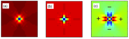
As another example, we show in Fig. 3 the spatial variation of the superconducting OP around the single defect (Fig. 1(c)) in both the -wave and -wave superconductor cases. The OP is depressed at the center of the defect, and reaches its defect-free bulk value at the length scale . Notice that for a lattice-deformation defect, which affects the local electron hopping integral, the OP has a minimum at four sites surrounding the defect center. It is different from the case of an externally substituted unitary impurity, where the minimum of OP is located only at the impurity site itself Zhu00 . The range of influence of such a defect can be very large depending on the strength of electron-lattice coupling— the elasticity propagates the electronic response. The -wave energy gap has a sign change at the nodal directions of the essentially cylindrical Fermi surface, but the -wave OP does not exhibit such a sign change in real space. When the defect is introduced, an extended -wave component of the OP is induced when the dominant -wave component is depressed at the defect. Strikingly, the induced -wave component has a sign change across the diagonals of the square lattice, i.e., , where is the azimuthal angle with respect to the crystalline axis. This is a direct manifestation of the -wave pairing symmetry in real space. This feature can be understood from a phenomenological LG free-energy density functional with a two-component SC OP: , where we take to be always positive while such that there exists only a single transition into a -wave pairing state in a homogeneous system. When a defect is introduced, the -wave component is depressed. Since the -wave component itself should be very small, the term is only a higher-order correction. Therefore, it is the mixed-gradient term that induces the -wave component and also determines the relative phase to be or . The sign change is also evident by exchanging the and components of the position coordinate in the mixed-gradient term.
Once the self-consistency for the order parameter is obtained, we calculate the LDOS:
| (4) |
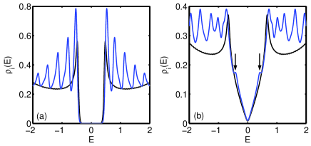
where is the derivative of the Fermi distribution function with respect to the energy. The LDOS determines the differential tunneling conductance, measurable by STM experiments Pan00 . Figure 4 shows the LDOS at a domain wall for both types of superconductors, where the modulation of the superconducting OP forms a superlattice, with its maximum at the domain wall playing the role of an off-diagonal potential barrier ( in Eq. (2)). For an -wave superconductor, the quasiparticles are gapped away with their energy below the minimum SC OP. Outside the minimum of the pair potential, energy bands are formed by the quasiparticle scattering off the off-diagonal energy barriers at the domain walls. Except for the gap about the Fermi energy (), this is reminiscent of the electronic structure in semiconductor superlattices (e.g., alternating GaAs/GaAlAs layers). Interestingly, the bottom of the oscillation pattern follows the LDOS (black line) of a system formed by a single rectangular domain. Similar oscillations are obtained for the -wave superconductor. However, the bottom of the oscillations do not follow the single domain DOS (black line). In addition, weak subgap peaks (labeled by arrows in Fig. 4(b)) appear symmetrically in the LDOS on the domain wall but are absent in the single-domain LDOS. We speculate that these resonant states are due to the gradient of the -wave gap component induced inside the domain.
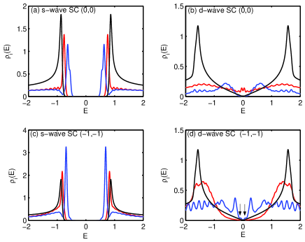
As shown in Fig. 5, we have also calculated the LDOS near the center of a single defect. The depression of the SC OP at the defect makes a quantum-well-like profile of the energy gap. The size and depth of the well is determined by the electron-lattice coupling constant. Because of the difference between the -wave and -wave pairings, the -wave potential well is closed everywhere, whereas the -wave well has four slits along the diagonals of the square lattice. In the -wave superconductor, the well is shallow and small for weak coupling, which cannot trap low-lying quasiparticle bound states; for strong coupling constants, the well is deep and large so that subgap quasiparticle bound states are induced (the red and blue lines of Fig. 5(a) and (c)). The energy of these low-lying states must be inbetween the bottom and edge of the well. Therefore, it is notable that the energy of these subgap states is shifted toward the Fermi surface as the electron-lattice coupling is increased (the blue line in Fig. 5(a) and (c)). The situation here is also different from an -wave vortex core, where the OP at the core center must vanish such that the low-lying bound states are always trapped Multi4 . The electronic structure at the defect in a -wave superconductor becomes even richer: For (weak coupling as compared to the band width of the non-deformed square lattice), the lattice distortion plays the role of a weak defect for the quasiparticle scattering. In this case, a resonant peak with a dip exactly at the Fermi energy is seen (the red line in Fig. 5(b)). The overall peak comes from the scattering of quasiparticles off the single-particle off-diagonal potential (i.e., local change of the hopping integral as a response to the lattice deformation). This lattice-deformation induced resonance state also exhibits Friedel oscillations. Typically, the peak structure appears in the LDOS at (0,0) (We label the four sites surrounding the defect center by (0,0), (1,0), (1,1), (0,1)) and (-2,-2). In contrast to the case of an extrinsic on-site potential-scattering impurity Balatsky95 , the LDOS spectrum is symmetric since even the local particle-hole symmetry is preserved here. For (strong coupling), the -wave OP is almost fully depressed (less than 0.03), while the maximum of the induced -wave OP reaches 0.085. The local off-diagonal potential becomes more finite ranged, which causes a local change of the band width. The ‘resonant’ peaks are pushed to higher energies () (the blue line of Fig. 5(d)). Furthermore, small shoulders appear close to the Fermi energy (the blue lines of Fig. 5(b) and (d)), which are precursors of new Andreev resonance states. We have also computed the LDOS without imposing self-consistency on the OP and found that the double-peak structure is V-shaped with no existence of the shoulders. This leads us to speculate that the new Andreev resonance states come from the confinement of the induced -wave OP. However, these states are still delocalized because the quasiparticles can leak out of the well through the slits along the diagonal directions where the induced -wave component vanishes. All these features are unique to an elastic defect in a -wave superconductor with short coherence length.
In conclusion, we studied the effects of elastic lattice deformation on the nanoscale electronic structure in superconductors. We have shown that the SC OP is depressed in the regions where the lattice deformation exists. The calculated LDOS suggests that the electronic structure is strongly modulated in response to the lattice deformation. In particular, it is possible to trap low-lying quasiparticle states around the defects. Images of these states will manifest the underlying long-range anisotropic lattice deformation. These predictions can be directly tested by STM experiments in new functional superconducting materials. Our approach is readily extended to other elastic textures and SC symmetries. Self-consistent coupling of the elastic and SC textures on an equal footing will be pursued elsewhere. It would also be interesting to study the electronic response by using Monte Carlo generated microstructures as input, which constitutes future work.
We thank A. Saxena and S. R. Shenoy for useful discussions. This work was supported by the US Department of Energy through the Los Alamos National Laboratory.
References
- (1) For a review, see Lattice Effects in High- Superconductors, eds. Y. Bar-yam, T. Egami, J. Mustre-de Leon, and A. R. Bishop (World Scientific, Singapore, 1992); Nanoscale Phase Separation and Colossal Magnetoresistence, ed. E. Dagotto (Springer, New York, 2003); Instrinsic Multiscale Structure and Dynamics in Complex Electronic Oxides, eds. A. R. Bishop, S. R. Shenoy, and S. Sridhar (World Scientific, Singapore, 2003).
- (2) K. H. Ahn et al., cond-mat/0207224 (unpublished); A. R. Bishop et al., cond-mat/0304198 (unpublished).
- (3) P. G. de Gennes, Superconductivity of Metals and Alloys (Addison-Wesley, New York, 1989).
- (4) M. Goldman et al., Phil. Mag. Lett. 70, 65 (1994); Phys. Rev. B 52, 1331 (1995).
- (5) M. Sigrist, D. B. Bailey, and R. B. Laughlin, Phys. Rev. Lett. 74, 3249 (1995); M. B. Walker, Phys. Rev. B 53, 5835 (1996); A. B. Kuklov and M. Sigrist, Int. J. Mod. Phys. B 11, 1113 (1997).
- (6) M. Matsumoto and H. Shiba, J. Phys. Soc. Jpn. 64, 3384 (1995); 64, 4867 (1995); M. Fogelström, D. Rainer, and J. A. Sauls, Phys. Rev. Lett. 79, 281 (1997); J.-X. Zhu, B. Friedman, and C. S. Ting, Phys. Rev. B 59, 3353 (1999). Y. Tanuma et al., ibid. 60, 9817 (1999).
- (7) K. A. Kouznetsov et al., Phys. Rev. Lett. 79, 3050 (1997);
- (8) M. Covington et al., ibid. 79, 277 (1997); J. Y. T. Wei et al., ibid. 81, 2542 (1998); Y. Dagan and G. Deutscher, ibid. 87, 177004 (2001); W. K. Neils and D. J. Van Harlingen, ibid. 88, 047001 (2002).
- (9) J.-X. Zhu et al., Phys. Rev. B 61, 8667 (2000).
- (10) See, e.g., S. Pan et al., Nature 403, 746 (2000).
- (11) A. V. Balatsky, M. I. Salkola, and A. Rosengren, Phys. Rev. B 51, 15547 (1995).
- (12) C. Caroli, P. G. de Gennes, and J. Matricon, Phys. Lett. 9, 307 (1964); H. F. Hess et al., Phys. Rev. Lett. 62, 214 (1989); F. Gygi and M. Schluter, ibid. 65, 1820 (1990).