Relevance of the EEL spectroscopy for in-situ studies of the growth mechanism of copper-phthalocyanine molecules on metal surfaces: Al(100)
Abstract
Reflection electron energy loss spectroscopy (EELS) in specular and off specular geometry has been employed to study the early stage of the copper phthalocyanine (CuPc) growth on Al (100) substrate. EEL spectroscopy has been a useful tool in order to study electronic structure of molecular films also in the submonolayer regime. The electronic structure of the first deposited layer of CuPc is strongly influenced by charge transfer from the Al substrate to the lowest unoccupied molecular orbital (LUMO). The strong molecule-substrate interaction gives rise to a coverage dependent frequency shift of the Al surface plasmon. Successive layers have essentially the electronic structure of the molecular solid. Momentum resolved EELS measurements reveal that, in the case of the thicker film investigated (22 Å), the plane of the molecule is almost perpendicular to the surface of the substrate.
pacs:
73.22.-f, 73.20.Mf, 79.20.UvI Introduction
Metal phthalocyanines, denoted MPc (Pc = phtalocyanine C32H16N8), have been synthesized using elements from any group of the periodic table. They are planar molecules, closely related to biological molecules such as porphyrins, constituted by a porphyrazin ring (porphyrin-like) bonded to four benzene rings. Main features of this class of molecules are a metal atom in the center (usually one of the first transition series) and an extended -electron delocalization. MPc exhibit an high chemical and thermal stability and exist in different forms; among the various polymorphs Leznoff and Lever (1989), the and ones are the best known and the most widely studied. In both crystalline forms the phthalocyanine units are positioned in columnar stacks with the ring tilted with respect to the stacking axis (tilt angle), which cohere to form the molecular crystal. The two forms display identical interplanar distance (3.4 Å) consistent with a Van der Waals bond, but they differ for the tilt angle: in the form and in the form. Furthermore their lattice parameters are different (23.9 Å in the form and 19.6 Å in the form) as well metal-metal distance. The different aggregation geometry results in changes of the electrical conductivity along the stacking direction. From an electronic point of view, MPc are semiconductors whose gap width depends on the central atom (typically 1.5- 1.8 eV) and slightly on the geometrical arrangement (a variation of 60-70 meV between the and form in the absorption spectra has been observed Lucia and Verderame (1968)). After p-doping by oxidizing agents and stabilization of a face to face stacking Canadell and Alvarez (1984), MPc become electrical conductors thus enlarging their field of applications. All these properties allow several technological applications in different fields such as non-linear optics, molecular electronics and highly specific gas-sensors fabrication (such as NO2 Dogo et al. (1992a, b)). Therefore the knowledge of MPc spatial and electronic structure, both as bulk crystals and as adsorbates on well-defined substrates, is much relevant. Over the past decade MPc overlayers have been studied interfaced with metals Tokito et al. (1994); Smolyaninov (1996); Dufour et al. (1994); Walzer and Hietschold (2001) semiconductors Dufour et al. (1994, 1995); Cox et al. (1999a, b) and layered compounds Ottaviano et al. (1997); Shimada et al. (1998); Walzer and Hietschold (2001). Attempts have been made to grow them in an ordered manner (heteroepitaxy) on various substrates, some of them of high technological interest Koma (1992); Tada et al. (1992). Substrate materials which have been shown to support the epitaxial growth of phthalocyanine ultrathin films now include single crystal metals, layered semiconductors (SnS2, MoS2, HOPG), surface-passivated three dimensional semiconductors (Si, GaAs, GaP), and insulators such as freshly cleaved single crystal halide salts Leznoff and Lever (1996). In some cases an overgrowth evolution characterized by different molecular orientations has been observed. In particular, the adsorption starts with planar arrangement at low coverages, when substrate-molecule interaction is believed to dominate, to change into out-of-plane orientation at higher coverages where molecule-molecule interaction is expected to become relevant Poirier and Pylant (1996).
Recently, substrate surface reconstruction has been observed induced by molecular deposition and it has been speculated that it might be determined by strong molecule-substrate interaction. In particular, for CuPc/Ag(110) interface, the Ag surface reconstruction has been ascribed to the presence of facets Bohringer et al. (1997). More recently, for gold (110) surface has been detected a clear long range reordering of the substrate due to adsorption of CuPc Evangelista et al. (submitted). The capability of -conjugated molecules to induce displacements of surface atoms in conjunction with self-organised molecular growth Yokoyama et al. (2001) appears then to be a general characteristic that is relevant from a technological point of view and makes adsorption of this class of molecules, in perspective, an attractive option for nano manipulation of surfaces Joachim et al. (2000).
Among metals aluminum represents the archetypal for nearly-free-electron systems; therefore the Al surface constitutes an interesting alternative to the more extensively investigated transition metal substrates. In particular the absence of occupied orbitals might highlight the role played by localization of the states in influencing the electronic structure of an organic-inorganic interfaces. To the best of our knowledge Al surface has never been studied as substrate for CuPc films deposition, apart from the case in which it was used to support thick films of CuPc. In this latter case, the aim was to analyze bulk interband molecular transitions Scrocco et al. (1993) and the influence from the metal-molecule interface was not investigated.
The aim of this work is to study the growth mode and the molecular orientation of the overgrown film as a function of its thickness, and to characterize the geometric and electronic structure of monolayer and submonolayer CuPc films, deposited by thermal evaporation on an Al(100) substrate. CuPc is a dye pigment thermally very stable, thus allowing purification by sublimation technique and deposition by thermal evaporation or organic molecular beam epitaxy (OMBE) Leznoff and Lever (1996). Electron energy loss spectroscopy (EELS) performed both in reflection geometry and as a function of the ejection angle are the main spectroscopic tools applied in this work.
The literature reports on a limited number of EELS experiments on MPc films in general and on CuPc films in particular, most of them made in transmission geometry on thick films, with high primary electron energy. Low energy electron energy loss spectra in reflection conditions have been measured on policrystalline films of H2Pc, CuPc, VOPc and PbPc Tada et al. (1989); Bubnov and Frankevich (1974), (prepared by sublimation under high vacuum mbar) on a Si substrate, with a primary electron energy of 100 eV. The spectra of all phthalocyanine complexes examined have similar structures and the observed peaks in the excitations region are always in good agreement with the correspondent optical absorption data Lucia and Verderame (1968); Schechtman and Spicer (1970).
Although a limited number of works have made use of EEL spectroscopy to study MPc films, this technique is particularly attractive because it allows to examine an energy range corresponding to a region ranging from IR to soft X-ray in the electromagnetic spectrum by using a laboratory based spectrometer that can be easily conjugated to a growth chamber for in-situ investigation of the growth mechanism. Main target of this paper is to put in evidence the possibility to monitor the growth of thin films of CuPc, ranging from submonolayer to a few monolayers, by the use of EEL spectroscopy and emphasize the potentiality of EELS technique in measuring the electronic properties of these films. Furthermore, the possibility to determine the orientation of the molecule with respect to the substrate has been shown. The latter result has been reached exploiting the relative orientation of transition dipole moment (i.e. the symmetry of the transition at 3.7 eV) and momentum transferred in the collision. A similar experiment, based on core transition, has already been performed in the case of simpler organic molecule adsorbed on metallic substrate Tyliszczak et al. (1989).
II Experimental
The experiments reported in this paper have been performed at the LASEC laboratory (Dip. di Fisica and Unità INFM, Università Roma Tre) with an apparatus that allows to study thin films, grown in-situ, by a variety of electron spectroscopies, thus providing complementary informations on both electronic and geometric structure of the overlayer. In particular, the apparatus consists of two separate UHV chambers. The experimental chamber, equipped with an electron gun, a x-ray source and two emispherical analyzers, is devoted to spectroscopic investigations. A 5 degrees of freedom sample manipulator allows to control position in space and temperature of the sample. A comprehensive description of this apparatus is given elsewhere Ruocco et al. (1999a).
The preparation chamber features an electron bombardment evaporator Tricon Verucchi and Nannarone (2000) and a quartz crystal microbalance (QCM) used to control the growth rate of the films. The specific nature of CuPc, i.e. the high condensability of the evaporated and its tendency to sublimate forming needle-shaped crystals, made necessary to modify the evaporator source Donzello (2000). The thickness of the molecular overlayer is not univocally determined by the rate of deposition onto the QCM as it depends upon the sticking coefficient and the deposition mode. Hence from the QCM measurements, a nominal thickness, corresponding to uniform coverage of the surface, is deduced. Furthermore, the preparation chamber features an ion gun for sputtering substrates and a magnetically coupled linear feedthrough for transferring samples.
The Al substrate is a single crystal (5 x 5 x 2.5 mm3) with (100) orientation and is supported by a molibdenum sample holder. Two different cleaning procedures have been adopted to remove the thick oxide layer always present on samples stored in air. The Al surface was cleaned by electro polishing prior to introduction in the preparation chamber. The electropolishing was performed on an AB Electropolishing cell, Buchler Std, using a solution constituted of 345 mL of HClO4 60 % and 655 mL of (CH3CO)2O. The sample was then cleaned under vacuum by repeated cycles of sputtering with argon ions (4 keV, 6 7 A) and annealing (450 oC) Musket et al. (1982). The sample cleanliness and order was checked before every deposition by means of AES and EELS . Commercial CuPc was obtained from Aldrich Chemical (97 % dye content); it was purified by sublimation under vacuum (540-550 oC, mbar) and then introduced in the molibdenum crucible of the electron bombardment evaporator. The purity of the powder was checked by elemental analyses for C, H, N, performed by an EA 1110 CHNS-O CE instrument. Calculated for C32H16CuN8: C, 66.72; H, 2.80; N, 19.45. Found: C, 66.58; H, 2.66; N, 19.34 %. (The uncertainty was 0.3 for C and 0.1 for H and N). The molecule was sublimated onto the substrate at room temperature at a rate of approximately 0.5 Å/min. The film, prepared in such a way, has been found stable until 400 oC and under electron bombardment (impinging current of few nA) does not suffer evident radiation damage; in summary it stays clean, under UHV condition, for at least 48 hours. The EEL spectra reported in the paper were collected at room temperature with one of the two emispherical electron analyzers present in the experimental chamber. EELS measurements were performed at fixed incident kinetic energy and the overall energy resolution was 500 meV throughout the whole range of incident electron energies (140 eV to 500 eV); the angular resolution was . Two different kinds of EEL spectra have been recorded in this work. In the first one the energy loss probability is measured in specular reflection conditions with a fixed incident angle of 34∘ from surface normal. In the second one the probability for a given energy loss was measured as a function of the transferred momentum by rotating the sample while keeping fixed the included angle between the incoming and scattered beams.
III Results and discussion
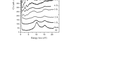
In fig. 1 are reported the constant momentum transfer EEL spectra measured in specular reflection as a function of CuPc coverage, the nominal thickness (from now on coverage) ranges from 1 Å up to 22 Å. All the spectra have been collected in specular reflection geometry and with a primary energy of 140 eV in order to take advantage of the reduced mean free path and then to be sensitive to the molecular film. The EEL spectrum of clean Aluminum is also reported for reference.
III.1 Interface plasmon
The clean Al spectrum is dominated by two structures at 10.5 eV and 15 eV that correspond to the surface (SP) and bulk plasmon (BP), respectively. The intensity of the bulk plasmon drops with increasing coverage and almost disappears already for a coverage of 6 Å. On the contrary the surface plasmon shows a more articulate evolution. For the lowest coverages the centroid of this structure shifts towards lower loss energy; the shift increases as the thickness grows up to 3 Å: in this situation it is not any more possible to resolve the surface plasmon from the molecular transitions appearing in the 5-8 eV region with similar intensity. The evolution of the SP with coverage is more evident in fig. 2, where are reported the EEL spectra on the CuPc/Al(100) system, but with a primary energy of 500 eV, in order to highlight the interface excitations rather than the overlayer ones.
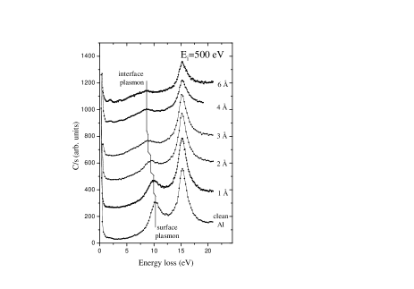
It is then easier to follow the evolution of surface plasmon at very low coverages finding that it shifts toward lower loss energy when increasing the coverage and it reaches a steady value (8.5 eV) already at 4 Å, well before bulk-like conditions are fulfilled. It is therefore plausible to ascribe the SP peak to an interface plasmon such as those observed by Raether Raether (1980) in the case of thin films deposited on metallic substrate. More recently, a peak at 7 eV in the EEL spectrum of an Al surface exposed to O2 has also been attributed to plasma oscillations localized in the metal substrate Hoffman et al. (1988). To ascertain whether or not the observed SP transition corresponds to an interface plasmon, it can be considered that the energy of such a collective mode is expected to disperse with the overlayer thickness unless the following condition is fulfilled Raether (1980):
| (1) |
where is the momentum associated with the plasma oscillation, i.e. the surface component of the momentum exchanged in the inelastic scattering (q), and is the thickness of the film. Dispersion of the plasma frequency as a function of the thickness of the overlayer, was already observed for a thick Al film (150 Å) covered with oxide layer Kloos (1968). In our case can be evaluated on the basis of the double collision model that is known to be valid Ruocco et al. (1999a, b); Saldin (1988) for the energy loss processes in specular reflection geometry. According to this model, the inelastic scattering is followed or preceded by an elastic one and the inelastic cross section can be assumed different from zero only for scattering angle falling within a cone of aperture where is the energy of primary beam and is the energy lost in the collision. Consequently the maximum allowed is of the order of Å-1 where is the incident momentum. This explains the dispersion of the interface plasmon observed in fig.2, in particular the asymptotic value is reached for a coverage of 4 Å that is the minimum coverage to satisfy inequality 1 ( = 4.8). Moreover, making the assumption that the Al conduction electrons are well described by a free electron gas, the interface plasmon frequency is related to the dielectric constant of the molecular film by the relation Raether (1980):
| (2) |
From the measurements reported in fig.2 we estimate for eV and for eV hence obtaining a value of 2.1 for the dielectric constant of the CuPc, a value that well agrees with those measured for other planar organic molecules, with an extended delocalization of electrons, like benzene. All these finding support the hypothesis that the dispersing structure observed in fig.2 is to be ascribed to a surface plasma wave propagating within the aluminum substrate whose frequency is modified by the dielectric response of the molecular adlayer. To the best of our knowledge this is the first observation of an interface plasmon induced by organic molecule in aluminum.
III.2 Molecular transition
Electronic transitions due to the CuPc molecule become evident in the EEL spectrum starting from a coverage of 3 Å; for this coverage two weak peaks centered at 1.9 and 3.7 eV (hereafter Q and B transitions respectively) appear together with a broad structure between 5 and 8 eV that is more intense than the Q and B transitions. Increasing the coverage, the Q and B transitions are always present: their intensities increase as a function of the coverage while their shape, energy position and relative intensity remain substantially unchanged. On the contrary the broad structure at 5-8 eV shows a modest evolution reaching its final shape at 6 Å. For coverages of this value and higher the structure shows two prominent features located at 5.8 and 7.1 eV that are weaker than the B and Q transitions. It is interesting to note that starting from 10 Å, the EEL spectrum does not show significant modifications, thus suggesting that the molecular film has reached a bulk-like configuration. This is confirmed by the observation that the energies at which electronic transitions appear do correspond to those reported in a previous work on thick CuPc films Tada et al. (1989). According to the diagram level of the CuPc molecule as obtained from the four-orbital model Schaffer and Gouterman (1972); Schaffer et al. (1973); Gouterman (1978), the transitions at lower energies ( eV) appearing in fig.1 are assigned mostly to electronic transitions of phthalocyanine molecules. In particular the peak at 1.9 eV, the Q band, is due to a mixture of and transitions; although the two transitions are almost degenerate in energy, the former has a dipole moment perpendicular to the molecular plane while the latter, mostly due to orbitals from copper atom, has dipole moment in the plane of the molecule. On the contrary the peak at 3.7 eV, the B band, is related to the single transition thus having a well defined symmetry with respect to the plane of the molecule. We also observe peaks at 5.8 eV, C band, and at 7.1 eV, band, both assigned to a transition. It is worth noting that there is a good agreement between the transition observed by means of EELS for the bulk-like coverages (10-22 Å) and those obtained in the optical absorption spectra for thick film of CuPc Schechtman and Spicer (1970). Additionally, in absorption spectroscopy two other bands at 4.7 eV (N) and at 7.8 eV () have been identified. We speculate that the former transition (N) gives rise, in our spectra, to the low energy shoulder of the peak centered at 5.8 eV while the latter transition () is not detectable as already reported in a previous EELS work Tada et al. (1989).
From fig. 1, the Q and B transitions appear for coverages of 3 Å and higher. This threshold value correspond, in the hypothesis of a flat lying adsorption geometry, to saturating the surface with one monolayer. In this framework molecules from the first layer do not contribute to Q and B bands. In order to understand whether at low coverages these structures are simply confused in the background, or an alteration of the electronic structure occurs that forbids them, the Q and the B band intensities are plotted as a function of CuPc coverage (see fig. 3).
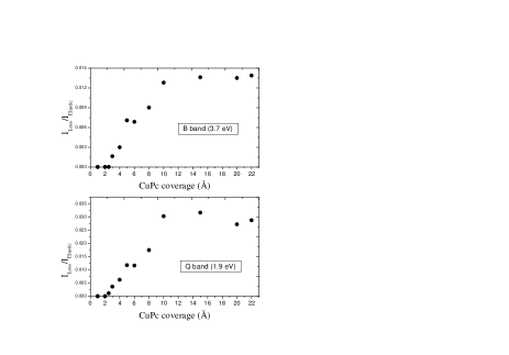
For coverages below 10 Å we observe that the experimental data can be fitted with a straight line whose intercept to zero corresponds to a coverage between 2 and 3 Å. Hence, appearance of the optical absorption bands (Q and B) in the EEL spectrum has a clear threshold at a low non zero coverage. It implies that the electronic structure of the first adsorbed molecules is different from that of the bulk ones. We also notice that the threshold coverage of 2-3 Å is consistent with the saturation value for one layer of flat lying absorbed molecules. This behavior is confirmed by a similar investigation performed at 500 eV of incident energy Donzello (2000). In other words we can make a clear distinction between molecules directly bonded to the Al substrate (coverage below 3 Å) and molecules not directly bonded to the substrate (coverage above 3 Å). In the latter case the electronic structure, as revealed by EELS, is identical to that of bulk CuPc while in the former case modification of the electronic structure is such to prevent transitions toward the LUMO orbital. Above 10 Å we observe a saturation of the Q and B bands intensity. It is now important to understand why the optical transitions are inhibited for molecules directly bonded to the Al substrate. The simplest hypothesis to be made requires that, as a consequence of charge transfer, electrons from the Al substrate fill up the molecular LUMO and the orbitals. In order to fill the LUMO (doubly degenerate) and the states, 5 electron per molecule should migrate from the substrate. Roughly speaking, each CuPc molecule covers about 32 Al atoms, then each of this metallic atoms will contribute with about 0.16 electron to the charge transfer process. Considering the high density of nearly free electrons of the substrate, such a charge transfer is not unreasonable. Besides, a comparably large charge transfer it has already been observed in the case of C60 overlayer grown on Al Hebard (1994). Further support to the charge transfer mechanism comes from considerations on the molecular energy levels. For molecular solids grown on solid surfaces it was commonly assumed that organic- metal interface energy diagram can be obtained by aligning the vacuum levels of the two materials. Recently it has been demonstrated that this assumption is not always true for both metal Hill and Kahn (1998) and semiconductor substrates Hill and Kahn (1999). Vacuum level alignment applies only when the interaction between molecular film and substrate is weak. As previously pointed out this is not our case. The charge transfer with consequent formation of an ionic bond between CuPc and Al substrate implies the formation of a dipole barrier at the interface Hill and Kahn (1999). The presence of a surface dipole barrier is also supported by the consideration that the work function (WF) of aluminum is 4.3 eV while the electron affinity (EA) of the molecule (distance between LUMO and vacuum level) is only 3.1 eV. Then the 1.2 eV difference between the two levels should prevent any charge transfer in the case of non-interacting interfaces. Our EELS analysis suggests that LUMO is filled and then it is either aligned or it lies below the Fermi level; we then conclude that the LUMO state of the molecules directly bonded to the metal shifts at least by 1.2 eV. Similar results have been already observed for C60/Au(110) Maxwell et al. (1994); also in that case the authors claim for a charge transfer from the metal to the molecule even though, in that case, the difference between the EA and WF is as large as 2.67 eV. In conclusion a sizeable charge transfer from substrate to molecule explains the observed threshold in coverage for appearance of optical bands in the EEL spectra.
III.3 EEL spectra as a function of the exchanged momentum
The inelastic scattering in specular reflection geometry can be described by means of the double collision model (DCM) theoretically predicted Saldin (1988) and experimentally verified Ruocco et al. (1999a, b) for energy losses in the range 1030 eV. In this model the measured electrons suffer a double collision (one elastic and one inelastic) with the solid: in the elastic collision electrons are reflected from the surface, and in the inelastic one an energy loss occurs while scattering in forward direction. Concerning our experiment, the proposed model has two main implications: i) the smallness of the momentum exchanged in the inelastic collision, compared with the momentum of the incident electrons, allows to apply the dipole approximation, ii) two channels will incoherently contribute to the total cross section, that in which the elastic collision precedes (D+L) and that in which it follows (L+D) the inelastic collision. As previously pointed out the transitions at the lowest energies have a well defined symmetry; in particular the B band, due to its unambiguous character, has dipole moment () perpendicular to the plane of the molecule. The spatial orientation of the molecule can then be probed by changing, in the experiment, the direction of dipole moment with respect to the momentum transferred in the inelastic collision. In this framework the cross section of EELS is proportional to , thus the molecule orientation can be derived studying the EELS probability of the transition B as a function of the angle included between and .
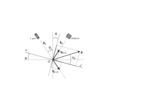
In fig.4 is reported the kinematics of the experiment. According to the DCM, two inelastic exchanged momenta are drawn directed along the directions of the incoming beam () and of the collected beam (). is the angle formed by vector with respect to the surface and it represents the orientation of the molecule. The experiment was performed with the higher coverage (22 Å), by scanning the angle , i.e. the angle between the normal to the surface and the bisector of the included angle between incoming and outgoing electron beams (see fig.4). The directions of incident and diffracted beams are fixed in the laboratory reference frame, thus also () and () have a fixed direction. By keeping fixed the energy of incoming and outgoing electrons, the rotation of the sample results in a rotation of and thus in a variation of the scalar product ( is not univocally determined, 2 values are present for each kinematics). It is more convenient to describe the process in the sample reference frame, where the scalar product between the exchanged momentum and dipole moment can be separately written for the two channels (L+D and D+L) as:
| (3) |
where the subscripts L+D and D+L take in account the presence of the two possible scattering channels previously discussed, represents the orientation of the molecule in the azimuthal plane and for , lies in the scattering plane. The differential inelastic cross section will then be, as already shown elsewhere Ruocco et al. (1999a, b), the incoherent sum of the D+L and L+D cross sections. Hence, within First Born dipolar approximation the energy loss differential cross section factors out in a kinematical term times the optical oscillator strength of the transition involved, times the sum of the two orientation terms appearing in 3. Taking into account that none of the studied interfaces has displayed a LEED pattern, an azimuthal random orientation of the adsorbed molecules can be safely assumed. This being the case, the dependence of the inelastic cross-section upon the polar angle reduces to the modulus square of the orientation factors averaged over the azimuthal angle beta, which is
| (4) |
R is the relative weight of the two channels and it depends essentially on the amplitude of the elastic component of the cross section Ruocco et al. (1999a).
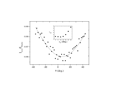
In fig.5 is reported the intensity of the transition B, normalized to the related elastic peak intensity, as a function of the polar angle, expression 4 is a trial function with the scaling factor R used as a free parameter. The fitting procedure has been repeated for several value of ranging from zero to 90∘. In the insert of fig.5 is reported the as a function of from which it is possible to conclude that the proposed model can be accepted for values of in the range 0-15∘ where the is almost constant and equal to 1. From the structural point of view this correspond to have the plane of the molecule oriented almost perpendicular to the surface plane. The best R value is 0.54 that suggests an almost equal probability for L+D and D+L scattering channels. This finding is in agreement with previous similar experiments on clean surfaces Ruocco et al. (1999a) that support the hypothesis of incoherent superposition of the two, equally relevant, scattering channels contributing to the EEL spectrum. Once more, momentum resolved EELS from adsorbed molecules has been shown to be a sensitive, accurate tool for determining orientation with respect to the substrate surface of thin molecular films.
IV Conclusions
In conclusion, the early stage of absorption of CuPc on the Al(100) surface has been studied by angle resolved EELS. The method has proven to be very sensitive and it allows to investigate coverages as low as 1 Å. The first monolayer of molecules suffers a massive charge transfer from the substrate inhibiting the optical B and Q absorption bands that are instead characteristic of bulk aggregation. This finding suggests that CuPc interacts with the Al substrate via a strong ionic bond. The molecule substrate interaction is also testified by the observed shift in frequency of the Al surface plasmon. For the thick overgrown film the molecular plane is oriented predominantly perpendicular to the substrate plane and, in contrast to the first adsorbed layer, it does not show evidences for charge transfer from the substrate (B and Q band are restored).
References
- Leznoff and Lever (1989) C. C. Leznoff and A. B. P. Lever, Phthalocyanines, Vol. 1 (VCH Publ., New York, 1989).
- Lucia and Verderame (1968) E. A. Lucia and F. D. Verderame, Journal of Chemical Physics 48, 2674 (1968).
- Canadell and Alvarez (1984) E. Canadell and S. Alvarez, Inorganic Chemistry 23, 573 (1984).
- Dogo et al. (1992a) S. Dogo, J. Germain, C. Maleysson, and A. Pauly, Thin Solid Films 219, 251 (1992a).
- Dogo et al. (1992b) S. Dogo, J. Germain, C. Maleysson, and A. Pauly, Thin Solid Films 219, 244 (1992b).
- Tokito et al. (1994) S. Tokito, J. Sakata, and Y. Taga, Applied Physics Letters 64, 1353 (1994).
- Smolyaninov (1996) I. Smolyaninov, Surface Science 364, 79 (1996).
- Dufour et al. (1994) G. Dufour, C. Poncey, F. Rochet, H. Roulet, M. Sacchi, M. De Santis, and M. De Crescenzi, Surface Science 319, 251 (1994).
- Walzer and Hietschold (2001) K. Walzer and M. Hietschold, Surface Science 471, 1 (2001).
- Dufour et al. (1995) G. Dufour, C. Poncey, F. Rochet, H. Roulet, S. Iacobucci, M. Sacchi, F. Yubero, N. Motta, M. Piancastelli, A. Sgarlata, et al., Journal of Electron Spectroscopy and Related Phenomena 76, 219 (1995).
- Cox et al. (1999a) J. Cox, S. Bayliss, and T. Jones, Surface Science 433, 152 (1999a).
- Cox et al. (1999b) J. Cox, S. Bayliss, and T. Jones, Surface Science 425, 326 (1999b).
- Ottaviano et al. (1997) L. Ottaviano, S. Di Nardo, L. Lozzi, M. Passacantando, P. Picozzi, and S. Santucci, Surface Science 373, 318 (1997).
- Shimada et al. (1998) T. Shimada, K. Hamaguchi, A. Koma, and F. S. Ohuchi, Applied Physics Letters 72, 1869 (1998).
- Koma (1992) A. Koma, Surface Science 267, 29 (1992).
- Tada et al. (1992) H. Tada, K. Saiki, and A. Koma, Surface Science 268, 387 (1992).
- Leznoff and Lever (1996) C. C. Leznoff and A. B. P. Lever, Phthalocyanines, Vol. 4 (VCH Publ., New York, 1996).
- Poirier and Pylant (1996) G. Poirier and E. Pylant, Science 272, 1145 (1996).
- Bohringer et al. (1997) M. Bohringer, R. Berndt, and W.-D. Schneider, Physical Review B (Condensed Matter) 55, 1384 (1997).
- Evangelista et al. (submitted) F. Evangelista, A. Ruocco, V. Corradini, C. Mariani, and M. G. Betti, Surface Science (submitted).
- Yokoyama et al. (2001) T. Yokoyama, S. Yokoyama, T. Kamikado, Y. Okuno, and S. Mashiko, Nature 413, 619 (2001).
- Joachim et al. (2000) C. Joachim, J. Gimzewski, and A. Aviram, Nature 408, 541 (2000).
- Scrocco et al. (1993) M. Scrocco, C. Ercolani, and A. Paoletti, Journal of Electron Spectroscopy and Related Phenomena 63, 155 (1993).
- Tada et al. (1989) H. Tada, K. Saiki, and A. Koma, Japanese Journal of Applied Physics, Part 2 (Letters) 28, L877 (1989).
- Bubnov and Frankevich (1974) L. Bubnov and E. Frankevich, Sovietic Physics Solid State 16, 994 (1974).
- Schechtman and Spicer (1970) B. Schechtman and W. Spicer, Journal of Molecular Spectroscopy 33, 28 (1970).
- Tyliszczak et al. (1989) T. Tyliszczak, F. Esposto, and A. Hitchcock, Phys. Rev. Lett. 62, 2551 (1989).
- Ruocco et al. (1999a) A. Ruocco, M. Milani, S. Nannarone, and G. Stefani, Phys. Rev. B 59, 13359 (1999a).
- Verucchi and Nannarone (2000) R. Verucchi and S. Nannarone, Review of Scientific Instruments 71, 3444 (2000).
- Donzello (2000) M. Donzello, Ph.D. thesis, Università La Sapienza, Roma (2000).
- Musket et al. (1982) R. Musket, W. McLean, C. Colmenares, D. Makowiecki, and W. Siekhaus, Applications of Surface Science 10, 143 (1982).
- Raether (1980) H. Raether, Excitation of plasmons and interband transitions by electrons (Springer-Verlag, Berlin, 1980).
- Hoffman et al. (1988) A. Hoffman, T. Maniv, and M. Folman, Surface Science 193, 513 (1988).
- Kloos (1968) T. Kloos, Z. Phys. 208, 77 (1968).
- Ruocco et al. (1999b) A. Ruocco, M. Milani, S. Nannarone, and G. Stefani, Journal De Physique. IV : JP 9, Pr6 (1999b).
- Saldin (1988) D. K. Saldin, Physics Review Letters 60, 1197 (1988).
- Schaffer and Gouterman (1972) A. Schaffer and M. Gouterman, Theoretica Chimica Acta 25, 62 (1972).
- Schaffer et al. (1973) A. Schaffer, M. Gouterman, and E. Davidson, Theoretica Chimica Acta 30, 9 (1973).
- Gouterman (1978) M. Gouterman, The Porphyrins, Vol. III, Part A (Academic Press, New York, 1978).
- Hebard (1994) A. Hebard, Physica B: Condensed Matter 197, 544 (1994).
- Hill and Kahn (1998) I. G. Hill and A. Kahn, Journal of Applied Physics 84, 5583 (1998).
- Hill and Kahn (1999) I. G. Hill and A. Kahn, Journal of Applied Physics 86, 2116 (1999).
- Maxwell et al. (1994) A. J. Maxwell, P. A. Bruhwiler, A. Nilsson, N. Martensson, and P. Rudolf, Physical Review B 49, 10717 (1994).