AFM local oxidation nanopatterning of a high mobility shallow 2D hole gas.
Abstract
Recently developed AFM local anodic oxidation (LAO) technique offers a convenient way of patterning nanodevices, but imposes even more stringent requirements on the underlying quantum well structure. We developed a new very shallow quantum well design which allows the depth and density of the 2D gas to be independently controlled during the growth. A high mobility ( cm2/Vs at 4.2 K) 2D hole gas just 350 Å below the surface is demonstrated. A quantum point contact, fabricated by AFM LAO nanopatterning from this wafer, shows 9 quantum steps at 50 mK.
Rapidly developing area of physics of nanodevices laid down new demands to heterostructure design, for example, shallow 2D gas is required in order to improve size control and enhance the confining potential. Even more stringent requirements are imposed by recently developed AFM local anodic oxidation nanolithography (LAO), which promise a low-energy high resolution alternative to the conventional e-beam lithographysc ; held97 ; bo02 . A key to the success of LAO is the properly designed heterostructure. The maximum depth of the LAO grown oxide is 100-150 Å, and shifting the surface by this amount should effectively deplete the underlying 2D gas. Experimentally it has been deduced that 2D gas should be Å below the surfaceheld98 . In conventionally grown shallow modulation doped quantum wells (QWs) -doping provides carriers to the 2D gas and compensates the surface potential of GaAs. There is a delicate balance between underdoping, when most of the carriers are trapped at the surface and no carriers left to form the 2D gas, and overdoping, when -doping layer becomes conducting at low temperatures. An addition of another doping layer at the other side of the QW reduces the necessary amount of the dopants in the top layer, but precise control of the final density of the 2D gas is still difficult.
We developed a novel heterostructure design which does not suffer from either of the above mentioned drawbacks. The as-grown structure of a shallow p-type QW consists of a GaAs buffer grown on a [11] substrate, followed by 3000 Å AlGaAs (x=0.32), Si -doping ( cm-2), 500 Å AlGaAs setback, 150 Å GaAs QW, 100 Å AlGaAs barrier, 100 Å GaAs, Si -doping ( cm-2), and 150 Å GaAs cap layer. The calculated band diagram of this structure is plotted in Fig. 1 sim ; tan90 ; snider90 . The top -doping resides in GaAs and serves the purpose of compensating the surface potential and pinning the valence band edge at the Fermi energy . The doping should be low enough to avoid conduction through this layer at low temperatures. The design relaxes the criticality of the exact amount of doping because this doping layer does not provide carriers to the underlying 2D gas. The carriers are supplied by the bottom -doping. Again, the design provides some window for the doping concentration because the density of the 2D gas is determined by the setback thickness. An excessive doping leads to the outdiffusion of dopants toward the QW and degradation of the mobilitypfeiffer91 . Indeed, we have grown two wafers with 3 times different concentration of the bottom doping; both QWs have hole concentrations different by %, but the wafer with lower doping has 8 time higher mobility.
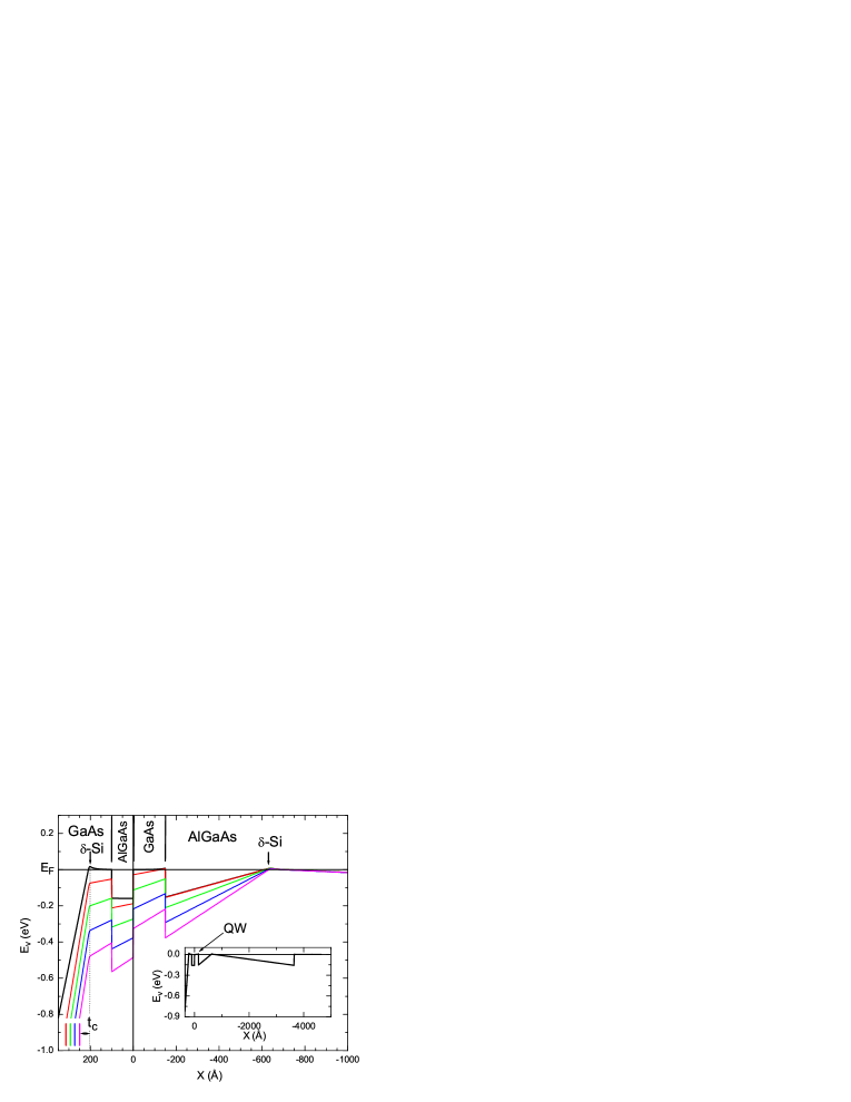
The band diagram is very sensitive to the thickness of the GaAs cap layer and, thus, is ideal for the LAO nanolithography. In Fig. 1 we simulated the effect of the LAO by reducing the by the oxide thickness. The 2D hole gas is depleted when Å, which corresponds to the oxide thickness of 60 Å. 100 Å of the oxide is estimated to lower the in the QW region by 200 meV below the , creating the corresponding barrier for the adjacent 2D hole gas.
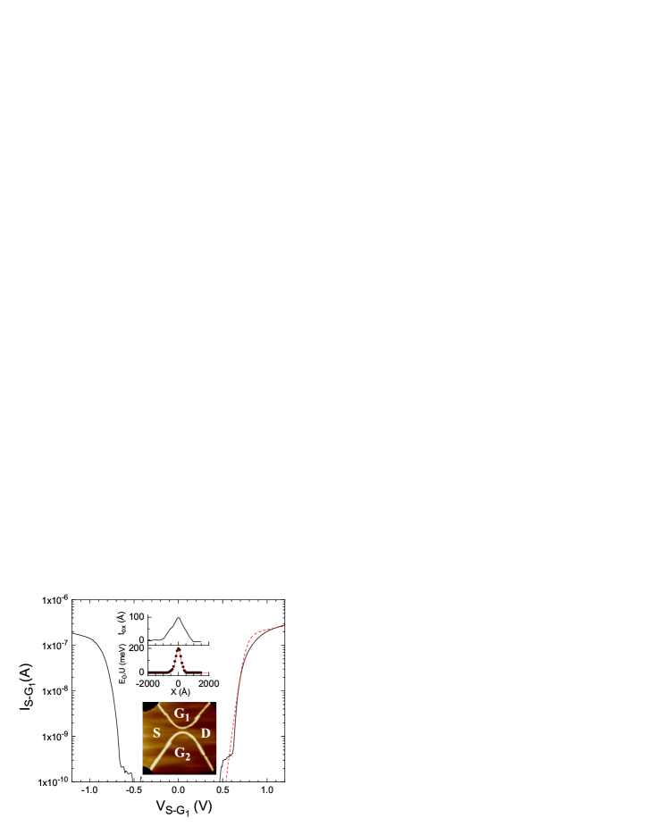
We have grown a wafer using the above parameters. The wafer has the hole density cm-2 and mobility cm-2/Vs at 0.3 K, the highest reported for so shallow (350 Å below the surface) a 2D hole gas. An AFM image of a quantum point contact, fabricated from this wafer using AFM LAO, is shown in the inset in Fig. 2. Profile of the oxide is plotted in the top inset. Position of the first energy level in the QW, relative to the level position far from the oxide line, is extracted from the band calculations and plotted with black dots. Due to non-monotonic dependence of the on the oxide thickness, width of the potential barrier is narrower by factor of 2 than the thickness of the oxide line and is Å at half height. The current–voltage (IV) characteristic across the oxide line, measured at 4.2 K, is shown in Fig. 2. Current is negligible at V and there is a sharp turn on of the current at V. We model the IV characteristic by calculating the tunneling probability through the barrier
where is the height of the potential under the center of the oxide line, is the applied voltage, and is related to the width of the oxide line. This potentialllqm provides a good approximation to the expected potential, see solid line in the inset in Fig. 2. The turn on voltage is not very sensitive to at low temperatures for our barrier widths, as well as to the exact shape of the potential. The calculated current is plotted in Fig. 2 with the dashed line. The turn on voltage for meV is close to the experimentally measure one. This value of is consistent with the estimate of the tunneling barrier for 100 Å oxidation from band calculations. Experimentally, IV characteristic is linear for oxidations depth Å, indicating that no tunneling barrier is formed, also consistent with the band calculations.
Finally, we present transport characteristics of the point contact. In Fig. 3 differential conductance is plotted as a function of the gate voltage at 50 mK. The is quantized in units of , and up to 9 plateaus can be clearly seen. Large number of steps indicate low disorder in the vicinity of the point contact. Thus, the designed heterostructure, in combination with LAO technique, provides an easy and reliable method of fabricating high quality nanostructures with sub-nanometer control over the size, shape and position.
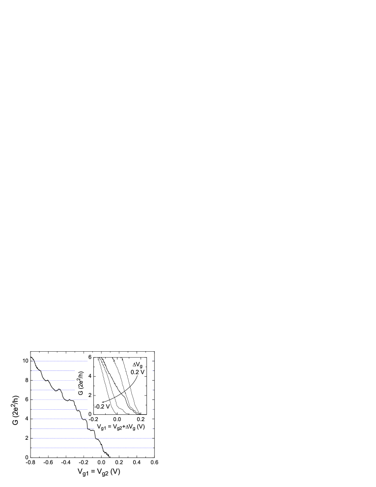
Previously, it has been shown that the position of the change can be shifted by applying a voltage difference between the gatesheinzel00 . Moreover, the barrier width under the oxide and, correspondingly, the electrostatic coupling, can be also adjusted. The effect is the best demonstrated at elevated temperatures, when steps are smeared out and the slope reflects the electrostatic coupling between the gates and the 1D channel. In the inset in Fig. 3 is plotted as a function of for different values of at 4 K . The slope increases with the increase of , indicating large electrostatic coupling between one of the gates and the channel. This enhancement is due to non-liner dependence of both channel and barrier widths on the gate voltage for in-plane gateslarkin90 .
To summarize, we developed a novel heterostructure design for reliable and reproducible growth of high mobility shallow QWs. We demonstrate the design by fabricating a high quality quantum point contact from such a wafer using AFM local anodic oxidation technique. We show that amplitude of potential barriers, formed by local oxidation of the surface, can be reliably predicted using readily available numerical simulation tools.
We thank E.V. Tsiper for discussions. The work was supported by a DURINT grant through the ONR and MARCO Focused Research Center on Meterials, Structures, and Devices which is funded at the MIT, in part by MARCO under contract 2001-MT-887 and DARPA under grant MDA972-01-1-0035.
References
- (1) E. S. Snow and P. M. Campbell, Appl. Phys. Lett. 64, 1932 (1994); E. S. Snow and P. M. Campbell, Science 270, 1639 (1995).
- (2) X.-Z. Bo et al., Mat. Res. Soc. Symp. Proc. 686, A6.5.1 (2002).
- (3) R. Held et al., Appl. Phys. Lett. 71, 2689 (1997).
- (4) R. Held et al., Appl. Phys. Lett. 73, 262 (1998).
- (5) Calculations were performed using G. L. Snider’s 1D Poisson solver.
- (6) G. L. Snider, I.-H. Tan, and E. L. Hu, J. Appl. Phys. 68, 2849 (1990).
- (7) I.-H. Tan, G. L. Snider, L. D. Chang, and E. L. Hu, J. Appl. Phys. 68, 4071 (1990).
- (8) L. Pfeiffer, E. F. Schubert, K. W. West, and C. W. Magee, Appl. Phys. Lett. 58, 2258 (1991).
- (9) Schrodinger equation for this potential can be solved analitically, see L. D. Landau and E. M. Lifshitz, Quantum Mechanics : Non-Relativistic Theory (Pergamon Press, Oxford, 1991).
- (10) T. Heinzel et al., Phys. Rev. B 61, R13353 (2000).
- (11) I. A. Larkin and V. B. Shikin, Phys. Lett. A 151, 335 (1990).