Spin-dependent tunnelling through a symmetric barrier
Abstract
The problem of electron tunnelling through a symmetric semiconductor barrier based on zinc-blende-structure material is studied. The Dresselhaus terms in the effective Hamiltonian of bulk semiconductor of the barrier are shown to result in a dependence of the tunnelling transmission on the spin orientation. The difference of the transmission probabilities for opposite spin orientations can achieve several percents for the reasonable width of the barriers.
pacs:
72.23.-b, 73.63.-bLately spin polarized electron transport in semiconductors attracts a great attention. spintronic One of the major problems of general interest is a possibility and methods of spin injection into semiconductors. A natural way to achieve spin orientation in experiment is the injection of spin polarized carriers from magnetic materials. Although significant progress has been made recently, Zhu ; Hammar ; Hanbicki ; Safarov reliable spin-injection into low-dimensional electrons systems is still a challenge. Schmidt et al. pointed out that a fundamental obstacle for electrical injection from ferromagnetic into semiconductor was the conductivity mismatch of the metal and the semiconductor structure. Schmidt However, Rashba showed that this problem could be resolved by using tunnelling contact at the metal-semiconductor interface. Rashba2 On the other hand Voskoboynikov et al. Vosk1 proposed that asymmetric non-magnetic semiconductor barrier itself could serve as a spin filter. It was demonstrated that spin-dependent electron reflection by inequivalent interfaces resulted in the dependence of the tunnelling transmission probability on the orientation of electron spin. This effect is caused by interface-induced Rashba spin-orbit coupling Rashba and can be substantial for resonant tunnelling through asymmetric double-barrier Vosk2 ; Silva or triple-barrier Koga heterostructures. However, in the case of symmetric potential barriers, the interface spin-orbit coupling does not lead to a dependence of tunnelling on the spin orientation.
In this communication we will show that the process of tunnelling is spin dependent itself. We demonstrate that a considerable spin polarization can be expected at tunnelling of electrons even through a single symmetric barrier if only the barrier material lacks a center of inversion like zinc-blende structure semiconductors. The microscopic origin of the effect is the Dresselhaus terms Dresselhaus in the effective Hamiltonian of the bulk semiconductor of the barrier.
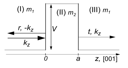
We consider the transmission of electrons with the initial wave vector through a flat potential barrier of height grown along direction (see Fig. 1); is the wave vector in the plane of the barrier, and is the wave vector normal to the barrier pointing in the direction of tunnelling. The electron Hamiltonian of the barrier in effective mass approximation contains the spin-dependent term (Dresselhaus term) Dresselhaus
| (1) |
where are the Pauli matrices, is a material constant (see Table 1), and the coordinate axis are assumed to be parallel to the cubic crystallographic axis , , , respectively. In the case of tunnelling along one should consider in the Hamiltonian as an operator . We assume the kinetic energy of electrons to be substantial smaller than the barrier high , then the Hamiltonian (1) is simplified to
| (2) |
One can note that essentially induces a
spin-dependent correction to the effective electron mass
along in the
barrier.
| GaSb | InAs | GaAs | InP | InSb | |
| , eVÅ3 | 187 | 130 | 24 | 8 | 220 |
| 0.041 | 0.023 | 0.067 | 0.081 | 0.013 |
Table 1: Parameters of band structure of various A3B5 semiconductors. PT ; IP
The Hamiltonian (2) is diagonalized by spinors
| (3) |
which correspond to the electron states ”” and ”” of the opposite spin directions. Here is the polar angle of the wave vector in the plane , being
| (4) |
Transmission probabilities for the electrons of eigen spin states ”” and ”” (3) are different due to spin-orbit term (2). The orientations of spins in the states ”” and ”” depend on the in-plane wave vector of electrons and are given by
| (5) |
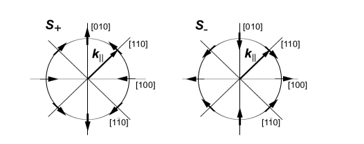
Fig. 2 demonstrates the orientations of spins and for various directions of the in-plane electron wave vector , i.e. as a function of polar angle . If is directed along a cubic crystal axis ( or ) then the spins are parallel (or antiparallel) to , while are perpendicular to if the in-plane wave vector is directed along the axis or .
Electrons of the eigen spin states ”” and ”” propagate through the barrier with conserving of the spin orientation. Since the wave vector in the plane of the barrier is fixed, wave functions of the electrons can be written in the form
| (6) |
where is a coordinate in the plane of the barrier. The function in the regions I (incoming and reflected waves, see Fig. 1), II and III (transmitted wave) has the form
| (7) |
respectively. Here and are the transmission and reflection coefficients for spin states , respectively, and the wave vectors under the barrier are given by
| (8) |
where is the reciprocal length of decay of the wave function in the barrier for the case when the spin-orbit interaction (1) is neglected
| (9) |
and () are the effective masses outside and inside the tunnelling barrier, respectively. Taking into account the boundary conditions, which require that
| (10) |
are continuous at the interfaces, a system of linear equations for , , , and can be derived. Solution of the system allows one to calculate the coefficients of the transmission . For the real case they are derived to be
| (11) |
where is the transmission coefficient when the spin-orbit interaction (1) is neglected,
| (12) |
is the width of the barrier. The general problem of tunnelling of an electron with arbitrary initial spinor can be solved by expanding to the eigen spinors .
It is convenient to introduce a polarization efficiency that determines the difference of tunnelling transmission probabilities for the spin states ”” and ”” through the barrier
| (13) |
In our case it has the form
| (14) |
At a given initial wave vector of electrons, , the polarization efficiency drastically increases with the strength of the Dresselhaus spin-orbit coupling (see Eq. 14), and the barrier width . However while increase the barrier width increases the tunnelling efficiency one should keep in mind that the barrier transparency decreases simultaneously (see Eq. (12)). In Fig. 3 the efficiency and the barrier transparency are plotted as a function of the barrier width, , for various barrier materials.
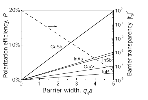
The material parameters and effective mass used in the calculations are given in the Table 1. One can see that for a reasonable set of parameters given in the figure caption it is possible to achieve spin polarizations of several percents. Tunnelling barriers prepared on the basis of GaSb or its solutions seem to be the most efficient barrier materials for spin selective tunnelling because of the large value of the product .
The polarization strongly depends on the electron wave vector parallel to the barrier (see Eq. (14)). This result suggests a device for spin injection into quantum wells. Let’s assume two quantum wells separated by a tunneling barrier, and a current flowing along one of the quantum wells. The in-plane current results in non-zero average electron wave vector and, due to the considered effect, in a spin polarization of carriers.
In conclusion, we have demonstrated that the Dresselhaus terms in the effective Hamiltonian of semiconductors lacking a center of inversion yield a considerable spin polarization of electrons tunnelling through barriers. The effect could be employed for creating spin filters, eg. on the base of type-II strained heterostructures like InAs/GaSb, InSb/GaSb and GaSb/GaAs.
The work was supported by the RFBR, the Presidium of the RAS, and grants of the DFG and INTAS.
References
- (1) Semiconductor Spintronics and Quantum Computation, eds. D.D. Awschalom, D. Loss, and N. Samarth, in the serie Nanoscience and technology, eds. K. von Klitzing, H. Sakaki, and R. Wiesendanger (Springer, Berlin, 2002).
- (2) H.J. Zhu, M. Ramsteiner, H. Kostial, M. Wassermeier, H.-P. Schönherr, and K.H. Ploog, Phys. Rev. Lett. 87, 016601 (2001).
- (3) P.R. Hammar, and M. Johnson, Appl. Phys. Lett. 79, 2591 (2001).
- (4) A.T. Hanbicki, B.T. Jonker, G. Itskos, G. Kioseoglou, and A. Petrou, Appl. Phys. Lett. 80, 1240 (2002).
- (5) V.F. Mostnyi, V.I. Safarov, J. De Boeck, J. Das, W. van Roy, E. Goovaerts, and G. Borghs, cond-mat/0110240
- (6) G. Smidt, D. Ferrand, L.W. Molenkamp, A.T. Filip, and J. van Wees, Phys. Rev. B62, R4790 (2000).
- (7) E.I. Rashba, Phys. Rev. B62, R16267 (2000).
- (8) A. Voskoboynikov, S.S. Liu, and C.P. Lee, Phys. Rev. B58, 15397 (1998).
- (9) Yu.A. Bychkov and É.I. Rashba, Pis’ma Zh. Eksp. Teor. Fiz. 39, 66 (1984) [JETP Lett. 39, 78 (1984)].
- (10) A. Voskoboynikov, S.S. Liu, and C.P. Lee, Phys. Rev. B59, 12514 (1999).
- (11) E.A. de Andrada e Silva, G.C. La Rocca, Phys. Rev. B59, 15583 (1999).
- (12) T. Koga, J. Nitta, H. Takayanagi, and S. Datta, Phys. Rev. Lett. 88, 126601 (2002).
- (13) G. Dresselhaus, Phys. Rev. 100, 580 (1955).
- (14) G.E. Pikus, A.N. Titkov, in Optical Orientation, eds. F. Meier and B.P. Zakharchenya (Elsevier, Amsterdam, 1984).
- (15) E.L. Ivchenko and G.E. Pikus, Superlattices and Other Heterostructures. Symmetry and Optical Phenomena (Springer, Berlin, 1995), [2nd edition 1997].