[
Evolution of a Metal to Insulator Transition in Ca2-xNaxCuO2Cl2, as seen by ARPES
Abstract
We present angle resolved photoemission (ARPES) data on Na-doped Ca2CuO2Cl2. We demonstrate that the chemical potential shifts upon doping the system across the insulator to metal transition. The resulting low energy spectra reveal a gap structure which appears to deviate from the canonical d form. To reconcile the measured gap structure with d-wave superconductivity one can understand the data in terms of two gaps, a very small one contributing to the nodal region and a very large one dominating the anti-nodal region. The latter is a result of the electronic structure observed in the undoped antiferromagnetic insulator. Furthermore, the low energy electronic structure of the metallic sample contains a two component structure in the nodal direction, and a change in velocity of the dispersion in the nodal direction at roughly 50 meV. We discuss these results in connection with photoemission data on other cuprate systems.
]
I Introduction
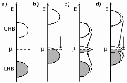
The close proximity of an antiferromagnetic Mott insulating phase suggests that this insulator may be the natural starting point for understanding the unusually high superconducting transition temperatures as well as the unconventional normal state properties[5] in the cuprates. The insulator to metal transition in strongly correlated materials is a well studied fundamental problem in solid state physics in its own right. Even by limiting ourselves to a one band Hubbard model, which may be an appropriate starting point for the half-filled cuprates,[6] there remain several ways one could imagine the electronic structure evolving upon doping (see figure 1). One scenario is the chemical potential shifting to the top of the valence band similar to the case of a band insulator.[7] An alternative scenario is states being created inside the Mott gap upon doping.[8, 9] These are the two most commonly discussed pictures with regard to the cuprates.
ARPES studies of the La2-xSrxCuO4 (LSCO) system show that spectral weight is transfered to low energy states, which lie inside the Mott gap, upon hole doping.[8, 9, 10, 11] In contrast, in the Bi2Sr2Ca1-xYxCu2O8+δ (Bi2212) and Nd2-xCexCuO4 (NCCO) systems there is work which shows that the chemical potential shifts in addition to a transfer of spectral weight.[12, 13] A potential problem for the Bi2212 system is the difficulty to obtain deeply underdoped samples. The oxychlorides, Sr2CuO2Cl2 and Ca2CuO2Cl2, are single layer cuprates that have provided the best photoemission data on the undoped insulating state to date. Thus the oxyhalides are ideal systems to study the metal to insulator transition with photoemission, as high quality single crystals, which cleave as easily as the Bi2212 system, can now be grown through the metal to insulator transition.
Recently, we have reported that the chemical potential shifts upon doping the insulator, Ca2CuO2Cl2(CCOC), with Na.[14] Here we present the full body of evidence which supports arguments for such a shift of the chemical potential in the Ca2-xNaxCuO2Cl2 system. We examine the valence band and photon energy dependence of Na-doped CCOC and compare it with that found in the insulator. By making a detailed comparison of the low energy spectra we unambiguously show that the high energy pseudogap is in fact a result of the d-wave-like dispersion seen in the insulator, as had been suggested previously.[15, 16]
As we will show, residual effects from the insulator strongly distort the ”band structure” in these deeply underdoped samples resulting in a gap structure along the LDA-predicted Fermi surface that strongly deviates from the canonical d form. In order to reconcile this result with d-wave superconductivity, we conclude that the measured gap structure is a consequence of probing two different regimes. One regime is concerned with a small unresolved gap along a hole pocket about . The second regime is in the vicinity of where a large gap, which we identify as the pseudogap, is identified with the undoped insulator. This picture is consistent with the observed chemical potential shift.
The evolution of the electronic structure, however, is not solely a simple shift of the chemical potential since the spectral lineshape also evolves with doping. We further investigate here the two component structure found in the nodal direction of Ca2-xNaxCuO2Cl2.[14] We show that this structure is not directly related to Tc, and from a MDC (Momentum Distribution Curve) analysis we find a “kink” in the dispersion which has the same energy as the ”dip” which divides the two components in the EDCs (Energy Distribution Curves). The observation of a kink near 50 meV in this system supports the observed universality of this type of behaviour in the cuprates.[17] Finally, we discuss the similarities and differences between photoemission results from other cuprates and Na-doped CCOC.
II Experimental
Na-doped CCOC single crystals were grown by a flux method under high pressure, by using a cubic anvil type pressure apparatus.[18] A powder mixture of Ca2CuO2Cl2, NaCl, NaClO4, and CuO (1:0.2:0.2:0.1 molar ratio), sealed in a gold tube, was heated to 1250∘C and then slowly cooled to 1050∘C under high pressure. Uniform samples at various Na concentrations, x, were achieved by using different pressures during the synthesis. 4 GPa and 5 GPa gave a Na concentration of 10 and 12, respectively. Crystals with a maximum dimension of 1.5 1.5 0.1 mm3 were obtained. The Na content was estimated by comparing the c-axis lattice constant with powdered ceramic samples of known content.[19] Magnetization measurements of Tc gave results consistent with the assigned doping concentrations. The Na concentrations used in this study were x=0.10(Tc=13) and x=0.12(Tc=22 K). Since superconductivity does not occur until x0.08 in the Na-doped CCOC system,[18, 19] we consider our samples to lie in the heavily underdoped regime. As a reference, the optimal Tc in powder samples has been found to be 28 K.[19] ARPES measurements were performed on beamline 5-4 of SSRL. The samples were easily cleaved in situ and measured at the indicated temperatures in the figure captions. The angular resolution was 0.29∘, while the energy resolution was always 30 meV. When examining the detailed low energy excitations (ie after figure 7) the energy resolution was improved to 15 meV.
III Data and Results
A Valence Band
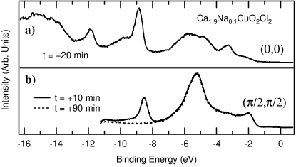
We begin with the valence band spectra of Na-doped CCOC in figure 2, which illustrates a peculiarity of this system. Namely, from 8 to 13 eV binding energy there exists several pronounced features which rapidly vanish with time. The spectra from the cleave where these features were most prominent is shown in the top panel. Features are visible at 9, 10, and 12 eV which are not observed in the parent compound, CCOC. Figure 2b reveals that within 90 minutes following the initial cleave, the additional features from 8 to 11 eV have vanished. The feature at 12 eV also vanishes (not shown). For binding energies less than 7 eV no change in the spectra was observed over these time scales where particularly close attention was paid to the near features, less than 1 eV binding energy. The photon energy was adjusted to ensure the high binding energy features were not derived from a contribution of second order light from the monochromator. Comparing the spectra in panels a) and b) suggests a dispersive nature of the additional peaks not seen in the insulating compound. However, it was also observed that these features shift to lower binding energy as they age. We tentatively assign the origin of these features from 8 to 13 eV binding energy to flux inclusions, such as NaCl and NaClO4 which are used in excess during the synthesis;[20] subsequently the surface of these flux inclusions are passivated by the photon following the cleave. Despite the uncertain nature of these high energy features, the fact that the low binding energy region of the spectra have no variation over the short time scale in which the high energy features vanish, gives us confidence that our low energy results on the Na-doped CCOC crystals are intrinsic.
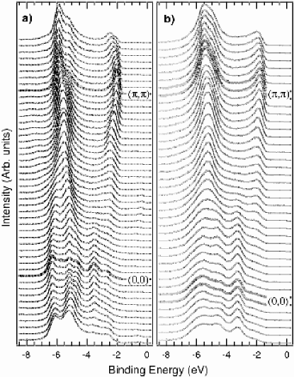
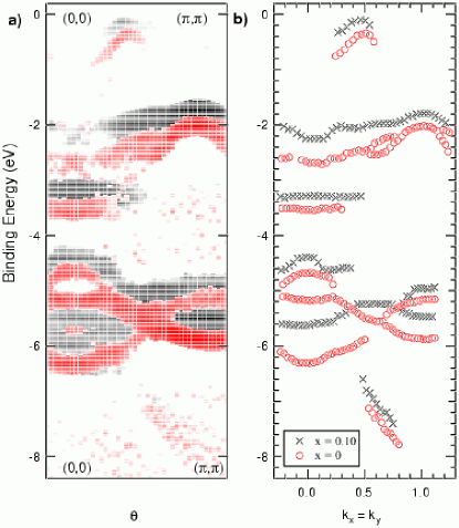
Figure 3 compares the valence band spectra along the nodal direction for x=0 and x=0.1. The data on the insulator are consistent with previous reports on a similar material (Sr2CuO2Cl2),[21, 22] and the data for the Na-doped Ca2CuO2Cl2 were reproduced on multiple cleaves. The position of the valence band in the insulator with respect to the chemical potential can vary as much as 1 eV which is believed to be a result of pinning the chemical potential at different impurity levels that exist for the different cleaved surfaces. It is important to note that the valence band data of the insulator shown in figures 3 and 4 are at the minimum possible binding energy, since if they are shifted further towards the chemical potential, spectral weight from the tail of the valence band peaks would be pushed above the chemical potential falsely indicative of a metallic nature. The low energy excitations within 1 eV of the chemical potential, which the remainder of this paper will focus on, are barely visible on this broad scale. Generally, the two data sets are quite similar, although differing relative intensities for a few of the bands about (0,0) can be seen. The other difference is that the insulator data are sharper than those of the metal. Perhaps this is an indication that the surface of Na-doped Ca2CuO2Cl2 is not as well ordered as the pure sample grown under atmospheric conditions. Figure 4a plots the second derivative of the above spectra, which can be used to more clearly identify the dispersion of various features. This method agrees with the dispersion extracted by the peak positions of the various bands in the insulator and the metal as shown in panel 4b. The resolved bands appear to have shifted to lower binding energy with doping by roughly 300 meV, as would be expected if this were a simple band material. One apparent exception exists from the band at 5.6 eV binding energy in the metallic sample near (0,0) in figure 4b. However, due to the broadness of the features in the metal, it is likely that this band is a superposition of several peaks, resulting in this apparent discrepancy. Note that in the insulator several bands are resolved in this same region. Thus, the overall picture from the valence band data is highly suggestive of a chemical potential shift with doping. The most convincing demonstration for this is at where the peaks for both concentrations are most clearly resolved. Here, the peak positions indicate that the insulator is shifted to higher energy by at least 300 meV relative to the metal. The specific value will depend on which insulating data set is used, since the chemical potential in the insulator can vary substantially as mentioned above. We again emphasize that the current binding energy of the insulator could not be found at smaller binding energies without spectral weight being shifted unrealistically above the chemical potential. Thus, neither charging of the insulator nor the variability of the chemical potential in the insulator can be responsible for the observed shift upon doping
B Near EF Comparison
To further support this idea, figure 5 presents spectra near EF along the entire (0,0) to and (0,0) to lines, where all the spectra from this insulating data set have been shifted by 750 meV so that the centroid of the feature at is at the chemical potential. The value of 750 meV is specific to this particular data set, but is 300 meV more than allowed by the uncertainty in the position of the chemical potential. Along (0,0) to the spectra are remarkably similar. In many instances fine details of the line shape match extremely well. For example, a second broad component in the electronic structure can be observed at roughly 600 meV higher binding energy from the first feature creating a heavily asymmetric lineshape.[23, 24] This indicates that upon doping the chemical potential simply drops to intersect the top of the valence band similar to the case of an ordinary band material. This would naturally explain the large high energy pseudogap seen at as a remnant property of the insulator as first suggested by Laughlin.[15, 16]
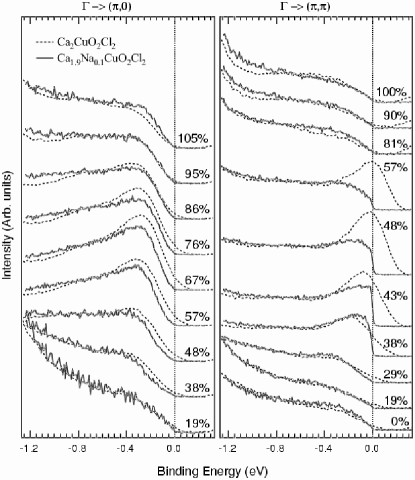
Along (0,0) to the situation is less clear. As the feature moves towards lower binding energy a sharp Fermi cutoff appears in the metallic samples, as anticipated by the large peak at the Fermi level from the energetically shifted spectra of the insulating sample. However, the match between the spectra becomes increasingly worse as is approached. Perhaps this simply indicates that a Fermi crossing has occurred before , and thus the weight at is suppressed relative to the insulator or that some spectral weight transfer in addition to the shift of the chemical potential has occured. To see if the suppression was due to matrix element effects we also changed the polarization to maximize the nodal direction cross section, but it remained weaker. This suppression possibly indicates that increased scattering which could effectively smear out the resolution, and would have the greatest effect where the dispersion is the steepest (near ), has occured. However, this would require a nontrivial small angle scattering mechanism, which does not simply produce an angle independent background. Also, the cleavability of the Na-doped compounds is the same as the parent insulator, and laser reflections from the sample indicate flat surfaces, which argue against angle averaging as the cause for the observed suppression of weight. Typically, highly angle dependent valence band spectra as shown in figure 3 are indicative of a good surface, although the Na-doped valence band features are somewhat broader than in the case of the insulator. Pothuizen et al.[22] noted that in SCOC the lineshape of the 2 eV binding energy peak at is identical to the lineshape of the Zhang-Rice singlet at . Given such a correlation a broadened low-energy spectral lineshape at in Na-doped CCOC is perhaps expected when the valence band at 2 eV has been broadened, as observed here (see figure 3). This suggests that the small differences between the doped system and the half filled insulator may indeed result from a difference in sample surface quality.
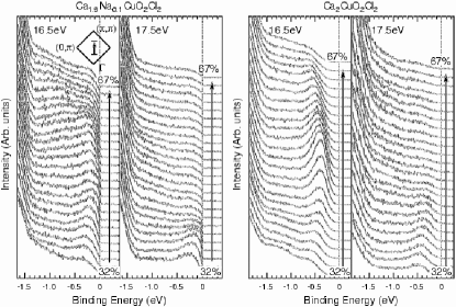
Considering that the features of hole doped CCOC track the dispersion of the features in the half filled insulator, one might wonder exactly how similar are the electronic states for the two doping levels. A good way to test this is by analyzing the photoemission matrix elements. Under the dipole approximation the photoemission intensity can be written as where are the initial and final state wavefunctions, and is the perturbing Hamiltonian.[25] Practically, this means that the cross section of the photoemission process will depend on the photon energy and experimental geometry as well as the wavefunctions themselves. Thus, if two wavefunctions are to be considered as the same, then they should have the same dependence on the experimental conditions. We have found that CCOC experiences a fairly dramatic change in the modulation of intensity along the nodal direction when changing the photon energy from 16.5 to 17.5 eV. In figure 6, we compare the EDCs along the nodal direction of a 10 Na-doped CCOC sample and an undoped CCOC sample using 16.5 eV and 17.5 eV photons. We notice that the change in the modulating intensity on going from =16.5 to 17.5 eV is similar for both samples. Namely, for 16.5 eV photons there is much more intensity at and higher values, which vanishes on going to 17.5 eV photons. Even the existence of the second feature at 600 meV higher binding energy from the lowest energy feature can be seen in both samples along the nodal direction. These results show that the gross features of the wavefunction of the electronic states within 2 eV of the chemical potential discussed thus far are remarkably similar. The peculiar photon energy dependence shown in figure 6 will be discussed separately with a much larger body of data.[26] Along with the fairly rigid shift in dispersion of the low energy states and the valence band, the lineshape comparison and photon energy dependence show conclusively that the chemical potential indeed shifts upon doping the half filled insulator, Ca2CuO2Cl2, with Na.
C Metallic Nature of Na-doped Ca2CuO2Cl2
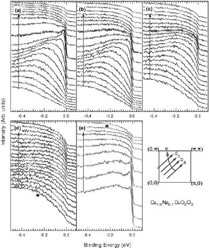
A naive expectation of a simple chemical potential shift upon doping is the creation of a small hole pocket centered at . However this contrasts with the majority of ARPES results from the optimal and overdoped regime which find a large Fermi surface centered about as predicted by band theory.[27] We shall thus take a closer look at the near EF electronic structure to see if the simple picture of a chemical potential shift as illustrated in figure 1b is correct. In other words, is the electronic structure unchanged with the exception of the position of the chemical potential? Figure 7 presents a sampling of the EDCs at selected points. The cuts shown in (a) through (d) are taken parallel to the nodal direction. For several of the cuts close to the nodal direction a broad feature starts at high binding energy and approaches the Fermi energy with increasing , where a sharp Fermi cutoff of the spectra is indicative of a Fermi surface crossing. We will return to the presence of a peak-dip-hump like structure near the nodal Fermi crossing later. The Fermi crossings, which have been determined by the spectra with the minimum leading edge midpoint (the binding energy where the spectral intensity is half of the intensity at the peak position), have been highlighted in the figure. We note that while a minimum value of the leading edge midpoint identifies the spectra which corresponds to , the value itself will be pushed back to higher binding energy if this portion of the Fermi surface is gapped. As the cuts approach the spectral features become less pronounced and it quickly becomes impossible to identify a Fermi crossing as one can no longer clearly identify a peak position to meaningfully extract a leading edge. This is best illustrated in panel (e) where spectra along the ostensible Fermi surface predicted by band theory are presented. Near the node, there is a clear Fermi cutoff at EF, but this feature disappears quickly as one approaches the antinodal region.
One can also visualize the data with an intensity map at EF, obtained by integrating each EDC by a 4 meV window about EF. The highest intensity contour, shown in figure 8a, forms what appears as a small arc.[28] The open circles indicate where a clear Fermi crossing can be observed as in the cuts shown in figure 7(a) through (c). Note this ends as the Fermi surface crosses the antiferromagnetic zone boundary. By assuming that the Fermi surface can not abruptly end in the middle of the Brillouin zone, one is left with two possibilities. Either the Fermi surface still lies along the one predicted by band theory and has been heavily gapped as one approaches or the Fermi surface is a small hole pocket centered on or near . We investigate these two possibilities below.
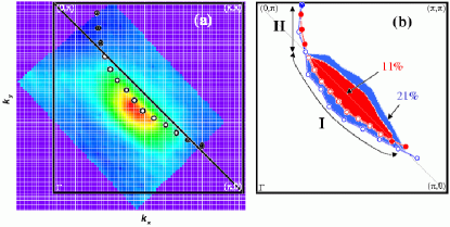
Let us first attempt to push the assumption that the large LDA-like Fermi surface holds for this heavily underdoped sample. We separate the large Fermi surface into two regions, as illustrated in figure 8b. In Region I the broad spectral function has a sharp Fermi cutoff, which clearly defines , while in region II one must extrapolate the Fermi surface from the Fermi crossings found in region I assuming a large Fermi surface that does not terminate in the middle of the Brillouin zone. This is shown by the solid dots in figure 8. Note that in the region near , variations in the precise shape of the Fermi surface will not affect the following analysis as the spectra have little variation which is apparent from the EDCs in figure 7d.
Figure 9 plots the leading edge midpoint for spectra along the large Fermi surface just discussed relative to the value at =45∘ (the nodal position for a pure d functional form). In this way one can determine the gap structure along the Fermi surface. The open symbols indicate the leading edge midpoint for the Fermi crossing spectra found in region I. However, in region II the lack of a clear leading edge midpoint prevented us from identifying a Fermi crossing in the first place. Hence, we need an alternative method to describe the dispersion. Near an energy scale (albeit a broad one) still exists in the spectra as indicated by a dot in figures 7 (d) and (e). Thus we can blindly normalize the maximum of the spectra below 300 meV to 1, and extract a leading edge midpoint via this simplified approach. This is what is shown by the filled symbols in figure 9. For a simple spectral function this procedure would give the correct gap value. In our case, one can see that close to the node this procedure roughly matches our more careful analysis, but it also allows us to extend our gap analysis beyond the regime where a clear Fermi crossing has been identified, albeit in a crude way. The solid black line is the expectation for the canonical d-wave functional form. As mentioned above, in the optimal and overdoped Bi2212 samples a simple spectral function and a large Fermi surface is observed, and the d-wave functional form well describes the experimental gap structure.[29] However, in the heavily underdoped regime studied here, there is a strong deviation from the d-wave functional form. In order to reconcile this gap structure with d-wave superconductivity[30] our assumption of a large Fermi surface centered at must break down. In this case, figure 9 is not physically significant as it maps the energy along two physically different regions as defined in figure 8b, each with its own gap structure. In other words, by assuming a d-wave gap structure we have shown that only a fraction of the spectra used for figure 9 actually lie on the Fermi surface.
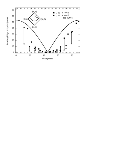
Region I does indeed represent a portion of the Fermi surface about which may contain a very small gap, while region II does not contain a Fermi crossing, and the resulting large gap identifies a larger energy scale. We have just ruled out the possibility that the Fermi surface in this sample is a large hole pocket centered at . If we maintain that the Fermi surface can not abruptly end in the middle of the Brillouin zone we must conclude that the Fermi surface forms a small hole pocket, as naively expected from the observed chemical potential shift. The question then becomes, how does such a Fermi surface develop a gap consistent with d-wave superconductivity. Given the experimental resolution we can not comment on whether or not the flat region in figure 9 would itself fit a functional form, which is the simplest expectation for d-wave pairing, although models exist with small hole pockets and d-wave pairing for which this is not the case.[32] We note that for a superconductor with a transition temperature of 13 K, the maximum of the gap from BCS theory is expected to be less than 2 meV at the antinode and even smaller along the observed arc, which is too small for our experimental resolution and is not the objective of this study. Perhaps this gap could be measured with an improved spectrometer.
By symmeterizing the hole pocket about the antiferromagnetic zone boundary one finds an area of 5.7, which implies a doping level of 11.4 due to the electron spin. This is in rough agreement with the hole doping of 10 determined by comparing Tc and lattice constants with results on powdered samples.[19] Again we note that the hole pocket is also not necessarily symmetric about the antiferromagnetic zone boundary,[32] which could substantially modify these values. The idea of a small hole pocket about in Na-doped CCOC is also consistent with the observations of shadow bands[31] at higher binding energy.[14] Presumably, the coherence factors responsible for the shadow band are very weak making it difficult to distinguish a second Fermi crossing from the background at EF. We stress that while our findings are quite consistent with the small Fermi pocket picture, we did not see the shadow Fermi surface at zero energy even though we do observe a shadow band at higher energies.
Meanwhile, the observation of a chemical potential shift in this material from the insulating state and the photon energy dependence of the lineshape emphasize that the features near (region II) in the Na-doped Ca2CuO2Cl2 sample are a direct result of the magnetism which dominates the antiferromagnetic insulator. To illustrate that the energy scale near is the same as that of the insulator, recall figure 5 where the spectra of the insulator matches that of the Na-doped sample at .
We have also repeated the above gap structure analysis on a sample with x=0.12 (Tc=22 K), and some of the results are presented in blue in figure 8 and as circles in figure 9. The data reproduce the above analysis with a few small quantitative differences. The Fermi arc increases in size (shown in figure 8b), consistent with an increase in doping, while the binding energy near reduces slightly which demonstrates that this energy scale is decreasing with increasing doping. This is also expected as we have identified this energy scale with the magnetism of the insulator whose strength should diminish together with the antiferromagnetic correlations as holes are added to the system. This has also been observed in previous studies on the high energy pseudogap.[33] We should note that the hidden message of describing the Fermi surface in the underdoped regime as a small pocket about is that the system must at some point transform upon doping to the large Fermi surface centered about observed in the overdoped regime. In measuring the volume of the pocket for the x=0.12 sample we find the doping level to be 21. The fact that this analysis begins to show a deviation from a doping level of x perhaps begins to identify a transition to a state where the doping level should be described as 1-x (the expected volume of the large Fermi surface centered at ).[34]
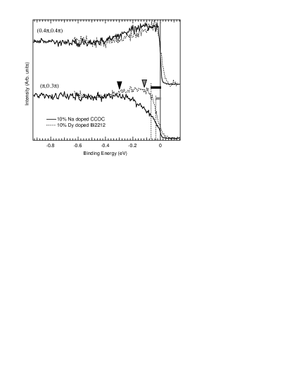
In comparison with other cuprates, the lack of a Fermi cutoff in the EDC’s would normally be identified as an extremely large pseudogap. In an attempt to quantify this suppression of weight, we compare 10 Na-doped CCOC to 10 Dy-doped Bi2212[35] in figure 10. 10 Dy-doped Bi2212 is underdoped with a Tc of 65 K giving it a Tc/Max(Tc) of 0.72, while 10 Na-doped CCOC has a ratio of 0.46. A comparison with 17.5 Dy-doped Bi2212 (not shown) with a Tc/Max(Tc) ratio of 0.28 yielded a similar comparison. One clearly observes the loss of spectral weight at the Fermi energy for the Fermi momentum of when compared to the respective Fermi crossings along the nodal direction near . There are two common methods for characterizing the pseudogap with ARPES. The first, is by the shift of the leading edge midpoint of a spectra to higher binding energy relative to the chemical potential as indicated by the dashed lines. This is typically referred to as the low energy pseudogap. For Dy-doped Bi2212 this is reasonably well defined, and gives a value of 30 meV. For the Na-doped CCOC sample, we find a value of roughly 50 meV at . However, as previously noted, the lack of a Fermi cutoff near implies that the low-energy pseudogap is not well defined in the Na-doped CCOC spectra. As a result, we are inclined to characterize the pseudogap by what is known as the high energy pseudogap which identifies a larger energy scale in the spectra about , and is sometimes referred to as a “hump”.[33] Here, we find a high energy pseudogap of roughly 300 meV for Na-doped CCOC, compared with 120 meV for Dy-doped Bi2212 as indicated by the triangles in figure 10. Independent of the method chosen, the pseudogap for Na-doped CCOC appears significantly larger than that of Bi2212 at a comparable doping level.
The high energy pseudogap seen in Bi2212 was first conjectured by Laughlin to be a result of the -wave-like modulation of the dispersion of the insulating oxy-halides.[15, 16] From the observed shift of the chemical potential it is clear that the high energy pseudogap indeed directly results from the dispersion seen in the parent compound, although it appears that the energy scales of the high energy pseudogap have a small system dependent variation. The implication for such a large pseudogap relative to the Bi2212 system at comparable doping should be investigated, and the bilayer effect in Bi2212 will need to be taken into consideration. If the condensation energy for superconductivity is acquired by the gapping of low energy states near , then this would result in superconductivity being less favorable as evidenced by the smaller optimal Tc(28 K and 90 K for Na-doped CCOC and Bi2212, respectively).
D Nodal Peak-Dip-Hump Structure
A two component structure can be seen in the low energy spectra of Na-doped CCOC at the Fermi crossing in the nodal direction. This was shown in figure 7e, where we plotted EDCs along the Fermi arc and then towards as indicated in the cartoon inset. The reason for the difference in clarity of this structure between cleaves is unknown, but is likely due to a variation of inhomogeneities and experimental conditions which make it impossible to resolve the two components that appear as one in the spectra of figure 5. Note that in general, the presence of sharp low energy features is a tribute to a high sample quality. The loss of the two component structure as one approaches is indicative of the observed large pseudogap, which precludes the identification of any similar structure in the low energy excitations near .
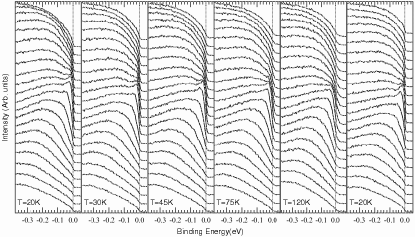
The observation of a two component structure in these superconducting samples begs the question of how it may be related to superconductivity. Figure 11 presents temperature dependence of this feature from 20 K( Tc) up to 120 K. It is clear that the peak-dip-hump like structure is observed up to 75 K, and is finally smeared out at 120 K. By cycling the temperature back down to 20 K, we ensure that the broadening at high temperatures is not an aging effect. Since even optimally doped polycrystaline samples have only a maximum Tc of 28 K, it is clear that the two component structure observed here does not turn on near Tc. This is in contrast with the more familiar two component structure in ARPES on the Bi2212 system which has now also been seen in YBCO[36] and Bi2223,[37] and does turn on with Tc.[38, 39] It is important to note that, aside from the different temperature dependence, the two component structure observed in Na-doped CCOC occurs along the nodal direction as opposed to the region as in the other cases. Furthermore, we note that CCOC is a single layer material and thus the peak-dip-hump seen here can not be a consequence of bilayer splitting as has been conjectured for the peak-dip-hump structure observed in Bi2212.[40]
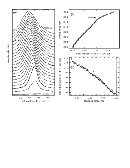
In order to gain some insight into the origin of this structure figure 12 presents a MDC analysis along the nodal direction of a x=0.10 sample. The dashed curves are the single Lorentzian fits to selected MDCs. Similar procedure in other cuprates has been used to extract self energies from the fit parameters.[17, 41, 42] Here the fits serve as a method for parameterizing the observed dispersion. Figures 12b and 12c plot the peak positions and widths as a function of the binding energy of the corresponding MDCs. A change of slope in the dispersion of the peak positions is seen near 55 meV. This value is attained from the intersection of two linear fits ranging from 0 to 30 meV and 100 to 200 meV. We shall refer to this feature as a “kink”. A similar kink in other cuprate systems has received significant attention in recent ARPES literature.[17, 42, 43, 44] Certainly, the similarity of the kink energy position to the dip energy position seen in the EDCs suggests that these two results are related. The MDC width also displays an accelerated decrease in width as indicated by the dotted lines in figure 12c.
What is the possible origin of a two component structure in the EDC near along the nodal direction? Pure macroscopic phase separation of metallic and undoped insulating domains can be ruled out, since the feature seen in the insulator would not have shifted to the chemical potential in this case. One possibility is that a sharp, coherent-like peak is growing with doping, while the incoherent features at half filling slowly vanish. This idea is captured in the recent phase string calculations done by Muthukumar, Weng, and Sheng.[45] In this sense, the two components would hint at a balance between the antiferromagnetic insulator and the drive for the system to become metallic. An alternative scenario is that the peak-dip-hump structure is the result of coupling to a collective mode. This could also naturally explain the presence of the kink. Although still a debated interpretation, Lanzara et al. propose that the universally observed kink is due to electron-phonon coupling.[17] In this regard, it is interesting to note that the phonon breathing mode is expected to be roughly 10 meV less for CCOC on the basis of its a-axis lattice constant than in the case of insulating Bi2212 or LSCO as determined by optics,[46] while the kink energy position determined by ARPES is less by roughly the same amount.
Distinguishing between these two scenarios will be difficult. A problem with the first picture would be that the kink would have to be explained as an artifact of the MDC analysis due to the multiple electronic features which are not individually resolved. This is not appealing considering the apparent universality of the kink feature among cuprates,[17] and one would then favor a coupling to a collective mode. However, it is surprising that the kink is seen in both LSCO where the states were created inside the gap, and in Na-doped CCOC where the states appear to originate from the effective lower Hubbard band which has now been shifted to the chemical potential. This suggests that a third possibility, combining both ideas, may also be considered for the doping evolution. Namely, that the chemical potential has shifted upon doping, the precise location would be system dependent, while states are created at EF which then couple to some collective excitations creating the universally observed kink (see figure 1d). If this is the case, the Ca2-xNaxCuO2Cl2 and La2-xSrxCuO4 system would no longer appear so different. Unfortunately, the present data can not distinguish between these three possibilities, and we must leave this as an opportunity for future experiments with more available doping levels to investigate.
IV Conclusions and Discussion
The data from the valence band, near EF spectra, and photon energy dependence in the Ca2-xNaxCuO2Cl2 system provide convincing evidence that the chemical potential shifts to the top of the valence band upon doping the insulator, Ca2CuO2Cl2. Surprisingly, these results appear to present a different evolution across the metal to insulator transition than in LSCO where the chemical potential is pinned and states are created inside the gap upon doping.[9]
With the comparison of CCOC we have shown that the high energy pseudogap is indeed a remnant property of the insulator.[15] Meanwhile, by examining the low lying excitations we found that an attempt to use a large Fermi surface centered at results in a gap structure which deviates from the canonical d-wave functional form. Instead a small Fermi pocket about as naively expected from a rigid chemical potential shift is a better description of heavily underdoped Ca2-xNaxCuO2Cl2. This is the case when we insist that the Fermi surface can not terminate at a point in the middle of the Brillouin zone. A Fermi surface arc could also explain the data if this were allowable in a non-Fermi liquid picture. We anticipate this region to also possess a gap structure which could differentiate between competing models in the underdoped regime. Finally, a two component structure is also observed in the EDCs along the nodal direction. This appears to be related to a kink seen in the MDC derived dispersion, which is now a universally observed feature of the cuprates.[17]
The presence of features seen in the insulator within the low energy spectra of the Na-doped superconductor suggests a strong interplay between antiferromagnetism and superconductivity in the underdoped regime. One way to think of these results is to start from the overdoped regime where superconductivity is the first instability encountered. Upon further underdoping, magnetism begins to play a role which opens a large pseudogap, and suppresses superconductivity. Alternatively, one can start with the insulator, which forms a small pocket as carriers are introduced into the system. Superconductivity then creates a new instability that opens a small gap along the Fermi surface, which we are unable to detect given our resolution. We look forward to future experiments which will clarify Ca2-xNaxCuO2Cl2’s evolution to the more ”conventional” behaviour of the overdoped regime, and its relation to the other cuprate superconductors.
V Acknowledgments
F.R. would like to thank M.B. Walker and N. Schwanger for generously providing assitance to fascilitate completion of this work, as well as A.-M.S. Tremblay and S.C. Zhang for helpful discussions. This research was carried out at the Stanford Synchrotron Radiation Laboratory which is operated by the D.O.E. Office of Basic Energy Science, Division of Chemical Sciences. The Office’s Division of Material Science provided funding for this research. The Stanford work is also supported by NSF grant DMR-0071897.
REFERENCES
- [1] Present Address: Dept. of Physics, University of Toronto, 60 St. George St, Toronto, ON, M5S 1A7, Canada
- [2] Present Address: Dept. of Physics and Astronomy, University of British Columbia, Vancouver, Canada
- [3] Present Address: Dept. of Physics, Yonsei University, Seoul, Korea
- [4] Present Address: Dept. of Physics and Astronomy, UCLA, Los Angeles, CA
- [5] T. Timusk and B. Statt, Rep. Prog. Phys. 62, 61 (1999)
- [6] P.W. Anderson, Science 235, 1196 (1987)
- [7] M.B.J. Meinders, H. Eskes, and G.A. Sawatzky, Phys. Rev. B 48, 3916 (1993)
- [8] J.W. Allen et al., Phys. Rev. Lett. 64, 595 (1990)
- [9] A. Ino et al., Phys. Rev. B 62 4137 (2000)
- [10] H. Romberg et al., Phys. Rev. B 42, 8768 (1990)
- [11] C.T. Chen et al., Phys. Rev. Lett. 66, 104 (1991)
- [12] M.A. van Veenendaal, G.A. Sawatzky, and W.A. Groen, Phys. Rev. B 49, 1407 (1994)
- [13] N. Harima et al., Phys. Rev. B 64, 220507(R) (2001)
- [14] Y. Kohsaka et al., To be published
- [15] R.B. Laughlin, Phys. Rev. Lett. 79, 1726 (1997)
- [16] F. Ronning et al., Science 282, 2067 (1998).
- [17] A. Lanzara et al., Nature 412 510 (2001)
- [18] Y. Kohsaka et al., J. Am. Chem. Soc. 124 12275 (2002)
- [19] Z. Hiroi, N. Kobayashi, and M. Takano, Nature, 371, 139 (1994); Z. Hiroi, N. Kobayashi, and M. Takano, Physica C, 266, 191(1996)
- [20] B.C. Beard, Surf. Sci. Spectra 2, 91 (1994); Surf. Sci. Spectra 2, 97 (1994).
- [21] C. Dürr, et al., Phys. Rev. B 63, 014505 (2000)
- [22] J.J.M. Pothuizen et al., Phys. Rev. Lett. 78, 717, (1997)
- [23] C. Kim et al., Phys. Rev. Lett. 80, 4245, (1998)
- [24] F. Ronning, PhD. thesis, Stanford University (2001)
- [25] S. Hüfner, Photoelectron spectroscopy: principles and application, New York: Springer-Verlag, c1995.
- [26] K.M. Shen, et al. To be published.
- [27] A. Damascelli, Z. Hussein, and Z.-X. Shen, submitted to Rev. Mod. Phys. (2001); D.W. Lynch and C.G. Olson, Photoemission Studies of High-Temperature Superconductors Cambridge University Press, Cambridge (1999); Z.-X. Shen and D. S. Dessau, Phys. Rep. 253, 1 (1995) and references therein.
- [28] M.R. Norman et al., Nature 392, 157 (1998)
- [29] Z.-X. Shen et al., Phys. Rev. Lett. 70, 1553 (1993)
- [30] The Na-doped CCOC samples have been measured at a temperature above Tc. However, ARPES work on underdoped Bi2212 find a large Fermi surface with an identical gap structure above and below Tc consistent with the d-wave functional form. See A.G. Loeser et al., Science 273, 325 (1996); H. Ding et al., Nature, 382, 51 (1996)
- [31] A.P. Kampf and J.R. Schrieffer, Phys. Rev. B 42, 7967, (1990)
- [32] See for example X.-G. Wen and P.A. Lee, Phys. Rev. Lett. 80, 2193, (1998)
- [33] P.J. White et al., Phys. Rev. B 54, R15669 (1996)
- [34] S. Uchida et al., Phys. Rev. B 43, 7942 (1991)
- [35] D.S. Marshall et al., Phys. Rev. Lett. 76 4841 (1996)
- [36] D.H. Lu et al. Phys. Rev. Lett. 86, 4370 (2001)
- [37] D.L. Feng et al. Phys. Rev. Lett. 88, 107001 (2002)
- [38] D.L. Feng et al., Science, 280 277 (2000)
- [39] H. Ding et al., Phys. Rev. Lett. 87, 227001 (2001)
- [40] A.A. Kordyuk et al. Phys. Rev. Lett. 89, 077003 (2002)
- [41] T. Valla et al., Phys. Rev. Lett. 85 828 (2000)
- [42] P. Bogdanov et al., Phys. Rev. Lett. 85 2581 (2000)
- [43] A. Kaminski et al., Phys. Rev. Lett. 86 1070 (2001);
- [44] P.D. Johnson et al., Phys. Rev. Lett. 87 177007 (2001)
- [45] V.N. Muthukumar, Z.Y. Weng, and D.N. Sheng, Phys. Rev. B 65, 214522 (2002)
- [46] S. Tajima et al., Phys. Rev. B 43, 10496 (1991)