Spin-Orbit induced semiconductor spin guides
Abstract
The tunability of the Rashba spin-orbit coupling allows to build semiconductor heterostructures with space modulated coupling intensities. We show that a wire-shaped spin-orbit modulation in a quantum well can support propagating electronic states inside the wire only for a certain spin orientation and, therefore, it acts as an effective spin transmission guide for this particular spin orientation.
pacs:
PACS 73.21.La, 73.21.-bCurrently, one of the most challenging issues in condensed matter physics is the injection and control of the electronic spin in semiconductor heterostructures. Its principal interest comes from the applications point of view, since the electron spin in semiconductor nanostructures has revealed as a promising candidate to implement quantum bits, a necessary ingredient of quantum computation [1]. The feasibility of spin-based electronic devices [2, 3, 4, 5] also relies on the ability to manipulate the spin carriers.
In recent years, spin polarization has been induced in semiconductors using optical [6] and electrical methods [7, 8]. In the case of electrical injection, the technique relies on external ‘spin-alligner’ elements, such as magnetic semiconductors or ferromagnetic metals, as a previous step that polarizes the current which is injected into the semiconductor. In this work we propose an alternative mechanism that internally selects the propagating spins in the semiconductor by means of a space modulation in the Rashba spin-orbit (SO) coupling for heterostructures with inversion asymmetry.
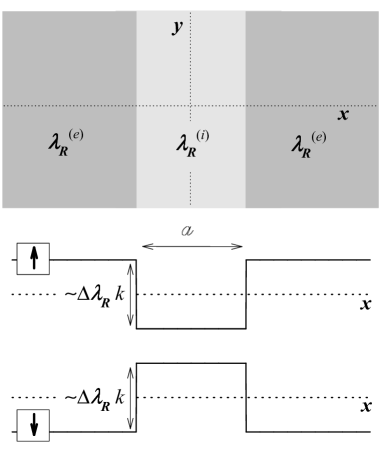
We consider a two-dimensional electron gas (2DEG) confined to a III-V quantum well whose inversion asymmetry produces an electric field in the perpendicular () direction. As a consequence of the relativistic corrections this electric field acts on the 2DEG carriers as an effective SO coupling field known as the Rashba term [9, 10]. The strength of the Rashba coupling depends on the heterostructure’s vertical electric field and has been shown to be experimentally controllable with a tunable gate voltage [11]. We take advantage of this tunability to define a heterostructure with a space modulated SO coupling intensity, depicted schematically in the upper part of Fig. 1. In practice, the SO coupling variation would correspond to a modulated electric field in the vertical direction. The well has a constant SO coupling strength except within a narrow region (guide) of width where it takes the ‘internal’ value .
We model the conduction electrons of this heterostructure using the effective mass Hamiltonian
| (1) |
where the modulated SO coupling reads
| (4) |
Equation (1) also contains the conduction band effective mass and the Pauli matrices and corresponding to the in-plane electron spin.
Since the Hamiltonian is translationally invariant in coordinate its eigenstates have well-defined momentum in that direction. In this representation the Hamiltonian is separable in space coordinates and the eigenstates are composed of a propagating longitudinal plane-wave, having momentum , and a spinorial transverse profile
| (5) |
where the spinorial part is given in the usual basis.
From the experimental data reported by Nitta et al. [11] for an In0.53Ga0.47As/In0.52Al0.48As heterostructure, we extract the following parameter values, to be used below in the numerical applications: , where is the free electron mass; eVcm; eVcm; relative dielectric constant of InGaAs ; -coordinate wavevector cm-1, near the Fermi wavevector of a 2DEG with density cm-2.
Before presenting numerical results with the above Hamiltonian and in order to clarify our purpose we consider the following simplification on Eq. (1): let us assume that the guide can have localized states in the coordinate having a characteristic transverse wavevector . Therefore, in a qualitative analysis, we can ignore the term containing . The eigenstates of the resulting approximated Hamiltonian have well defined spin in the direction and feel an effective spatial potential that depends on the eigenvalue, i.e., it changes sign from to spin orientation. Figure 1 depicts a schematic representation of the up and down potentials. It has to be noted that the depth of the effective potential well for and the height of the barrier for spin orientation depend both on the spin-orbit modulation step and the longitudinal wavevector of the state . As increases the attractive or repulsive character will also increase linearly.
The above analysis indicates that transverse space-confined modes can exist only for one of the two spin orientations thus showing the feasibility of selective spin guiding in this kind of heterostructures. We proof below that this conclusion remains valid when the term in Eq. (1) is taken into account. The -translational invariance of the eigenstates makes the initial two-dimensional Hamiltonian in coordinate space reduce to an effective one-dimensional one, corresponding to the transverse modes
| (6) |
We shall numerically obtain the relevant transverse eigenmodes of the Hamiltonian from the resolution of the time-dependent Schrödinger equation uniformly discretized in the coordinate and in time. The procedure is as follows: we evolve in time an initial spinorial wavepacket and, taking advantage of the harmonic time evolution for eigenmodes, we extract the transverse eigenspinors and eigenenergies using Fourier analysis of the time signals. For a certain value of -wavevector the time evolution of any wavepacket is decomposed as:
| (7) |
Besides the eigenenergies of the different transverse modes , Fourier transform at each grid point yields the local value of the eigenspinors. This method is appropriate to the present problem since an initial wavepacket inside the guide (see Fig. 1) will excite the confined transverse modes, if they exist, or it will quickly spread to the bulk surrounding the guide. We use Gaussian-shaped wavepackets in coordinate space with spin oriented in direction, i.e.,
| (8) |
with the eigenspinors
| (9) |
The spatial spread of the wavepacket is chosen close to the width of the spin-orbit guide because we want a maximum overlap with the confined transverse modes. Gaussian wavepackets are appropiate to excite confined modes having even parity in the coordinate while for odd parity states it is convenient to use an antisymmetric wavepacket. This can be done by multiplying Eq. (8) by .
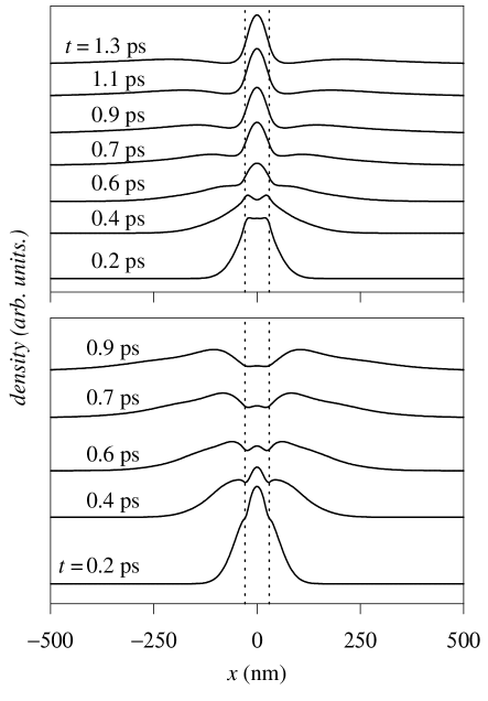
Physically, the input wavepacket represents an electron having well-defined and spin oriented along , injected from a lead with transversal dimensions matching those of the guide. Figure 2 shows the time evolution of the density for initial wavepackets with two different initial spin orientations: (up) and (down), using a guide width nm. It can be seen that for down initialization the wavepacket spreads over the transversal dimension in ps, with a complete depletion of density inside the spin guide. For spin up a part of the probability density remains confined to the guide as time evolves. This means that our initial up state was composed of confined and travelling transversal modes, while the down state is only composed of the latter ones. For a general orientation of the initial spin the confined fraction of the density depends on , vanishing if the initial spin points in the direction and reaching a maximum for the one.
To identify and extract the confined modes present in the time evolution simulation we use the mentioned Fourier analysis technique, focussing on a frequency region of the order . This analysis reveals that for our parameter set there is only one confined mode with spin polarization mainly oriented in direction, as was expected from the above discussion. To observe a second confined mode (antisymmetric), maintaining the width of 60 nm, the longitudinal wavevector should be increased up to cm-1. Actually, for a fixed the number of confined states depends only on the product . The probability and spin densities of the confined mode, related to the wavefunction by
| (10) | |||||
| (11) | |||||
| (12) |
are shown in Fig. 3.
Probability and spin densities clearly show the confining character of the guided mode, the main spin polarization being concentrated in direction. The mode has zero and a small . This confined mode is not an eigenstate of , as the transversal Hamiltonian does not commute with this operator but, nevertheless, it has an expectation value , very close to the value for eigenstates.
It is worth to mention that since time-reversal symmetry is conserved by the Hamiltonian of Eq. (1), Kramers degeneracy must hold. Therefore, a counterpart to the confined mode discussed above exists. This complementary state is also confined to the guide but its spin polarization and longitudinal momentum () are inverted, i.e., it is mainly oriented in direction and has .
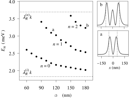
The ability of the guide to confine additional modes is enhanced by increasing the guide-width . Figure 4 shows the evolution with , maintaining to the same value as before. Confined modes should lie between the energy edges of the guide, marked in Fig. 4 by dotted lines. We note that the second and third modes appear for guide widths of and nm, respectively, with probability densities having an additional node for each successive mode. As the first state these higher modes have spin almost completely oriented in direction.
The confining energies of the guide are of order , which takes a value of meV for our parameter set. Consequently, the practical operation of the proposed guide is limited to low temperatures, since the coupling with phonons in the meV range would reduce the efficiency of the guiding effect. In this sense, it has to be pointed out that the assignment of a lower spin-orbit constant to the guide region is not arbitrary, because, as reported by Nazarov et al. [12], spin-orbit coupling induces an admixture of pure up and down spin orientations in the eigenstates that causes spin decay through phonon emission, shown to be the dominant spin decoherence source for quantum dots. To minimize the effects of this mechanism the confining structure needs to have the minimum spin-orbit coupling.
In summary, we have shown that a guide structure in a semiconductor quantum well, defined by a spatially modulated Rashba spin-orbit coupling, gives rise to transverse-confined and longitudinal-propagating modes only for a given spin orientation. This feature characterizes the proposed structures as spin guides that constitute natural paths to distinguish and drive the spin of the carriers within semiconductors. The feasibility of this spin-guiding mechanism is limited to low temperatures as the energies of the Rashba effect are in the range of a few meV’s.
This work was supported by Grant No. BFM2002-03241 from DGI (Spain).
REFERENCES
- [1] D. Loss, D. P. DiVincenzo, Phys. Rev. A 57, 120 (1998).
- [2] S. A. Wolf, D. D. Awschalom, R. A. Buhrman, J. M. Daughton, S. von Molnár, M. L. Roukes, A. Y. Chtchelkanova, D. M. Treger, Science 294, 1488 (2001).
- [3] S. Datta and B. Das, Appl. Phys. Lett. 56, 665 (1990).
- [4] T. Koga, J. Nitta, H. Takayanagi, S. Datta, Phys. Rev. Lett. 88, 126601 (2002).
- [5] M. Governale, D. Boese, U. Zülicke, C. Schroll, Phys. Rev. B 65, 140403 (2002).
- [6] J.M. Kikkawa and D.D. Awschalom, Phys. Rev. Lett. 80, 4313 (1998).
- [7] R. Fiederling, M. Keim, G. Reuscher, W. Ossau, G. Schmidt, A. Waag, L. W. Molenkamp, Nature (London) 402, 787 (1999); Y. Ohno, D. K. Young, B. Beschoten, F. Matsukura, H. Ohno, D. D. Awschalom, Nature (London) 402, 790 (1999).
- [8] H. J. Zhu, M. Ramsteiner, H. Kostial, M. Wassermeier, H. P. Schönherr, and K. H. Ploog, Phys. Rev. Lett. 87, 016601 (2001).
- [9] E. I. Rashba, Fiz. tverd. Tela (Leningrad) 2, 1224 (1960) [Sov. Phys. Solid State 2, 1109 (1960)].
- [10] W. Knap, C. Skierbiszewski, A. Zduniak, E. Litwin-Staszewska, D. Bertho, F. Kobbi, J. L. Robert, G. E. Pikus, F. G. Pikus, S. V. Iordanskii, V. Mosser, K. Zekentes, Yu. B. Lyanda-Geller, Phys. Rev. B 53, 3912 (1996).
- [11] J. Nitta, T. Akazaki, H. Takayanagi and T. Enoki, Phys. Rev. Lett. 78 1335 (1997).
- [12] A. V. Khaetskii, Y. V. Nazarov, Phys. Rev. B 64, 125316 (2001).