Improved Light Absorption by Quantum Confinement and Band
Folding: Enhanced Efficiency in Silicon Based Solar Cells
Abstract
The improvement of light absorption in Si/BeSe0.41Te0.59 heterostructures for solar cell applications is studied theoretically. First, using simple approaches we found that light absorption could be improved in a single (uncoupled) quantum well with a thickness up to 20 Å. Second, by semiempirical tight-binding methods we calculated the electronic structure and optical properties of various (Si/(BeSe0.41Te [001] superlattices. Two bands of interface states were found in the band gap of bulk Si. Our calculations indicate that the optical edges are close to the fundamental band gap of bulk Si and the transitions are optically allowed.
pacs:
73.21.Cd,73.21.Fg,78.67.DeI Introduction
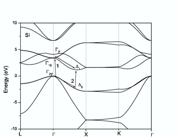
Silicon is the principal material for integrated circuits. Not only is the band gap (1.12 eV) ideal for room temperature operation, but also the oxide (SiO provides the necessary flexibility to fabricate millions of devices on a single chip. High integration implies high-speed operation that is limited by the interconnect propagation delay of the signal between devices. This constraint suggests that the integration of Si micro-electronics might be aided by optical interconnection. Unfortunately, silicon does not respond strongly to optical exitations because it is an indirect band gap semiconductor: the band extrema for electrons and holes are located at different points in the Brillouin zone (Fig. 1). Therefore, intrinsic formation or recombination of electron-hole pairs becomes a three-particle event, which is weaker than a two-body process.
There has been a tremendous effort in exploring ways of breaking the silicon lattice symmetry and mixing different momentum states in order to induce optical gain Iyer and Xie (1993); Tsu (1993). The radiative efficiency depends on the competition between non-radiative fast processes and relatively slow radiative processes. To optimize the efficiency we have to eliminate non-radiative channels by having high purity materials and increase the oscillator strength of radiative channels. The above criteria also apply to photovoltaics.
One modality for improving the optical response is quantum confinement. Confinement of the charge density in quantum wells (QWs) permits the relaxation of the optical selection rules for interband transition. In addition, the band folding in superlattice (SL) structures will enhance the absorption. Consequently a Si based SL will reduce the symmetry which translates into band folding toward the zone center; and as a result vertical transitions will be available at energies closer to the indirect band gap.
Beryllium-chalcogenides are good candidates for Si-based heterostructures. They are wide-band gap zinc blende semiconductors with lattice constants close to that of Si. Thus BeTe and Be Se have the lattice constants of 5.6269 and 5.1477 Å, respectively, 3.6 % larger and 5.2 % smaller than Si. Vegard’s law indicates that the lattice matched composition with Si is BeSe0.41Te0.59. Recent developments Clark et al. (2000); Kirk et al. (2000) in the growth of silicon lattice-matched BeSe0.41Te0.59 open the opportunity for a new class of Si based devices.
We analyze quantum confinement and band folding in silicon based heterostructures (Si/BeSeTe heterostructures) as ways of enhancing light absorption and, therefore, improving the efficiency of solar cells. In this study we use a semiempirical tight-binding (TB) method Slater and Koster (1954). In section II we present the tight binding parameters of BeTe and BeSe, fitted to first principles calculations. The model is that of Vogl et al. Vogl et al. (1983) modified according to Chadi Chadi (1977) as to include the spin-orbit interaction. The bulk TB parameters of BeSe0.41Te0.59 are considered as virtual-crystal approximation of constituent materials. The TB parameters of silicon are those of Vogl et al. Vogl et al. (1983) adapted to include the spin–orbit coupling. In section III we discuss some methods to improve the light absorption in Si based heterostructures such as quantum confinement in a single (uncoupled) QW and band folding in SL structures. A significant increase in direct absorption is obtained for a narrow uncoupled silicon QW. However, thin barriers are also required in order for carriers to move across the structure. In this spirit, we calculate the electronic and optical properties of Si/BeSeTe SLs using the mentioned TB method. In the last section the conclusions are outlined.
II Nearest neighbor Tight-Binding parameters of beryllium chalcogenides
Since both Si and BeSe0.41Te0.59 are indirect band materials, full band calculations are required for the theoretical understanding of electron transport and optical properties in such heterostructures. For this purpose we use the empirical tight-binding (ETB) method as one of the most used tools in research of complex molecular and solid-state systems Harrison (1980). Despite the fact that ETB is based on physical approximations such as a one-particle picture, short-range interactions, etc. (aposteriori justified, however), it gives fast and satisfactory results. In terms of accuracy, it lies between the very accurate, very expensive ab-initio and the fast but limited-accuracy empirical methods. TB techniques are increasingly employed in structures like resonant tunneling diodes, QWs, and SLs. They are more complete than envelope-function or kp methods because they incorporate the entire band structure of the constituent bulk materials in a transparent manner. Also the short-range nature of the model is suitable for modeling heterointerfaces which are present in such quantum structures. In ETB models the electronic wave functions are expanded as a linear combination of atomic orbitals. The real attractiveness resides in the great versatility of the method that can be used for a variety of physical situations like: (i) molecular models based on linear combination of atomic orbitals with strong directional properties; (ii) calculation of electronic states in unknown systems based on transferability of the Hamiltonian matrix elements as determined in known cases (i.e. transferability of the Hamiltonian matrix elements from bulk semiconductors to low dimensional systems like QWs, quantum dots, etc.); (iii) quantitative predictions of physical properties (like fitting the band structure of a semiconductor to ab-initio and experimental data and using those parameters to calculate optical properties of the same semiconductor). The last two points will be used in this paper.
One of the most popular TB models is the sp model Vogl et al. (1983). This is a twenty-band model if spin-orbit coupling is included Chadi (1977). The presence of additional orbital is able to reproduce the band gap in indirect semiconductors like silicon. The TB parameters of silicon are those from Vogl et al. Vogl et al. (1983) augmented with spin-orbit coupling according to Chadi Chadi (1977).
BeTe and BeSe are quite new materials in the sense that there are few experimental facts about these semiconductors. The bulk TB parameters of BeTe and BeSe are determined by fitting the ab-initio calculations of Fleszar and Hanke Fleszar and Hanke (2000). Virtual-crystal approximation (VCA) is used to determine the TB parameters of BeSe0.41Te0.59 . The approximation is expected to work well because BeTe and BeSe crystallize in zinc-blende structures and have similar band structures. The nearest neighbor parametrization in the sp model requires 15 parameters including spin-orbit interaction. The spin-orbit coupling was included due to the large spin-orbit splitting of the valence band, of about 0.45 eV for BeSe and 0.96 eV for BeTe. To find the nearest neighbor parametrization we used a similar procedure to Ref. Yamaguchi, 1987. The procedure is more consistent than that presented in Ref. Vogl et al., 1983. We adapted the procedure in order to consider spin-orbit coupling. The results are shown in Table 1.
| BeTe | BeSe | BeSe0.41Te0.59 | |
| E(s,c) | 5.11241 | 5.56003 | 5.295934 |
| E(s,a) | -15.40059 | -14.95297 | -15.2171 |
| E(p,c) | 4.42741 | 5.02603 | 4.672844 |
| E(p,a) | -0.29859 | 0.30003 | -0.05316 |
| E(s*,c) | 30.16 | 21.666 | 26.67746 |
| E(s*,a) | 39.203 | 24.433 | 33.1473 |
| V(s,s) | -3.303 | -8.195 | -5.30872 |
| V(sc,pa) | 4.423 | 5.633 | 4.9191 |
| V(sa,pc) | 5.511 | 4.89 | 5.25639 |
| V(x,x) | 0.331 | 1.531 | 0.823 |
| V(x,y) | 6.362 | 6.324 | 6.34642 |
| V(s*a,pc) | 11.503 | 7.462 | 9.84619 |
| V(s*c,pa) | 3.11 | 4.572 | 3.70942 |
| 0.97 | 0.499 | 0.77689 | |
| 0 | 0 | 0 |
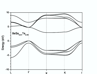
The focus of these calculations was to find the best parameters that reproduce the valence band edges ( and and conduction band edge at and X. The reproduction of band edges at the zone center of the valence and conduction bands and the band gap between valence band and conduction band is within 3% error. The spin-orbit coupling for Be was chosen to vanish, because Be is a light element and its spin-orbit coupling is negligible. This is also consistent with the spin-orbit splitting of 0.1 eV for another Be-chalcogenide, BeS with the sulfur atom, lighter than selenium and tellurium atoms. The energy band diagram for BeSe0.41Te0.59 is shown in Fig. 2. The material appears to be indirect band gap with the conduction band minimum at the point. The predicted band gap is 2.97 eV. Previous measurements Clark et al. (2000) indicate a conduction band offset of 1.2 eV for the Si/BeSe0.41Te0.59 heterostructure. This leaves a valence band offset of about 0.65 eV for the Si/BeSe0.41Te0.59 heterostructure. The TB parameters and the valence band offset will be used in the next section in order to calculate electronic and optical properties of the Si/BeSe0.41Te0.59 SL.
III Improved Optical Absorption by Quantum Confinement and Band Folding
III.1 A Single Quantum Well
The absorption edges in bulk silicon are indirect and the jumping of the electron from valence band (VB) to conduction band (CB) is assisted by a phonon (in electron transitions from VB to CB the k momentum must be conserved). The band structure of Si is shown schematically in the Fig. 1. The indirect band gap is . The absorption process involves two steps, one is electron-photon interaction and the other is electron-phonon interaction. Basically we have two processes denoted by 1 and 2. In process 1 an electron is first excited to the state and then by an emission of a phonon the electron arrives in the CB state. Similarly for process 2, however, in this process it starts with an emission of a phonon. Mathematically, the transition probability is given by Fermi’s Golden Rule for second order perturbation
| (1) |
where represents the initial state, the intermediate state and the final state. and are the Hamiltonians for electron-phonon and electron-photon interaction, respectively. The energies and are the energies for photons and phonons, respectively. The second sum on the right-side hand is the oscillator strength of the transition. For this reason, there is a long absorption tail between 1.12 eV and and about 3 eV that reflects the indirect nature of the band gap. The sharp rise in absorption with increasing photon energy starting around 3.2 eV (380 nm) is associated with the direct transition at point ( whose energy is 3.4 eV (365 nm).
In direct band gap materials light absorption in 2D systems is formally similar to 3D systems. Although the light absorption in indirect band gap 2D systems looks to be similar to 3D systems, this is not the case. The absorption coefficient for an uncoupled Si/ BeSe0.41Te0.59 QW has basically three components Hybertsen (1994)
| (2) |
where is a constant, gives the direct bandgap contribution and gives the phonon assisted contribution with 1-phonon absorption, and is the phonon assisted contribution with 1-phonon emission. Basically,
| (3) |
| (4) |
is the bulk dipole matrix element between bands, is the matrix element contribution from electron-phonon interaction, and is the overlap between the envelope-functions at different Brillouin points:
| (5) |
where k0 is the location in space of each conduction valley. For silicon, if is the growth direction, then the 2 valleys along z-directions (with are responsible for direct transitions. The other four valleys contribute to phonon-assisted absorption. For infinite wells the overlap integral has the behavior depicted in Fig. 3. For very narrow QW’s the overlap integral tends to one, which means that in a genuine 2D system only the transverse momentum has to be conserved. For the other asymptotic limit, i.e. very wide well, the overlap integral vanishes. In physical terms, this says that the system became genuinely 3D and any electromagnetic transition has to be vertical in the absence of phonons. Moreover, from Fig. 3 we may expect to have a strong direct transition (with an overlap integral no less than 0.1) for a QW with a width up to 20 Å, i.e. an ultrathin QW. In the following we will discuss the possibility of improving the oscillator strength in Si/ BeSe0.41Te0.59 based SLs.

III.2 Electronic Structures of (Si2)n/(BeSe0.41Te0.59)m [001] Superlattices
The use of SL structures relaxes the condition of ultrathin QW. However, the SL has to have thin barriers. Thin barriers allow photo-generated carriers to be swept away by the built in electric field without recombination. Thicker barriers induce localization of carriers and implicitly higher recombination rate. The alternation of QWs and barriers along [001] growth axis will generate a band folding in the SL and band mixing of zone-center and zone edge states Gell et al. (1986); Schulman and Chang (1985). The band mixing will inherently enhance the oscillator strength for direct transition in Si structures. On the other hand, band folding will induce states to which vertical transitions are possible at energies by far lower than 3.4 eV, the lowest energy for vertical transitions in bulk Si.
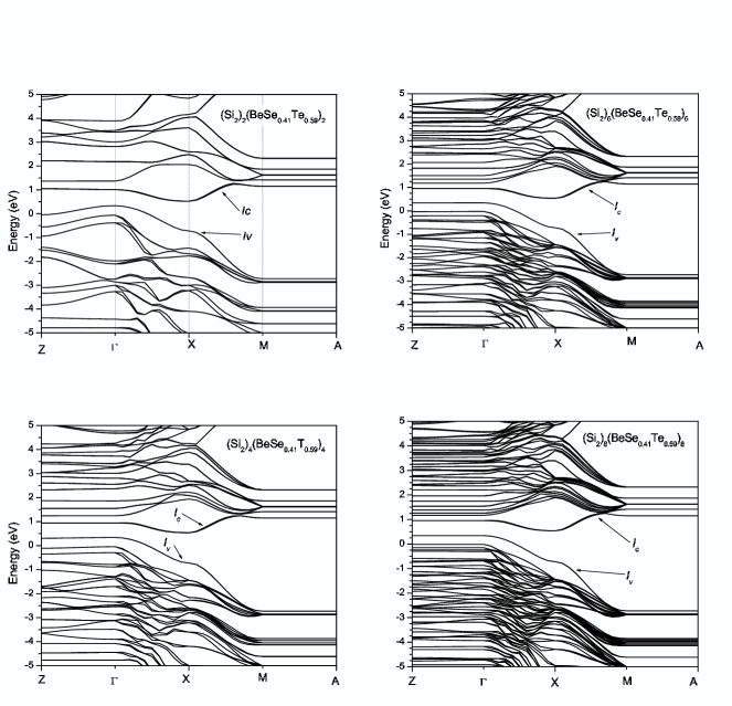
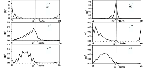
We consider a Si/BeSe0.41Te0.59 SL whose layers are perpendicular to [001] direction. We employ the nearest neighbor sp TB Hamiltonian including spin-orbit interaction. We denote this SL as a (Si/(BeSe0.41Te SL with two-atom thick layers of Si and two-atom thick layers of BeSe0.41Te0.59 repeated periodically. The defined supercell consists of 2 ( adjacently bonded atoms Si, Si, …..Si, Be, Te/Se, Be, Te/Se, …..Be, Te/Se. The TB matrix elements of the Si/BeSe0.41Te0.59 SL are taken over directly from those bulk values. The on-site energies of the BeSe0.41Te0.59 are accordingly changed to match the valence band offset at the interface. Simple averages were used to supply the parameters connecting different materials at the interface. Since the spin orbit must be included the SL Hamiltonian will be represented as having functions. Once the TB matrix elements have been established the SL band structure reduces to the diagonalization of the matrix Hamiltonian. The band structure of (Si/(BeSe0.41Te SL for , , , and are displayed in Fig. 4. The zero of energy corresponds to the top of the valence band in bulk Si. The band folding effect can be seen as many crowded subbands. Two interface bands ( and , one empty and one occupied, were found. They lie in the lower and upper parts of the band gap of bulk silicon, respectively. The origin of these interface bands rests on the polar nature of the interface as was also found in GaAs/Ge SL Saito and Ikoma (1992). The polarity of the interface originates from the large differences in the on-site energies for the constituent atoms (Si and Be or Se/Te). Even if a (110) non-polar interface is used, one interface band is still found in II-VI/IV SLs Wang and Ting (1995); Wang (1996). We calculated the planar charge density of some of the occupied and empty band edge states of the SL with at point in the Brillouin zone. The planar charge density of some of the band edge states and interface states are depicted in Fig. 5 for the SL with . By interface states we mean states which die away within few layers from the interface. We denote by , the interface states of the band and by , the interface states of the band at point. The charge density of the interface state has a maximum at the Be-Si interface, while the next occupied state is confined, but still is localized toward the Si-Se/Te interface. Only the third occupied state is genuinely confined in silicon slab. The charge density of the interface state has a maximum at the Si-Se/Te interface, while the next empty state is confined, but still is localized toward the Si-Be interface. Again, only the third empty state is genuinely confined in silicon slab. We believe that this is associated with acceptor behavior of Be and donor behavior of Se and Te with respect to Si Sze (1980).
III.3 Optical Properties of (Si2)n/(BeSe0.41Te0.59)m [001] Superlattices
The electronic contribution to absorption spectrum is given by , where is the absorption coefficient and Harrison (1980)
| (6) |
is the imaginary part of dielectric function. Here is the electron mass, is the volume, is the electron charge, is the Planck constant and is the oscillator strength for the direct transition from the state to , with the photon momentum neglected. The oscillator strength is defined as
| (7) |
In Eq. (7) and are the valence and conduction band, eigenstates, and are their corresponding energies, is the polarization of light, and p is the momentum operator. In the empirical tight-binding approach the momentum matrix element is defined as Graf and Vogl (1995)
| (8) |
Because the variation of the oscillator strength over the Brillouin zone is small Schulman and Chang (1985), we first calculate the joint densities of states (JDOS). We assume that light is propagating along the SL growth direction. The JDOS represents the number of states that can undergo energy and k-conserving transitions for photon frequencies between and . The JDOS associated with Eq. (6) are shown in Fig. 6 for SLs with , , , and . A 0.05 eV broadening was considered for each electronic energy. The summation over Brillouin zone was replaced by the summation over special points in the Brillouin zone Chadi and Cohen (1973); Ren and Dow (1988).
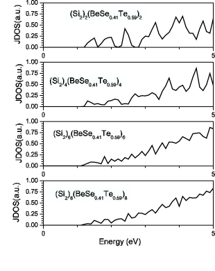
Due to band folding the absorption edges for vertical transitions are lowered toward the indirect band gap of bulk Si. Moreover, the curves rise slowly and, with increasing , the absorption edges extend to lower energies. Similar results were found in the calculations for porous Si with periodic boundary conditions Cruz (1999). Eq. (6) tells us that the strength of the optical absorption is also determined by the oscillator strength. We denote by V1, V2, and V3 the first three top valence subbands, and by C1, C2, and C3 the first three conduction subbands. We calculated the oscillator strengths of several interband transitions relative to the oscillator strength of the direct transition in bulk Si. The results are shown in Fig. 7 for . The oscillator strengths of interband transitions are at least 10 times smaller than their bulk counterpart and basically range from 10 to 10 -1 relative to transition in bulk Si. The strongest transitions are those coming from the third confined hole level to the second and third confined electron levels.

IV Conclusions
We studied light absorption of silicon-based heterostructures (Si/BeSe0.41Te that might be used in solar cell applications. We found that significant absorption occurs for thin uncoupled quantum wells with their width up to 20 Å. We also studied the (Si)n/(BeSe0.41Te superlattice structures with a semiempirical tight-binding method. In order to perform the superlattice calculations, we determined the tight-binding parameters for BeSe and BeTe in the sp nearest neighbor model including spin-orbit interaction. Electronic structure and optical properties were calculated for various superlattice structures. Two interface bands were found to exist in the band gap of bulk silicon. We found that band folding induces vertical transitions near the indirect band gap of bulk Si. In addition, calculated oscillator strengths for vertical transitions near the optical band edge show the mixing of the zone-center and zone edge states of bulk Si for conduction subbands. Therefore, the transitions are optically allowed and the response of silicon based heterostructures to illumination is enhanced.
Acknowledgements.
This work was supported in part by NASA grant NCC3-516 and by the Texas Advanced Technology program under grant No. 003594-00326-1999.References
- Iyer and Xie (1993) S. S. Iyer and Y. H. Xie, Science 260, 40 (1993).
- Tsu (1993) R. Tsu, Nature 364, 338 (1993).
- Clark et al. (2000) K. Clark, E. Maldonado, P. Barrios, G. F. Spencer, R. T. Bate, and W. P. Kirk, J. Appl. Phys. 88, 7201 (2000).
- Kirk et al. (2000) W. P. Kirk, K. Clark, E. Maldonado, N. Basit, R. T. Bate, and G. F. Spencer, Supperlatt. Microstruct. 28, 377 (2000).
- Vogl et al. (1983) P. Vogl, H. P. Hjalmarson, and J. D. Dow, J. Phys. Chem. Solids 44, 365 (1983).
- Slater and Koster (1954) J. C. Slater and G. F. Koster, Phys. Rev. 94, 1498 (1954).
- Chadi (1977) D. J. Chadi, Phys. Rev. B 16, 790 (1977).
- Harrison (1980) W. A. Harrison, Electronic Structure and the Properties of Solids (Freeman, San Francisco, 1980).
- Fleszar and Hanke (2000) A. Fleszar and W. Hanke, Phys. Rev. B 62, 2466 (2000).
- Yamaguchi (1987) E. Yamaguchi, J. Phys. Soc. Jpn. 56, 2835 (1987).
- Hybertsen (1994) M. S. Hybertsen, Phys. Rev. Lett. 72, 1514 (1994).
- Gell et al. (1986) M. Gell, D. Nino, M. Jaros, and D. C. Herbert, Phys. Rev. B 34, 2416 (1986).
- Schulman and Chang (1985) J. N. Schulman and Y. C. Chang, Phys. Rev. B 31, 2056 (1985).
- Saito and Ikoma (1992) T. Saito and T. Ikoma, Phys. Rev. B 45, 1762 (1992).
- Wang (1996) E. G. Wang, Appl. Surf. Sci. 105/105, 626 (1996).
- Wang and Ting (1995) E. G. Wang and C. S. Ting, Phys. Rev. B 51, 9791 (1995).
- Sze (1980) S. M. Sze, Physics of Semiconductor Devices (John Wiley and Sons, New York-Chichester-Brisbane-Toronto, 1980), 2nd ed.
- Graf and Vogl (1995) M. Graf and P. Vogl, Phys. Rev. B 51, 4940 (1995).
- Chadi and Cohen (1973) D. J. Chadi and M. L. Cohen, Phys. Rev. B 8, 5747 (1973).
- Ren and Dow (1988) S. Y. Ren and J. D. Dow, Phys. Rev. B 38, 1999 (1988).
- Cruz (1999) M. Cruz, Phys. Rev. B 59, 15381 (1999).