Quasiparticle Calculations for Point Defects on Semiconductor Surfaces
Abstract
We discuss the implementation of quasiparticle calculations for point
defects on semiconductor surfaces and, as a specific example,
present an ab initio study of the electronic structure
of the As vacancy in the +1 charge state on the GaAs(110)
surface. The structural properties are calculated with the
plane-wave pseudopotential method, and the quasiparticle
energies are obtained from Hedin’s approximation.
Our calculations show that the 1a′′ vacancy state in the band gap
is shifted from 0.06 to 0.65 eV above the valence-band maximum
after the self-energy correction to the Kohn-Sham eigenvalues. The result
is in close agreement with a recent surface photovoltage imaging measurement.
PACS: 71.15.-m; 71.45.Gm; 73.20.Hb
1 Introduction
Over the past 15 to 20 years intense research efforts have been made to understand the nature of native point defects near and at semiconductor surfaces. Such defects play an important role in surface electrical characteristics, e.g., Fermi-level pinning and charge-carrier recombination. They also influence the kinetics of adsorption, diffusion, and growth as well as surface chemical activity. The progress of the research efforts in understanding point defects on III–V semiconductor surfaces has recently been reviewed by Ebert [1].
At the atomistic level significant insight into the identification of these defects comes from scanning tunneling microscopy (STM). However, STM measures the local electronic density of states, which cannot always be directly interpreted as the atomic geometry. Therefore, accurate calculations have turned out to be very valuable for the interpretation of the experimental findings. In this paper we present an ab initio study of the arsenic vacancy on the GaAs(110) surface under p-type conditions. In STM images of the filled-state As sublattice, this vacancy gives rise to two distinct features: a dark hole of the lateral dimension of one As dangling bond and a long-range charge-related depression of the neighbouring As atoms [2]. The first feature is directly related to the missing atom, and the second one is due to a downward local band bending, from which it was concluded that in p-GaAs the arsenic vacancy is positively charged. STM images acquired under positive bias probe the empty pz orbitals of the Ga sublattice and show an enhancement of the contrast from the two Ga atoms nearest to the vacancy. Lengel et al. [2] interpreted their finding as an outward relaxation of the two Ga atoms neighbouring the vacancy. They also found support for this interpretation from a tight-binding calculation. Their calculation suggested a charge state of +2 for the vacancy. On the other hand, by comparing STM images of the arsenic vacancy with the images of Zn dopant atoms on p-type GaAs(110), Chao et al. [3] were able to determine the charge state of to be +1, utilizing the fact that the dopant atom is in a charge state of a priori.
Recent density-functional theory (DFT) calculations by Zhang and Zunger [4] and by Kim and Chelikowsky [5, 6] have confirmed the stability of the +1 charge state. Furthermore, their calculations have independently shown that the energy minimization of the defect geometry results in a downward relaxation of the neighbouring Ga atoms, and the calculated STM images show an enhancement of these two atoms in agreement with experiment. Both of these calculations were performed at a comparable level of sophistication but differed in the details. Zhang and Zunger [4] found an asymmetric relaxation of , whereas Kim and Chelikowsky [5, 6] found a symmetric relaxation, which seems to agree with experiment. However, in a recent combined experimental and theoretical study on a related system, the phosphorus vacancy on InP(110), Ebert et al. [7] suggested that the symmetric feature of the experimental STM image could also be explained by a thermal flip motion from two degenerate asymmetric configurations.
For properties other than structural ones the experimental situation is less complete. There are so far no direct measurements of either defect ionization or charge-transfer levels for on GaAs(110). Indirect information about these quantities can be obtained, for instance, from measurements of the local band bending. Both the ionization and charge-transfer levels can be calculated theoretically, but so far this has not been done beyond DFT and using the local-density approximation (LDA). Furthermore, we note that the reported values deviate among the different studies. DFT-LDA also suffers from the underestimation of the fundamental band gap, which introduces a large uncertainty when interpreting the Kohn-Sham eigenvalues of defect levels that lie inside the band gap as actual energy levels. As we will show in this paper, the band-gap problem for defect states can be circumvented by employing the approximation [8] for the electronic self-energy and calculating the proper quasiparticle energies. The approximation has previously been applied to the perfect GaAs(110) surface [9, 10] as well as to bulk defects in some other materials, such as the Li vacancy in LiCl [11] and the oxygen vacancy in zirconia [12], with good agreement between the theoretical predictions and the available experimental data. We note in passing that all the mentioned studies relied on plasmon-pole models, whereas our study takes the full frequency dependence of the screened Coulomb interaction into account.
2 Method and Computational Details
2.1 Atomic geometry
The ground-state properties, such as the geometric structure of the defect, are calculated using DFT [13, 14] and the plane-wave pseudopotential method as implemented in the FHImd code [15, 16]. The exchange-correlation functional is treated in the local-density approximation as parametrized by Perdew and Zunger [17]. The single-particle orbitals are expanded in plane waves with a cutoff energy of 10 Ry in most of the calculations, but convergence tests were performed up to a cutoff of 15 Ry. With the basis set used we find the bulk lattice constant to be 5.55 Å (neglecting zero-point vibrations), which is in agreement with other calculations for III–V semiconductors [6, 18, 19] and 1.8% smaller than the experimental value at room temperature of 5.65 Å [20].
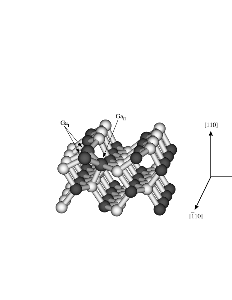
The As vacancy on GaAs(110), whose geometry is shown in Fig. 1, is described using the supercell method with periodic boundary conditions. The supercell slab consists of a 42 surface unit cell with six atomic layers, with one As atom missing in the top layer, and four vacuum layers. The dangling bonds at the bottom of the slab are passivated by pseudoatoms with noninteger nuclear charges of 0.75 and 1.25 for As and Ga termination, respectively. We allow the atoms in the top three layers to fully relax while keeping the atoms in the three bottom layers at their theoretical bulk positions. In the case of the positively charged defect we apply a uniform compensating charge throughout the unit cell in order to maintain overall charge neutrality. The integration in reciprocal space was done using the special -point [21] in the irreducible part of the Brillouin zone.
In order to test the influence of the supercell size we also performed a series of investigations using smaller 22 and 21 unit cells and found that the dispersion of the defect level, due to the spurious interaction of the defect with its periodic images, changed from 0.6 eV (22) to 1.5 eV (21), compared to 0.3 eV in the case of the 42 unit cell. For the 21 unit cell the defect–defect interaction is so strong that the two defect levels in the band gap exhibit a crossing, thus making any further calculations using such a small unit cell doubtful. On the other hand, the 22 unit cell gave results consistent with the ones obtained for the larger 42 cell. In particular, the formation energy for the neutral defect turned out to be the same using either of the unit cells.
Furthermore, we did a series of comparisons between six-layer slabs and four-layer slabs for the 22 unit cell and found no significant differences in the defect band structures (dispersion relations) for any of the possible charge states +1, 0, or . In the case of the four-layer slab only the top two layers were relaxed in the geometry optimization.
2.2 Quasiparticle energies
Green-function theory is a mathematical framework for calculating the actual quasiparticle band structure, i.e., electron addition and removal energies, which characterize the excitation from an -particle system to an (1)-particle system during a photoemission process. These energies, , are in principle given exactly by the quasiparticle equation
| (1) |
where is the external potential, the Hartree potential, and the quasiparticle wave function. denotes the self-energy operator, which contains all contributions from dynamic exchange and correlation. In general the self-energy is nonlocal, energy-dependent, and has a nonzero imaginary part, whose inverse is proportional to the lifetime of the excited state. For real systems cannot be calculated exactly and must be approximated by a suitable functional expression. In the approximation is given by [8]
| (2) |
where is the one-particle Green function and the dynamically screened Coulomb interaction. All operators are here written in real space and imaginary time. This representation has the advantage that the self-energy is a simple product, which is exploited in the space-time method [22, 23] that we have used for our calculations. It avoids the multidimensional convolutions in reciprocal space and on the frequency axis that must be evaluated in conventional implementations. The inclusion of dynamic screening in the self-energy describes the correlation hole around individual electrons due to the Coulomb interaction. In this way the approximation goes beyond Hartree-Fock theory, which only describes exchange effects and ignores the correlation of electrons with different spin. Instead of simplified plasmon-pole models, which have been employed in almost all calculations for surfaces so far, we use the random-phase approximation with the full frequency dependence for the screened Coulomb interaction. At the end of the calculation the self-energy is Fourier transformed and analytically continued to the real energy axis.
As usual, also in our calculations the Green function is obtained from the Kohn-Sham eigenfunctions, incorporating a large number of unoccupied states. The LDA wave functions form a reasonable starting point for the study of electronic band structures and are obtained from an equation closely resembling Eq. (1), with the local exchange-correlation potential, , in the place of the self-energy. The quasiparticle energies are therefore calculated from first-order perturbation theory according to
| (3) |
where is the corresponding LDA eigenvalue associated with the wave function .
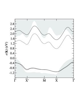
Before investigating the system we first perform accurate convergence tests for the perfect surface, which can be represented with a smaller 11 surface unit cell. Fig. 2 shows the quasiparticle band structure for the GaAs(110) surface. The dashed lines are obtained from DFT-LDA with a cutoff energy of 15 Ry, and the solid lines are the quasiparticle energies. The projected bulk band structure is indicated in grey. The ground-state density used for the DFT band-structure calculation was obtained using four special Monkhorst-Pack -points [24], which ensures the same Brioullin-zone sampling as a single -point for the larger 22 unit cell. The self-energy operator was evaluated at the four high-symmetry -points (,X̄,M̄,X̄’). The LDA surface bands are matched to the projected bulk bands by aligning the electrostatic potential in the central region of the surface slab with that of the bulk. The approximation has only a small effect on the dispersion of the occupied surface band and does not change its relative distance to the valence-band edge at . The and LDA occupied surface bands are hence aligned at this point. From Fig. 2 we then observe an almost uniform upward shift of the corrected unoccupied surface band by 0.8 eV, which is in close agreement with Zhu et al. [9] and 0.1–0.2 eV less than found by Pulci et al. [10]. This opening of the gap makes for the typical improvement of quasiparticle band structures over DFT-LDA for the unoccupied states. We also note that the shift in the surface band is similar to the shift we find for the conduction bands in the bulk, 0.7 eV, illustrating the similarity of the wave-function character between the surface states and the bulk valence and conduction bands. The filled surface state at and in the vicinity of the -point appears as a surface resonance, i.e., hybridization with extended bulk states is noticeable, and the peak becomes broad. The band structure at this point is shown for the sole purpose of illustrating the LDA and alignment. We repeated the calculations using different cutoff energies and found that the shift of 0.8 eV remained for 13, 11, and 10 Ry cutoff. Also, for a four-layer slab we obtained a correction of 0.8 eV, and at 10 Ry cutoff we investigated the sensitivity of the corrected band structure to variations in the number of unoccupied bands. The self-energy is fully converged if 1049 unoccupied bands are included. The difference in the quasiparticle energies around the band gap is less than 0.05 eV when the number of unoccupied bands is reduced to 153. With 379 unoccupied bands the agreement is better than 0.02 eV, which suffices for our purpose. For the calculation of the defect levels in the 22 surface unit cell we hence use 1500 unoccupied bands, which correspond to 379 bands in the case of a 11 cell.
3 Results and Discussion
3.1 Structural properties
Let us first recall the structure of the perfect GaAs(110) surface, which corresponds to the defect-free right-hand part of Fig. 1. This surface belongs to the C1h point group, which consists of a single mirror plane perpendicular to the [1̄10] direction. The relaxation of the surface preserves the point-group symmetry and consists chiefly of an inward movement of the Ga atom and an outward movement of the As atom. Hence the relaxation can be characterized mainly as a pure bond rotation, which results in a buckling of the surface [18]. The Ga atoms rehybridize from an sp3 to an sp2 bonding situation to form a locally planar structure. The empty pz-like orbital perpendicular to this plane forms the unoccupied surface band. The As atom maintains its sp3 hybridization and binds to three Ga atoms in a pyramidal arrangement with a nonbonding electron pair in the fourth direction pointing away from the surface. The filled surface band is composed from the As lone electron pairs.
We now turn the discussion to the As vacancy. The removal of the As atom leaves a dangling bond on each of the three Ga atoms surrounding the vacancy. As mentioned earlier, there is conflicting evidence for [4, 7] and against [5, 6] a breaking of the mirror symmetry due to the relaxation of the positively charged anion vacancy, which requires further careful studies. In this work we choose the second scenario and perform a relaxation of with the constraint that the C1h symmetry is preserved. The calculated equilibrium geometry shows a downward relaxation of the two Ga atoms in the first layer (GaI) and an upward movement of the second-layer Ga atom (GaII), which forms two new weak bonds with the GaI atoms. Thus the coordination of GaII is increased to five. In Fig. 1 the GaI and GaII atoms are indicated by arrows. We find the bond length between GaI and GaII to be 2.89 Å for , which is slightly longer than the value of 2.78 Å reported in Ref. [5]. When going from to , the GaI–GaII bond length decreases, indicating the bonding character of the 1a′′ defect level.
3.2 Electronic properties
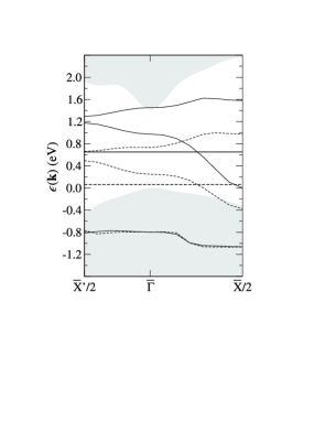
The arsenic vacancy gives rise to three electronic states, 1a′, 1a′′, and 2a′, where a′ denotes states that are even with respect to the mirror plane and a′′ denotes a state that is odd. The 1a′ state is located several eV below the valence-band maximum and is thus always filled [6]. The 1a′′ state is located in the Kohn-Sham band gap, and depending on the location of the Fermi level, it is either empty or filled with one or two electrons. The 1a′′ state has a nodal plane coinciding with the mirror plane but has bonding character between GaI and GaII as mentioned above. The 2a′ state is found close to the conduction-band minimum (CBM) in the case of and clearly above the CBM for and . Since the Kohn-Sham approach underestimates the band gap, it is plausible that the energies of the 1a′′ and 2a′ vacancy levels are incorrectly given by DFT-LDA. We will focus on the 1a′′ level for . This state is mainly located at the GaI–GaII bonds and thus has a character different from any other in either the surface or the bulk, where there are no Ga–Ga bonds present. Therefore, one cannot a priori predict the quasiparticle correction from the shift of the normal surface or bulk bands; it has to be calculated separately. Our calculations for the shift of the defect level are done for a four-layer 22 unit cell, using the convergence parameters that we found satisfactory for the clean surface. The defect–defect interaction gives rise to a rather large dispersion and requires a careful treatment in order to extract the most accurate value for the defect level. For this reason we fit the calculated DFT-LDA defect band to a simple tight-binding (TB) model. Since the 1a′′ state is odd with respect to the mirror plane, one can, for the purpose of TB, regard it as an orbital with p symmetry that forms -type bonds in the [001] direction and exhibits -bonding along the [1̄10] direction. Within our supercell approach the defect sites form a rectangular lattice with lattice parameters and , where is the length of the supercell along [1̄10] and the length along [001]. We found that we could fit the dispersion of the DFT-LDA (and also the ) defect band by
| (4) | |||||
where the fitting parameters and have the meaning of the energy of a single defect and the hopping integrals, respectively. In order to properly reproduce the Kohn-Sham dispersion we included interactions up to third-nearest neighbours ( and ). The correlation between the DFT-LDA results and the TB fit turned out to be 0.9999. At the special -point the contribution from the first and second neighbours vanishes and . As the contribution from the third neighbours is very small, 0.06 eV, we feel satisfied to directly take the DFT-LDA calculated value at as the defect level. Furthermore, the TB fit to the dispersion gives a similar estimate of and as in DFT-LDA, so when we calculate the quasiparticle correction to the defect level the errors largely cancel. The results for are shown in Fig. 3, where the DFT-LDA results are marked with dashed lines and the results with solid lines. The and the DFT-LDA results are aligned at using the occupied surface band derived from the As electron lone pairs similarly as was done for the perfect surface. The As atoms contributing to this band are all situated in the defect-free row of surface As atoms along [1̄10]. In Fig. 3 this state appears in the projected bulk bands (grey shaded) at eV. From our calculation we find the quasiparticle correction to the 1a′′ state to be 0.59 eV. However, the four-layer slab is slightly too thin to allow an accurate alignment of the Kohn-Sham band structure to the projected bulk bands, so for this purpose we use a six-layer 42 unit cell, for which we also expect the agreement between the actual defect level and the value at to be even better than in the case of the 22 cell. At the DFT-LDA level the defect state is found to be 0.06 eV above the valence-band maximum and is indicated by a dashed horizontal line in Fig. 3. The correction adjusts this upward to 0.65 eV (solid horizontal line). The calculated values for the 2a′ state are also shown in the figure.
So far no direct photoemission measurement for this defect level has been reported in the literature. Hence we compare our results to a measurement by Aloni et al. [25, 26], who used atomically resolved surface photovoltage imaging with STM. They measured the tip-induced band bending by scanning along the [001] direction of the surface and found a pinning of the band bending at 0.53 eV, at the location of a single defect. When the tip bias was changed, the band bending remained the same at the defect site until the tip-induced band bending in the defect-free region exceeded 0.53 eV. At further negative tip-sample bias the signature of the defect disappeared, and the band bending was the same at the defect site as in the defect-free regions, from which one can conclude that at this point the tip-induced band bending had pushed the defect state clearly below the Fermi level, which changes the defect into the neutral charge state. From the knowledge of the bulk Fermi level the authors concluded that the defect level is located at 0.620.03 eV above the valence-band maximum for a flat-band situation. Our result of 0.65 eV turns out to be remarkably close to the experimental value, although it is not entirely clear to which extent the latter also includes energy contributions from atomic relaxation processes. We estimate that these are small, however, because our DFT-LDA total-energy calculations for the and geometries, both with one electron occupying the defect level, indicate a maximum energy gain of only 0.16 eV for a complete relaxation. In any case, both the experiment and our calculation agree that the defect level is closer to mid-gap than to the valence-band maximum.
4 Conclusions
We have found the approximation to be a useful tool for investigating the electronic structure of point defects on semiconductor surfaces. The methodology and the possible difficulties are described in this paper. As an example we have studied the arsenic vacancy on GaAs(110) in its positive charge state. While the LDA underestimates the fundamental band gap and places the unoccupied 1a′′ defect state just 0.06 eV above the valence-band maximum, the approximation opens the gap and shifts the defect level upward to 0.65 eV. This theoretical result is in good agreement with a recently reported experimental value of 0.62 eV that was deduced from atomically resolved surface photovoltage imaging with STM.
Acknowledgements
This work was funded in part by the EU through the NANOPHASE Research Training Network (Contract No. HPRN-CT-2000-00167). We thank Jörg Neugebauer and Günther Schwarz for helpful discussions.
References
- [1] Ph. Ebert, Curr. Opin. Solid State Mater. Sci. 5, 211 (2001).
- [2] G. Lengel, R. Wilkins, G. Brown, M. Weimer, J. Gryko, and R. E. Allen, Phys. Rev. Lett. 72, 836 (1994).
- [3] K.-J. Chao, A. R. Smith, and C.-K. Shih, Phys. Rev. B 53, 6935 (1996).
- [4] S. B. Zhang and A. Zunger, Phys. Rev. Lett. 77, 119 (1996).
- [5] H. Kim and J. R. Chelikowsky, Phys. Rev. Lett. 77, 1063 (1996).
- [6] H. Kim and J. R. Chelikowsky, Surf. Sci. 409, 435 (1998).
- [7] Ph. Ebert, K. Urban, L. Aballe, C. H. Chen, K. Horn, G. Schwarz, J. Neugebauer, and M. Scheffler, Phys. Rev. Lett. 84, 5816 (2000).
- [8] L. Hedin, Phys. Rev. 139, A796 (1965).
- [9] X. Zhu, S. B. Zhang, S. G. Louie, and M. L. Cohen, Phys. Rev. Lett. 63, 2112 (1989).
- [10] O. Pulci, G. Onida, R. Del Sole, and L. Reining, Phys. Rev. Lett. 81, 5374 (1998).
- [11] M. P. Surh, H. Chacham, and S. G. Louie, Phys. Rev. B 51, 7464 (1995).
- [12] B. Králik, E. K. Chang, and S. G. Louie, Phys. Rev. B 57, 7027 (1998).
- [13] P. Hohenberg and W. Kohn, Phys. Rev. 136, B864 (1964).
- [14] W. Kohn and L. J. Sham, Phys. Rev. 140, A1133 (1965).
- [15] M. Bockstedte, A. Kley, J. Neugebauer, and M. Scheffler, Comp. Phys. Commun. 107, 187 (1997).
- [16] M. Fuchs and M. Scheffler, Comp. Phys. Commun. 119, 67 (1999).
- [17] J. P. Perdew and A. Zunger, Phys. Rev. B 23, 5048 (1981).
- [18] J. L. A. Alves, J. Hebenstreit, and M. Scheffler, Phys. Rev. B 44, 6188 (1991).
- [19] G. Schwarz, A. Kley, J. Neugebauer, and M. Scheffler, Phys. Rev. B 58, 1392 (1998).
- [20] S. Adachi, J. Appl. Phys. 58, R1 (1985).
- [21] A. Baldereschi, Phys. Rev. B 7, 5212 (1973).
- [22] M. M. Rieger, L. Steinbeck, I. D. White, H. N. Rojas, and R. W. Godby, Comp. Phys. Commun. 117, 211 (1999).
- [23] L. Steinbeck, A. Rubio, L. Reining, M. Torrent, I. D. White, and R. W. Godby, Comp. Phys. Commun. 125, 105 (2000).
- [24] H. J. Monkhorst and J. D. Pack, Phys. Rev. B 13, 5188 (1976).
- [25] S. Aloni, I. Nevo, and G. Haase, Phys. Rev. B 60, R2165 (1999).
- [26] S. Aloni, I. Nevo, and G. Haase, J. Chem. Phys. 115, 1875 (2001).