Independent determination of the two gaps by directional point-contact spectroscopy in MgB2 single crystals
Abstract
Directional point-contact spectroscopy measurements were performed for the first time in state-of-the-art MgB2 single crystals. The selective suppression of the superconductivity in the band by means of a suitable magnetic field allowed separating the partial contribution of each band to the total point-contact conductance. By fitting the partial conductance curves and , we got an independent determination of the two gaps, and , with a strong reduction of the experimental uncertainty. Their temperature dependence was found to agree well with the predictions of the two-band models for MgB2.
1 Introduction
Even though a complete description of the many features of MgB2 discovered so far has not been achieved yet, there is a growing consensus on the fact that a large part of them can be properly explained by admitting that two band systems are present in MgB2 [1], with two different energy gaps [2, 3].
One of the most convincing experimental supports of the two-band model is the observation of two gaps by tunneling [4] and point-contact spectroscopy (PCS) [5], even though there is a certain spread in the gap values obtained by different groups. According to the model, the conductance of SIN or SN junctions can be expressed as the weighed sum of two independent conductances relevant to the two bands. Theoretical values for the weight functions have also been calculated as a function of the angle between the direction of current injection and the boron planes [3].
As far as the temperature dependence of the two gaps is concerned, an inter-band pair scattering [6] is supposed to raise the critical temperature of the bands so that both gaps ( and ) close at the same temperature K [3] even though their amplitude is strongly different. While approximately follows a BCS-like curve (with non-standard gap ratio ), a marked reduction of with respect to a BCS-like behaviour (with gap ratio ) is expected at T20 K.
Testing these predictions with high accuracy has been so far impossible due to the lack of single crystals large enough to be used for direction-controlled point-contact and tunnel spectroscopy. In this paper, we present the results of the first point-contact measurements in large single crystals of MgB2. We injected current along the plane or along the axis, and applied a magnetic field either parallel or perpendicular to the planes. This allowed us to separate the partial contributions of the and bands to the total conductance, and to fit them obtaining the temperature dependence of each gap with great accuracy. We will show that all the results of this procedure confirm very well the predictions of the two-band model appeared in literature.
2 Experimental details
The investigated MgB2 single crystals were produced at ETH (Zrich). A mixture of Mg and B was put into a BN container in a cubic anvil device. The crystals were grown under a pressure of 30-35 kbar; the temperature was increased during one hour up to the maximum of 1700-1800∘C, kept for 1-3 hours and decreased during 1-2 hours. This technique can give MgB2 plate-like crystals up to mm3 in size and 200 g in weight [7], but the crystals used for our PCS measurements were slightly smaller ( mm3 at most). To remove possible deteriorated layers, the crystal surface was etched with 1% HCl in dry ethanol for some minutes.
Point contacts were made by using as a counterelectrode either a small piece of indium pressed on the surface of the sample, or a drop of Ag conductive paint. The contacts were positioned so as to have current injection along the planes or along the axis777When the potential barrier at the interface is small as in our case, the current is injected in a cone whose angle is not negligible. In the ideal case of no barrier, this angle is . The probability for electrons to be injected along an angle in the cone is proportional to [8] so that it is maximum along the normal direction anyway.. Using such a non-conventional technique for making point contacts was due to the very poor thermal stability and reproducibility of the contacts made, as usual, by pressing metallic tips against the sample surface. Instead, our contacts had a remarkable mechanical stability during thermal cycling, and showed very reproducible conductance curves. Even though the apparent area of the contacts (about ) was much greater than that required to have ballistic current flow [9], it must be borne in mind that the effective electrical contact only occurs in a much smaller region. The resistance of our point contacts (that fell in most cases in the range ) suggests that they can be assumed to be in the ballistic regime.
3 Results and discussion
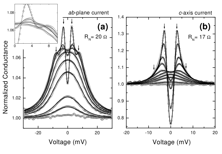
Figure 1 shows the temperature dependence of the experimental normalized conductance curves (circles) of point contacts obtained by using an Ag-paint spot (a) and an In flake (b). The values of the normal-state resistance (independent of the temperature) are indicated in each panel. In (a) the current was mainly injected along the planes, while in (b) the current direction was mainly parallel to the axis. The low-temperature curves in (a) clearly show two peaks at mV and mV, that merge in a broad maximum above 15 K. The low-temperature curves in (b), instead, show only a very sharp peak at mV and a smooth shoulder at mV. Clearly, these features are connected to the two gaps and , and the different relative amplitude of the peaks reflects the angular dependence of the weight of each band in the total conductance. In the panels of Figure 1, solid lines are the best-fitting curves calculated by using the BTK model [10] generalized to the case of two gaps. In other words, the experimental normalized conductance was fitted to a function of the form: . The fit is almost perfect especially at low voltage. This might not surprise since there are 7 adjustable parameters: and , the broadening parameters and , the barrier transparency coefficients and , and the weight of the band in the total conductance, . Actually, since neither the current direction nor the contact resistance depend on the temperature, both and the barrier parameters and were kept equal to their low- values.
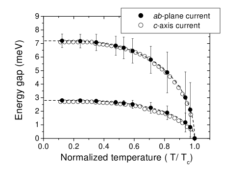
Figure 2 reports the temperature dependence of the two gaps given by the fit, both for -plane current (solid circles) and for -axis current (open circles). The low-temperature gap values meV and meV agree very well with the theoretical values [3] but are larger than those measured by specific heat [12] and thermal conductivity [13] in similar samples 111A possible reason is that the theoretical gap values were calculated by starting from the resistive (i.e., 39 K), while the bulk seems to be lower [14]. This might indicate that surface effects play a role in MgB2, affecting surface-sensitive measurements such as point-contact spectroscopy.. Unfortunately, at higher temperature the error on the gap values increases so much that it becomes practically impossible to determine whether the and curves follow a BCS-like curve or not. Let us also mention that the values of the parameter resulting from the fit are in the case of -plane current and in the case of -axis current. The values predicted by the two-band model are and for current injection purely along the plane and along the axis, respectively [3]. Since the crystal orientation is known with a few degrees of accuracy, this apparent mismatch is actually due to the fact that, in point-contact spectroscopy, the current injection occurs within a finite solid angle [8].
A careful test of the two-band model obviously requires a more accurate determination of the gap amplitude. This might be obtained by reducing the number of free fitting parameters, e.g. by separating the contributions of the two bands to the total conductance. Some results obtained in polycrystalline samples [5], suggest that a magnetic field of suitable intensity (namely, about 1 T at 4.2 K) can remove the gap in the bands without affecting the gap in the bands. We verified that the same happens in our single crystals: we applied to each sample (at K) magnetic fields of increasing intensity, either parallel to the axis or to the planes, and we observed that in both cases the small-gap features in the conductance curves vanish indeed when T [11]. The effect of the field on the large gap depends instead on the field direction. When -plane, the large-gap features remain clearly distinguishable up to 9 T, with only some marks of gap closing. Incidentally, this demonstrates that T. When -axis, instead, the conductance peaks due to the large gap merge together at T giving rise to a broad maximum. Based on the high value of at low temperature (suggested both by our measurements and by other results on similar samples [14, 15]), and supported by some measurements at various temperatures [16], we assumed that a field of 1 T parallel to the planes was too weak to affect seriously the large gap, even at temperatures rather close to .
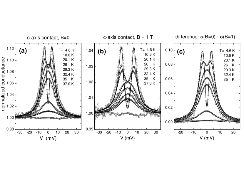
Then, we measured the conductance curves of a In-MgB2 point-contact in the -axis-current case as a function of the temperature, with no field (see Figure 3a) and with a field of 1 T parallel to the planes (see Figure 3b). If in the absence of magnetic field the total normalized conductance reads , when the magnetic field destroys the gap in the band it becomes: . Thus we fitted the curves measured in the presence of the field with this function, that only contains three free parameters: , and . We took , that is the value obtained from the fit of the total conductance at low temperature. Incidentally, the good quality of the fit (solid lines in Figure 3) shows that the value we got for is a very good evaluation, and that the field completely suppresses the small gap. The temperature dependence of obtained from this fitting procedure is reported in Figure 4 (open circles).
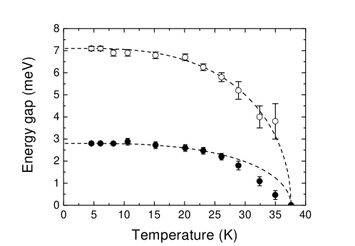
A comparison with Figure 2 clearly shows the reduction of the error bars and hence the improvement of the accuracy obtained by using this novel technique. Also notice that follows rather well a BCS-like curve, as in Figure 2. The absence of any field-induced suppression of proves a posteriori that a field of 1 Tesla parallel to the plane has a negligible influence on the band, even at temperatures rather close to .
An independent determination of the small gap can be obtained by subtracting the conductance curve measured in the presence of the field (Figure 3b) from those measured without field (Figure 3a). The resulting curves are reported in Figure 3c. Notice that these curves look particularly “clean” and noise-free since the subtraction also allows eliminating some experimental fluctuations that are present both in and in . The result of the subtraction can be expressed by the functional form . Fitting the experimental data with this function allows determining the three remaining free parameters , and . The resulting temperature dependence of the small gap is reported in Figure 4 (solid circles). In this case, the error on the gap value is very small even at high temperature, so that the deviation of the gap values from the BCS-like curve (dashed line) results to be much larger than the experimental uncertainty.
4 Conclusions
The selective removal of the gap in the bands from the total conductance curves of point contacts is by itself a proof of the existence of two distinct gaps in MgB2. In this paper we have shown that the use of single crystals allows a stricter test of the two-band model. First, the fit of the total conductance curves with the generalized BTK model gave us the weights of the and bands, which resulted in good agreement with those predicted theoretically both for contacts along the axis and along the planes. Second, the separate analysis of the partial conductances and gave the highest-precision values of the gaps in MgB2 ever obtained by point-contact spectroscopy: at low , meV and meV. While follows a BCS-like temperature evolution, deviates from the BCS behaviour at K, in very good agreement with the two-band model. Due to the small error on the gap value, this deviation is here unquestionably determined for the first time.
This work was supported by the INFM Project PRA-UMBRA and by the INTAS project “Charge transport in metal-diboride thin films and heterostructures”.
References
References
- [1] Kortus J, Mazin I I, Belashchenko K D, Antropov V P and Boyer L L, 2001 Phys. Rev. Lett. 86 4656; Shulga S V, Drechsler S -L, Eschrig H, Rosner H and Pickett W E cond-mat/0103154; An J M and Pickett W E 2001 Phys. Rev. Lett. 86 4366; Kong Y, Dolgov O V, Jepsen O and Andersen O K 2001 Phys. Rev. B 64 020501(R).
- [2] Liu A Y, Mazin I I and Kortus J 2001 Phys. Rev. Lett. 87 87005.
- [3] Brinkman A, Golubov A A, Rogalla H, Dolgov O V, Kortus J, Kong Y, Jepsen O and Andersen O K 2001 Phys. Rev. B 65 180517(R).
- [4] Giubileo F, Roditchev D, Sacks W, Lamy R, Thanh D X, Klein J, Miraglia S, Fruchart D, Marcus J and Monod P 2001 Phys. Rev. Lett. 87 177008; Iavarone M, Karapetrov G, Koshelev A E, Kwok W K, Crabtree G W and Hinks D G cond-mat/0203329; Martinez-Samper P, Rodrigo J G, Rubio-Bollinger G, Suderow H, Vieira S, Lee S and Tajima S cond-mat/0209387; Eskildsen M R, Kugler M, Levy G, Tanaka S, Jun J, Kazakov S M, Karpinski J and Fischer Ø cond-mat/0209345.
- [5] Szabó P, Samely P, Kačmarčík J, Klein T, Marcus J, Fruchart D, Miraglia S, Marcenat C and Jansen A G M 2001 Phys. Rev. Lett. 87 137005-1.
- [6] Suhl H, Matthias B T and Walker L R 1959 Phys. Rev. Lett. 3 552.
- [7] For further details, see the relevant paper in the Proceedings of this Conference and ref. [15].
- [8] Kashiwaya S and Tanaka Y 2000 Rep. Prog. Phys. 63 1641.
- [9] Jansen A G M, van Gelder A P and Wyder P 1980 J. Phys. C: Solid St. Phys. 13 6073; Duif A M, Jansen A G M and Wyder P 1989 J. Phys.: Condens. Matter 1, 3157.
- [10] Blonder G E, Tinkham M and Klapwijk T M 1982 Phys. Rev. B 25 4515.
- [11] Gonnelli R S, Daghero D, Ummarino G A, Stepanov V A, Jun J, Kazakov S M and Karpinski J cond-mat/0208060.
- [12] Bouquet F, Wang Y, Sheikin I, Plackowski T, Junod A, Lee S and Tajima S cond-mat/0207141.
- [13] Sologubenko A V, Jun J, Kazakov S M, Karpinski J and Ott H R cond-mat/0111273.
- [14] Sologubenko A V, Jun J, Kazakov S M, Karpinski J and Ott H R 2002 Phys. Rev. B 65 180505(R).
- [15] Angst M, Puzniac R, Wisniewski A, Jun J, Kazakov S M, Karpinski J, Roos J and Keller H 2002 Phys. Rev. Lett. 88 167004.
- [16] Gonnelli R S, Daghero D, Ummarino G A, Stepanov V A, Jun J, Kazakov S M and Karpinski J cond-mat/0209516.