Temperature induced shift in the pinch-off voltage of mesoscopic devices
Abstract
Detailed experimental studies of the conductance of mesoscopic GaAs devices in the few-mode regime reveal a novel thermal effect: for temperatures up to at least 10 K the measured gate characteristics, i.e. conductance versus gate voltage , exhibit a systematic downward shift in gate voltage with increasing temperature. The effect is ’universal’, in the sense that it is observed in different modulation doped GaAs/GaAlAs heterostructures, in different device geometries, and using different measurement setups. Our observations indicate that the effect originates in the surrounding 2D electron gas and not in the mesoscopic devices themselves.
pacs:
73.61.-r, 73.23.-b, 73.23.AdI Introduction
In numerous studies of ballistic mesoscopic devices reported in the literature the main effect of increasing the temperature is thermal smearing smearing of the conductance traces as becomes comparable with the characteristic intrinsic energy scale of the device. This is also the main effect in the six sets of gate characteristics (conductance versus gate voltage ) in Fig. 1 taken from our own experiments Kristensen2000 ; Hansen2001 on GaAs quantum point contacts (QPC), quantum wires (QW), and Aharonov-Bohm (AB) rings.

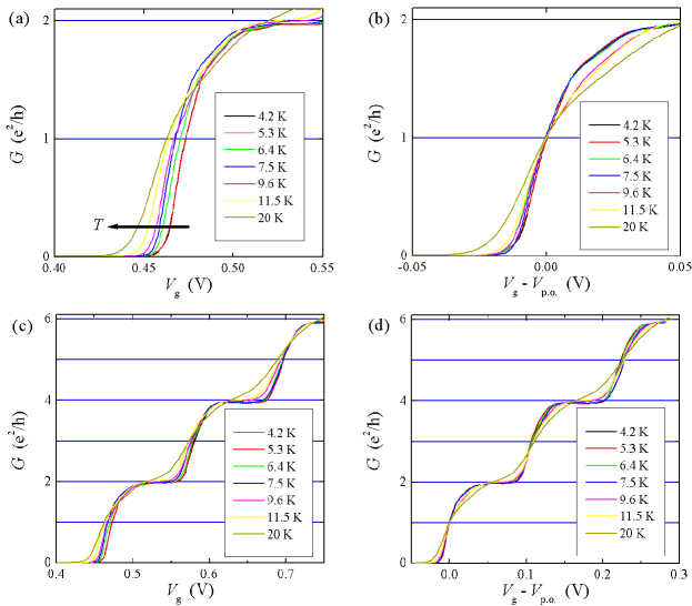
On closer inspection we also observe that the gate characteristics always exhibit a systematic downward shift in gate voltage with increasing temperature. We observe this shift in all our shallow-etched mesoscopic devices independent of the sample geometry and of the measurement set-up. This observation is the main topic of this paper, and to our knowledge it has not been reported in the literature before. The effect may easily be masked by thermal smearing of the conductance traces, so to study it in detail it is important to make the intrinsic energy scale as large as possible. As in our previous work Kristensen2000 , we achieve this by relying on a shallow-etch technique in the fabrication of the mesoscopic devices. This technique yields particularly strong lateral confinement allowing for well quantized conductances up to 10 K. The shift of the conductances traces is most clearly seen in Figs. 1a and 1b, which are QPCs with large subband-spacings, above 10 meV. Hence, these samples are chosen for the detailed analysis in the following sections.
II Shallow etched mesocopic devices
Our devices were fabricated on modulation doped GaAs/GaAlAs heterostructures with a 2-dimensional electron gas (2DEG) buried 90 nm below the surface. Typical 2DEG mobilities and densities are 60–100 m2V-1s-1 and 1.5 – 31015 m-2, respectively. The samples were processed with a wide and long Hall bar mesa fitted with ohmic Au/Ge/Ni contacts to the 2DEG. The mesoscopic devices were defined on top of the mesas by electron beam lithography and an approximately 30 nm deep wet shallow-etch. The electron densities are controlled by gate-electrodes in the form of either Cr/Au top-gate electrodes, deposited on top of the mesoscopic devices, or by in-plane side-gate electrodes using the 2DEG outside the shallow etched trenches. For details of the samples and the sample fabrication, we refer to Ref. Kristensen2000, .
Scanning electron microscope (SEM) pictures of some of our shallow etched mesoscopic devices are shown as insets in Fig. 1. The two devices in Figs. 1a and 1b are QPCs, the two devices in Figs. 1c and 1d are QWs, and the last two devices in Figs. 1e and 1f are AB rings. The QWs are controlled by side-gate electrodes, while the QPCs and the AB rings were fitted with top-gate electrodes after the SEM pictures were taken. The electrically insulating, shallow-etched regions appear dark on the pictures. The mesoscopic devices are normally pinched-off, and positive gate voltage is applied to open for electron transport as seen on Fig. 1. The gate electrode leakage current was always negligible (less than 100 pA) in the data presented here.
The QPCs in Figs. 1a and 1b, henceforth denoted device A and B, are studied in detail in the following sections. They are fabricated from the same GaAs/AlGaAs heterostructure, with a 2DEG having the density m-2 and the mobility 80 m2/Vs. The two QPCs have etched widths of 70 nm and 150 nm, respectively. On both devices, a wide Cr/Au top-gate electrode covers the etched constriction and the neighboring 2DEG. The devices were characterized by finite source-drain bias spectroscopy Patel91 , and we found an energy spacing between the first two subbands of 14 meV and 10 meV, respectively.
The data from sample A and B presented here, were recorded by immersing the sample into a liquid helium container. Temperatures above K were obtained with the sample placed at different heights in the helium vapor above the liquid. The differential conductance was measured in a four-terminal voltage controlled setup, using a standard lock-in technique at 117 Hz. Here is the source-drain voltage bias and the corresponding current. The rms amplitude of the applied was , selected to be much smaller than to ensure linear response. The dc-component of was zero with a precision of a few .
Our four-terminal measurement setup eliminates most of the series resistance from the surrounding 2DEG except for a small residual. To study the thermally induced translation of the conductance traces it is not necessary to correct for the residual series resistance. However, following the procedure described in Ref. Hansen2002, it is easy to do so, and in fact it was done with the data from sample A in the following analysis.

III Conductance and pinch-off
In Fig. 2 we have replotted the conductance data from Fig. 1a, i.e. from sample A. Fig. 2a contains a zoom-in on the first conductance step. It is apparent from this plot that the conductance traces below for the lowest temperatures have almost identical shapes. The inevitable thermal smearing is only significant for the highest temperature in the plot, K. It seems that the conductance traces are translated towards lower gate voltages as temperature is increased. This hypothesis is tested successfully in Fig. 2b, where the conductance traces have been shifted horizontally along the gate voltage axis to coincide at the conductance value . All the curves (except the K curve) fall nearly on the same trace for . The temperature dependence of the conductance is different for due to the so-called 0.7 structure Thomas , an effect we do not study in this work.
We choose the value as the anchor point in the translation of the conductance traces for two reasons. Firstly, in the simplest single-particle models of QPC-conductance this point remains fixed when temperature is raised until the quantized conductance is destroyed, i.e., for temperatures smaller than subband spacing ()Buttiker1990 . Secondly, it is natural to define the ’pinch-off’ voltage at a given temperature as the gate voltage at which the chemical potential of the reservoirs aligns with the subband edge of the first 1D subband and the conductance acquires half its full plateau value, i.e. . The translation we perform is thus achieved by replacing with .
In Figs. 2c and 2d we examine the shift in pinch-off voltage for the higher conductance plateaus. Panel (c) and (d) show the data before and after translation, respectively. On Fig. 2d we observe that the translation have turned not only into a fix point but also to a good approximation , as predicted by the simple QPC-models Buttiker1990 .
To summarize, our data analysis of Fig. 2 reveals that in addition to smearing, an increased temperature also gives rise to a systematic downward shift of the conductance traces towards lower gate voltage. The same conclusion is reached when analyzing other samples, including the ones shown in Fig. 1.
IV The shift in pinch-off voltage
To study the pinch-off voltage shift in more detail, we show in Fig. 3 data from sample A (top row panels) and sample B (bottom row panels).
In the left column, panels (a) and (d), we have plotted the measured pinch-off voltage versus temperature as filled circles. For sample A in panel (a) the open circles show the ’pinch-off’ voltage for the second conductance step defined by using instead of . These data points have been shifted by mV to fit in the figure. We note that all three data sets show an apparent linear downward shift of the pinch-off voltage with increasing temperature. The solid lines represent linear fits to the three data sets, and we find nearly identical slopes , namely mV/K for sample A first step, mV/K for sample A second step, and mV/K for sample B first step. The nearly identical and gives quantitative support for our claim (see Fig. 2) that the shift in pinch-off voltage is in fact a shift of the entire conductance trace. More remarkable is the nearly identical and , i.e. two differently designed devices from the same heterostructure exhibit the same shift. This leads to the idea that the temperature induced shift in the pinch-off voltage is caused by the 2DEG surrounding the mesoscopic device rather than by the device itself.
The middle and right columns in Fig. 3 are shown to document our measurement procedure, and to illustrate that the indeed quite small shift in pinch-off voltage is significant and reproducible.
The middle column, panel (b) and (e), show the order in which the data in panel (a) and (d) have been recorded. For each data point the corresponding temperature in kelvin is indicated. Each sequence was recorded over several hours to ensure proper thermal equilibrium at the different temperatures. In order to exclude device instabilities as an explanation for the observed shifts in pinch-off voltage, measurements at base temperature 4.2 K were repeated. The 4.2 K data in panels (b) and (e) verify the stability of the devices.
In the right column, panel (c) and (f), the solid lines are plots of the whole conductance trace for all base temperature measurements of panel (b) and (e). These plots show a negligible temporal drift of the entire conductance trace. The dashed lines in panel (c) and (f) are conductance traces recorded at high temperature. From the plots we see that the temperature induced shift of a few mV is significant compared to the temporal drift.
V Suppression of thermal smearing
For conductances in the range there is a tendency to suppression of thermal smearing. While this effect is not central to the shift in pinch-off voltage, it is very useful in establishing the very existence of this shift, as demonstrated clearly in Fig. 2.
There are several possible explanations for the suppression of thermal smearing. One is the tunnelling effect through the QPC barrier. For example, in the quadratic saddle point approximation the transmission at zero temperature is described by a Fermi-function with an effective temperature . For temperatures less than the shape of the conductance trace is roughly independent of temperature and thermal smearing only becomes significant for .Buttiker1990
Another explanation involves Coulomb interaction between electrons. This interaction gives rise to an energy scale that suppresses the thermal smearing for . This effect may be seen in the simulations presented in Ref. Hirose, .
VI Discussion
We have presented detailed experimental studies of the conductance of mesoscopic devices in the few-mode regime. Our data show a novel thermal effect: for temperatures up to at least 10 K the measured conductance traces are systematically shifted downwards in gate voltage as the temperature is raised. This shift is ’universal’: it is always observed in our shallow-etched mesoscopic devices independent of sample geometry and measurement set-up. This apparent ’universality’ of the shift leads to the idea that the effect originates in the physics of the surrounding 2D electron gas and not in the physics of the mesoscopic device itself. The observation that different devices from the same wafer exhibits nearly the same shift lends further support to this idea.
The data presented here are far from sufficient to draw final conclusions regarding the underlying physics of the temperature shift. We can rule out non-interacting models. Although these models are capable of producing a thermally induced change of the anchor point by allowing for transmission functions with non-trivial energy dependencies, such changes are induced by, and cannot therefore be separated from, thermal smearing. This is in contrast to the experimental observations. It may therefore be interesting to consider interaction effects, e.g., the following possibilities.
The almost pure translation of the conductance traces could most simply be explained in terms of a temperature dependent shift in the chemical potential of the surrounding 2DEG. Within the Landauer-Büttiker formalism such a shift measured relative to the transmission barrier of the mesoscopic device would directly lead to a translation of the conductance trace, since the temperature would then play a role similar to a conventional density-controlling gate electrode. The observed downward shift of the conductance traces would arise if the chemical potential of the 2DEG rises with increasing temperature. Such a rise could be due to a gradual reduction of the exchange and correlation energy in the 2DEG.
Another possible explanation could be based on a Coulomb-interaction induced shift of the subband edge in the mesoscopic device Hirose combined with the existence of a threshold density controlling the onset of electron transmission. In this case, an increase in temperature widens the derivative of the Fermi-distribution, which controls the conductance. The high-energy tail will then reach the subband edge for a lower chemical potential. Consequently, the threshold density is reached for lower chemical potential, i.e. for lower gate voltage, as the temperature is raised.
We would like to emphasize that the ’universality’ of the observed temperature induced shift of the pinch-off voltage means that the samples shown here are not in any way unique, they simply represent the samples where the temperature dependence has been checked most thoroughly by the procedure shown in Fig. 3.
Acknowledgements
We thank C.B. Sørensen for growing the semiconductor structures. This work was partly supported by the Danish Technical Research Council (grant no. 9701490) and by the Danish Natural Science Research Council (grants no. 9502937, 9600548 and 9601677). The III-V materials used in this investigation were made at the III-V NANOLAB, operated jointly by Research Center COM, Technical University of Denmark, and the Niels Bohr Institute, University of Copenhagen.
References
- (1) The thermal smearing is spawned by decoherence processes and statistical distribution functions.
- (2) A. Kristensen, H. Bruus, A.E. Hansen, J.B. Jensen, P.E. Lindelof, C.J. Marckmann, J. Nygård, C.B. Sørensen, F. Beuscher, A. Forchel, M. Michel, Phys. Rev. B 62, 10950 (2000).
- (3) A.E. Hansen, A. Kristensen, S. Pedersen, C.B. Sørensen, and P.E. Lindelof, Phys. Rev. B. 64, 45327 (2001)
- (4) N.K. Patel, J.T. Nicholls, L. Martin-Moreno, M. Pepper, J.E.F. Frost, D.A. Ritchie, and G.A.C. Jones, Phys. Rev. B 44, 13549 (1991)
- (5) A.E. Hansen, A. Kristensen, H. Bruus, Proc. ICPS-26 (2002), cond-mat/0208452.
- (6) K.J. Thomas, J.T. Nicholls, M.Y. Simmons, M. Pepper, D.R. Mace, and D.A. Ritchie, Phys. Rev. Lett. 77, 135 (1996).
- (7) M. Büttiker, Phys. Rev. B 41, 7906 (1990).
- (8) K. Hirose and N.S. Wingreen, Phys. Rev. B 64, 073305 (2001)