Observation of vortex structure in MgB2 single crystals by Bitter decoration technique
Abstract
We report the observation of superconducting vortices in pure and lightly Al doped MgB2 single crystals. Low field experiments allow for the estimation of the London penetration depth, lambda 1900 for T6 K. Experiments in higher fields (e.g. 200 Oe) clearly show a triangular vortex lattice in both real space (13 m by 13 m Bitter decoration image of over 1000 vortices) and reciprocal space.
pacs:
74.60.Ge, 74.70.AdThe recent discovery of superconductivity with 39 K in the simple intermetallic compound, magnesium diboride, Jap has caused an explosion of experimental and theoretical works with a major part of the measurements being performed on polycrystalline samples. P1 ; P2 ; P3 ; P4 ; P5 Until now only a few groups have been able to grow (small, sub-mm size) single crystals of MgB2. X1 ; X2 ; X3 ; X4 From the very earliest data P2 it became clear that MgB2 is a type-II superconductor with its electromagnetic properties described within the framework of the vortex state. AAA So far, for the most part, bulk techniques (magnetization, magneto-transport, etc.) that evaluate the ”average” properties of the sample were used for studies of the superconducting state of MgB2. On the other hand, direct imaging of the vortices is more of a local probe that can evaluate the homogeneity and strength of pinning for different parts of the sample. In addition this technique allows for the determination of basic superconducting properties such as anisotropy and London penetration depth .
In this work we use one of the direct techniques for the imaging of vortices: high resolution Bitter decoration, a technique that allows for the observation of the individual vortices (in small applied magnetic field) as well as for the imaging of vortex structures in a wide range of magnetic fields (up to 2kOe PRBLu ). It should be emphasized, though, that this technique requires that the surface of the sample be very clean and optically smooth. To achieve this degree of surface perfection, single crystals have to be used.
The single crystals used for our decoration experiments were grown using a high pressure cubic anvil technique from a mixture of Mg and B in a BN container (see X4 ; X5 for details). The samples used for decoration were plates with the approximate dimensions . In addition to pure MgB2 single crystals ( K, K), crystals of nominal composition Mg0.99Al0.01B2 and Mg0.98Al0.02B2 (both with K, K) were studied. The decoration was performed in the field-cooled (frozen flux) regime in applied magnetic fields () from several Oersted to 200 Oe. The temperature of the sample before the decoration was either 1.4 K or 4.2 K, during the decoration process the temperature increased several degrees; up to 4-5 K or 6-8 K respectively by the end of the decoration process. The vortex structures were observed on the as grown surfaces of the crystals using field emission scanning electron microscope in the secondary electron emission regime to locate the small islands of iron.
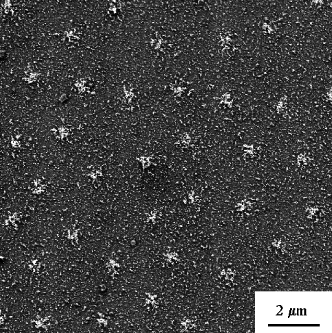
Figure 1 shows the structure of vortices in MgB2 for a small applied magnetic field ( G). The observed structure is a collection of weakly interacting individual vortices that do not form a regular triangular lattice (and do not have long range order). The diameter, d, of the image of a single vortex (”vortex diameter”) is, on average, 0.770.2 m, a value that is much less than the distance between vortices. Taking into account the vortex expansion Pearl near the surface of a superconductor, the London penetration depth can be estimated as with lambda that results in for the temperature of the decoration experiment 6K. Common techniques for the measurements of London penetration depth in superconductors usually give very precise relative changes of as a function of temperature and/or applied magnetic field. At the same time the accuracy in the absolute value of is usually around several tens-of-percents. Since the range of the experimental values of the penetration depth for MgB2 obtained using different techniques is rather wide ( blah5 ; 5a ; 5b ; 5c ) our estimate of from the size of the vortex image is useful by virtue of giving a reliable absolute value to the upper limit of the penetration depth. Several issues should be remembered in the course of such estimate. It is important to have the density of magnetic particles high enough to fill the region of the magnetic flux penetration in the vicinity of the vortex. From Fig. 1 it is clear that this condition is satisfied since the magnetic particles are observed in the area between the vortices. The correct estimate of the value of the coefficient that accounts for the vortex expansion near the surface of a superconductor is apparently the main source of uncertainty in our estimate of . Empirically, a comparison between the values for the penetration depth from decoration experiments and those obtained by other techniques in different materials where the values of are considered to be reliable (Nb, , NbSe2) vin1 ; vin2 give the upper limit of errors in from Bitter decoration of using .
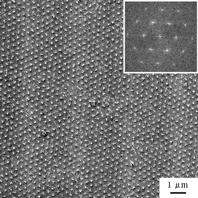
In higher applied magnetic fields a regular triangular lattice is clearly observed (see Fig. 2). No difference in vortex structure was seen between pure and Al-doped MgB2 crystals. Fig. 2 shows the vortex lattice for MgB2 single crystal in 200 Oe applied field. The remarkably high quality of the vortex lattice can be seen in the real-space image as well as from the fast Fourier transform (FFT) pattern (inset fig.2). Autocorrelation function allows to estimate the translational length as 8-9 intervortex spacings. Our observation of the hexagonal vortex lattice is in a good agreement with the imaging of vortex unit cell by STM at the magnetic fields of 2kG X6 as well as 5 kGs. X5 It is worth noting that, given the high degree of order shown by the flux line lattice in Fig. 2, MgB2 should prove to be an excellent system for small angle neutron scattering (SANS) measurements.
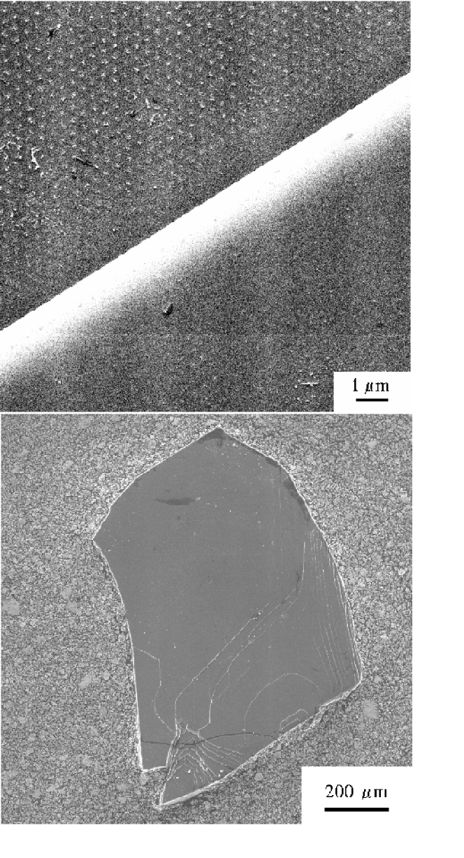
In pure and doped magnesium diboride single crystals Meissner rims (narrow regions free from vortices) were often observed (see Fig. 3) near the top of growth steps and crystal edges. In the latter case the width of the stripe was several tens of microns that is comparable with the thickness of the crystals. Meissner rims were observed in several other superconductors blah ; blah1 ; blah2 with weak volume pinning in which case interaction of vortices with the lateral surface of the crystal becomes significant. The observation of a regular triangular lattice and Meissner rims in pure and Al-doped magnesium diboride single crystals point to weak volume pinning and therefore to high quality, with regards to pinning, of the crystals used in the decoration experiments.
As part of our search for effects caused by the expected anisotropy of the London penetration depth blah3 we made several attempts to perform Bitter decoration experiments in a tilted magnetic field using the same single crystals that were utilized for measurements shown above (after cleaning the samples from magnetic particles). However imperfections of the observed vortex structure (smeared maxima in the FFT pattern) did not allow us to reach any unambiguous conclusions about the anisotropy of . These imperfections could be caused, at least in part, by possible damage of the surface of the crystals during the cleaning process. Decoration experiments in tilted and perpendicular to magnetic field will be part of the future studies and still do have the potential of addressing important issues of superconducting anisotropies in MgB2.
In summary, a clear triangular vortex lattice was observed in an applied field of Oe () for Mg1-xAlxB2 single crystals ( = 0, 0.01, 0.02) by Bitter decoration technique. The Meissner rims seen near the growth steps and crystal edges suggest very small volume pinning in these crystals. And an upper limit of the London penetration depth at T 6 K was estimated from decoration experiments in very low fields.
Acknowledgements.
We wish to thank V.G. Kogan for useful discussions. Ames Laboratory is operated for the U. S. Department of Energy by Iowa State University under Contract No. W-7405-Eng.-82. This work was supported by the director for Energy Research, Office of Basic Energy Sciences. Partial support by NATO Collaborative Linkage Grant #PST.CLG.978513 is acknowledged. L.Ya.V. was partially supported by RFBR 00-02-04019a grant and Minestry of Industry,Science and Technologies grant 40.012.1.1.11.46 (Russia).References
- (1) J. Nagamatsu, N. Nakagawa, T. Muranaka, Y. Zenitani and J. Akimitsu, Nature 410, 63 (2001)
- (2) S. L. Bud’ko, G. Lapertot, C. Petrovic, C. E. Cunningham, N. Anderson, and P. C. Canfield, Phys. Rev. Lett. 86, 1877 (2001)
- (3) D. K. Finnemore, J. E. Ostenson, S. L. Bud’ko, G. Lapertot, and P. C. Canfield, Phys. Rev. Lett. 86, 2420 (2001)
- (4) P. C. Canfield, D. K. Finnemore, S. L. Bud’ko, J. E. Ostenson, G. Lapertot, C. E. Cunningham, and C. Petrovic, Phys. Rev. Lett. 86, 2423 (2001)
- (5) F. Bouquet, R. A. Fisher, N. E. Phillips, D. G. Hinks, and J. D. Jeogensen, Phys. Rev. Lett. 87, 047001 (2001)
- (6) D. C. Larbalestier et al, Nature 410, 186 (2001)
- (7) M. Xu, H. Kitazawa, Y. Takano, K. Nishida, H. Abe, A. Matsushita, N. Tsujii and G. Kido, Appl. Phys. Lett. 79, 2779 (2001)
- (8) S. Lee, H. Mori, T. Masui, Yu. Eltsev, A. Yamamoto and S. Tajima, J. Phys. Soc. Jpn. 70, 2255 (2001)
- (9) K. H. P. Kim, J. H. Choi, C. U. Jung, P. Chowdhury, H. S. Lee, M. S. Park, H. J. Kim, J. Y. Kim, Z. Du, E. M. Choi, M7. S. Kim, W. N. Kang, S. I. Lee, G. Y. Sung and J. Y. Lee, Phys. Rev. B 65, 100510 (2002)
- (10) M. Angst, R. Puzniak, A. Wisniewski, J. Jun, S. M. Kazakov, J. Karpinski, J. Roos and H. Keller, Phys. Rev. Lett. 88, 167004 (2002)
- (11) A. A. Abrikosov, Zh. Eksp. Teor. Fiz. 32, 1442 (1957)
- (12) L. Ya. Vinnikov, T. L. Barkov, P. C. Canfield, S. L. Bud’ko, J. E. Ostenson, F. D. Laabs and V. G. Kogan, Phys. Rev. B 64, 220508 (2001)
- (13) J. Karpinski, M. Angst, J. Jun, S. M. Kazakov, R. Puzniak, A. Wisniewski, J. Roos, H. Keller, A. Perucchi, L. Degiorgi, M. Eskildsen, P. Bordet, L. Vinnikov and Mironov, cond-mat 0207263 (2002)
- (14) J. Pearl, J. Appl. Phys. 37, 4139 (1966)
- (15) M. Indenbom, private communication
- (16) Yu. Nefyodov, M. R. Trunin, A. F. Shevchun, D. V. Shovkun, N. N. Kolesnikov, M. P. Kulakov, A. Aglio Gallitto and S. Fricano, Europhys. Letters. 58, 422 (2002)
- (17) M. Zehetmayer, M. Eisterer, J. Jun, S. M. Kazakov, J. Karpinski, A. Wisniewski and H. W. Weber, Phys. Rev. B 66, 052505 (2002)
- (18) C. Buzea and T. Yamashita, Supercond. Sci. Technol. 14, R115 (2001)
- (19) L. Ya. Vinnikov , L. A. Gurevich, G. A. Emelchenko and Yu. A. Osipyan, Solid State Commun. 67 , 421 (1988).
- (20) R. E. Schwall, G. R. Stewart and T. H. Gebale, J. Low. Temp. Phys. 22, 557 (1976)
- (21) R. A. Kaindl, M. Acatnahan, J. Orenstein, D. S. Chermla, H. M. Christen, H. -Y. Zhai, M. Paranthamanand and D. H. Lowndes, cond-mat 0106342 (2001)
- (22) H. Dai, J. Liu and C. M. Lieber, Phys. Rev. Lett. 72, 748 (1994)
- (23) F. Pardo, F. de la Cruz, P. L. Gammel, E. Bucher, C. Ogelsby and D. J. Bishop, Phys. Rev. Lett. 79, 1369 (1997)
- (24) L. Ya. Vinnikov, T. L. Barkov, B. Irmer, K. Kragler and G. Saemann - Ischenko, Physica C 308, 99 (1998)
- (25) V. G. Kogan, Phys. Rev. B 66, 020509 (2002)
- (26) M. Eskildsen, M. Kugler, S. Tanaka, J. Jun, S. M. Kazakov, J. Karpinski, and O. Fischer, cond-mat 0207394 (2002)