Low frequency noise in doped manganite grain-boundary junctions
Abstract
We have performed a systematic analysis of the low frequency -noise in single grain boundary junctions in the colossal magnetoresistance material . The grain boundary junctions were formed in epitaxial films deposited on bicrystal substrates and show a large tunneling magnetoresistance of up to 300% at 4.2 K as well as ideal, rectangular shaped resistance versus applied magnetic field curves. Below the Curie temperature the measured noise is dominated by the grain boundary. The dependence of the noise on bias current, temperature and applied magnetic field gives clear evidence that the large amount of low frequency noise is caused by localized sites with fluctuating magnetic moments in a heavily disordered grain boundary region. At 4.2 K additional temporally unstable Lorentzian components show up in the noise spectra that are most likely caused by fluctuating clusters of interacting magnetic moments. Noise due to fluctuating domains in the junction electrodes is found to play no significant role.
pacs:
75.30.Vn, 73.50.Td, 72.70.+mI Introduction
Doped manganites have attained large interest in recent years because of the interesting interplay of charge, spin, orbital and structural degrees of freedom in these materials Salamon01 and their potential use in magnetoresistive devices. It was found early that the introduction of artificial grain boundaries (GB) into epitaxial manganite thin films leads to localized structural distortions at the GB entailing significant modifications of the magnetotransport properties of the GB Gubkin93a ; Hwang96 ; Gupta96 ; Mathur97 ; Steenbeck97 ; Klein99a ; Gross99a ; Hoefener00 ; Ziese99a . In particular, a significant increase of the low field magnetoresistance was found. Recently, in well-defined, individual GB junctions fabricated by depositing epitaxial manganite films on bicrystal substrates, a large two-level magnetoresistance effect with a maximum tunneling magnetoresistance (TMR) of up to 300% at 4.2 K has been demonstrated at low applied fields of about 200 Oe Hoefener00 ; Philipp00 . These artificial GB junctions showed an almost ideal two-level resistance switching behavior with sharp transitions from the low to the high resistance state when the magnetic field was applied within the film plane parallel to the GB barrier. Thus, manganite GB junctions represent ferromagnetic (FM) tunnel junctions with very high TMR values and a very simple fabrication process. On the other hand, the charge transport mechanism across the GB barrier has not yet been unambiguously clarified. In well-defined bicrystal GB junctions defined by growing epitaxial manganite films on bicrystal substrates, the GB barrier is formed by a straight distorted GB interface with a width of only a few nm as shown by transmission electron microscopy Gross99a ; Gross00 ; Wiedenhorst00 . After annealing in oxygen atmosphere, individual GB junctions with large TMR values have been achieved Mathur97 ; Steenbeck97 ; Gross99a ; Hoefener00 ; Philipp00 .
Up to now, several theoretical models have been proposed Klein99a ; Gross99a ; Hoefener00 ; Ziese99a ; Evetts98a ; Coey98a ; Guinea98a to describe the magnetotransport properties of the manganite GB junctions. However, the proposed models are controversial and a thorough understanding of the magnetotransport properties of the GB junctions is still lacking what is mainly related to the unknown structural and magnetic properties of the GB barrier. Whereas Hwang et al. Hwang96 proposed a model based on spin-polarized tunneling between ferromagnetic grains through an insulating GB barrier, Evetts et al. Evetts98a proposed the polarization of the GB region by adjacent magnetically soft grains. Later on, Guinea Guinea98a pointed out that probably tunneling via paramagnetic impurity states in the GB barrier plays an important role and Ziese Ziese99a suggested a description of the transport characteristics of GB based on tunneling via magnetically ordered states in the barrier. Our recent systematic study of the magnetotransport properties of well-defined individual bicrystal GB junctions suggested a multi-step inelastic tunneling process via magnetic impurity states within a disordered GB barrier Klein99a ; Gross99a ; Hoefener00 ; Zhang98 . Within this model both the nonlinear current-voltage characteristics and the strong temperature and voltage dependence of the tunneling magnetoresistance could be naturally explained. In our model, strain and structural distortions at the GB interface result in a localization of charge carriers and thereby a suppression of the ferromagnetic double exchange resulting in an insulating GB barrier with a large density of magnetic impurity states. We also pointed out that band bending effects may play an important role resulting in a depletion layer at the GB interface below the Curie temperature of the ferromagnetic grain Gross99a .
Here, we report on a systematic analysis of the low frequency noise of individual bicrystal GB junctions to further clarify the transport mechanism across the GB interface. The investigation of the low frequency noise properties already has proven to be a valuable tool to provide more insight into transport mechanisms across grain boundaries in the structurally related cuprate superconductors Marx95a ; Marx99 ; Kemen99 . Therefore, the detailed evaluation of the noise of manganite GB junctions is highly desirable both from the basic physics and the application point of view.
For epitaxial thin films of the doped manganites there have been several reports on a large low frequency noise Alers96 ; Lisauskas99 ; Hardner97 ; Rajeswari96 ; Rajeswari98 . In particular, a large noise peak close to the Curie temperature has been interpreted in terms of a percolative nature of the transition between charge ordered insulating and ferromagnetic metallic states Podzorov00 ; Anane00 . However, Reutler et al. Reutler00 showed that the noise peak and the unusually large noise level is not an intrinsic property of the doped manganite. They found a strong coupling between local magnetic disorder and structural disorder introduced by strain effects due to lattice mismatch between film and substrate. In particular, the noise peak and the large noise level was found to be absent in high quality, strain free epitaxial films. Palanisami et al. Palanisami01 suggested two different mechanisms for the noise in manganite films: fluctuations between metallic and insulating phases on the one hand and magnetic orientation fluctuations (domain wall effects) on the other hand. Non-gaussian properties of the noise together with random telegraph signals were taken as an experimental hint to phase segregation in the colossal magnetoresistance (CMR) materials Raquet00 ; Merithew00 . On the other hand, random telegraph signals observed close to were taken as evidence for a domain-wall-motion picture of the kinetics of the responsible two-level system (TLS) Hess01 .
In contrast to epitaxial thin films there are almost no experimental data on the noise properties of grain boundaries in the doped manganites. Recently, Mathieu et al. investigated the zero-field low frequency noise in GB junctions in Mathieu01 below the ferromagnetic transition temperature as well as the magnetic field dependence of the noise. They concluded that the low-field noise was due to the multi-domain structure neighboring the GB i.e. of magnetic origin. Additional Lorentzian contributions were attributed to thermally activated domain wall motion in the domain configuration close to the GB.
In this article we present a systematic study of the low frequency noise in individual grain boundary junctions formed in films. In particular, we discuss the dependence of the measured noise on bias current, temperature and applied magnetic field. Our results show that below the noise is dominated by the GB and not by the adjacent grains. The analysis of the noise characteristics shows that the GB noise is due to localized states with fluctuating magnetic moments in a strongly disordered GB barrier. At the lowest temperatures ( K) additional Lorentzian contributions show up in the noise spectra. These Lorentzians are most likely due to an ensemble of interacting magnetic impurity states giving rise to a simultaneous switching of their magnetic moments.
II Sample preparation and experimental techniques
To achieve well-defined individual manganite grain boundary junctions (GBJs) first about 80 nm thick films were grown by pulsed laser deposition on symmetrical [001] tilt bicrystal substrates with a misorientation angle of 24∘. For details of the preparation process cf. Ref. Gross00 . The films typically had a Curie temperature K. After film deposition the films were annealed ex-situ at 950∘C in pure oxygen atmosphere. Then, typically 30 m wide microbrigdes straddling the grain boundary as well as the current and voltage leads are patterned into the biepitaxial films using optical lithography and Ar ion beam etching. For comparison, microbridges of the same spatial dimension that are not positioned across the grain boundary were patterned into the epitaxial film. A sketch of the sample geometry is shown in the inset of Fig. 1a. The GBJs fabricated in this way were characterized by measuring the current-voltage characteristics (IVCs) as a function of temperature and applied magnetic field. After the annealing process the GBJs show an almost perfect two-level resistance switching behavior with sharp transitions between the low and high resistance level as already has been reported recently Philipp00 .
The noise properties of the GBJs were measured by biasing the junctions at a constant current and measuring the low frequency voltage fluctuations superimposed on the resulting junction voltage. The voltage fluctuations were amplified by low-noise amplifiers and subsequently processed by a digital spectrum analyzer. In this way noise spectra have been taken in the frequency range from 1 Hz to 100 kHz. The measurements were performed as a function of temperature (4.2 to 300 K) and applied magnetic field (up to 12 T). The magnetic field always was applied within in the film plane parallel to the GB barrier. Great care has been taken of the electromagnetic shielding of the sample during the noise measurements.
In the following we will quantify the measured voltage noise power by the frequency independent normalized voltage noise power
| (1) |
Here, is the spectral density of the voltage fluctuations and the exponent usually is close to unity. Below, we will usually plot the octave integral
| (2) |
For we have .
III Experimental results and discussion
III.1 Transport and noise data
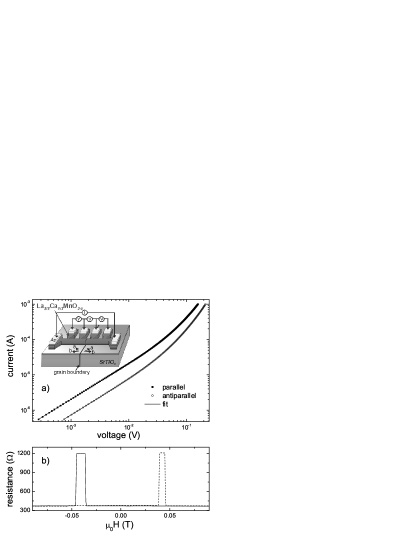
We first discuss the electrical transport properties of the GBJs. Typical current-voltage characteristics (IVCs) of a GBJ are shown in Fig. 1a. For the parallel magnetization direction in the electrodes the highly nonlinear IVCs can be accurately described within the Glazman-Matveev (GM) model Glazman88 for all temperatures below . Within the GM model the transport of charge carriers across a barrier containing a significant number of defect states is mediated both by elastic tunneling (direct or resonant tunneling via a single impurity state) and by inelastic tunneling processes via two and more defect states. Within this model the IVCs can be expressed by
| (3) |
where is the elastic contribution of direct and resonant tunneling via a single localized state and give the inelastic contribution to the total current from tunneling involving impurity states. The solid lines in Fig. 1a represent fits of Eq.(3) to the experimental data taking into account tunneling channels up to localized states Hoefener00 . Channels with are found to give only negligible contributions. For the antiparallel magnetization configuration the GM model also describes the IVCs at K amazingly well. We note, however, that for other temperatures the agreement with the GM prediction for the antiparallel configuration was not as perfect as shown in Fig. 1a.
In Fig. 1b we show the resistance versus applied magnetic field curve for the magnetic field applied within the film plane parallel to the grain boundary. As has been discussed in detail elsewhere Philipp00 , for this field direction the grain boundary junctions show an almost ideal rectangular shaped switching behavior between the low resistance state with parallel and the high resistance state with antiparallel magnetization orientation in the junction electrodes.
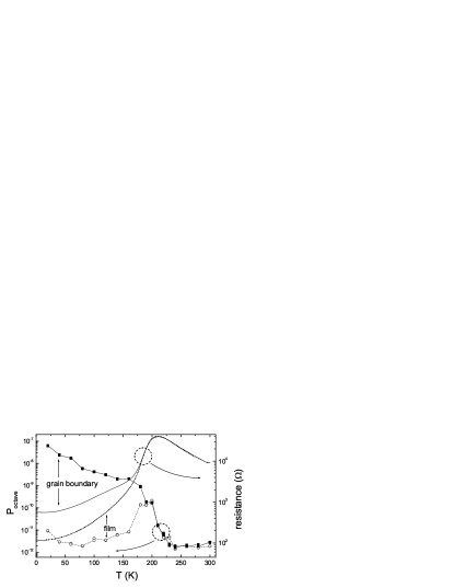
We next discuss the noise data. Figure 2 shows the temperature dependence of the normalized octave noise power for two microbrigdes of similar geometry. Whereas one microbridge is straddling the GB, i.e. contains an individual GBJ, the other is not positioned across the GB, i.e. does not contain a GBJ. By comparing the noise data of these two microbridges we can clearly identify the contribution of the GBJ to the measured noise. The noise for the microbridge with the GBJ is rapidly increasing with decreasing temperature for K. In contrast, the noise of the microbridge without GBJ is almost temperature independent except for a peak close to . We recently have shown that this noise peak can be suppressed by a small applied magnetic field and is related most likely to magnetic fluctuations at the paramagnetic to ferromagnetic transition in the doped manganites Reutler00 . The key result of Figure 2 is the fact that below the noise power of the microbridge with GBJ is orders of magnitude larger than the noise power of the epitaxial film. That is, for the microbridge with GBJ the measured noise can be attributed to the GBJ alone, since the additional noise of the adjacent grains is negligible small.
Although we do not want to discuss the details of the noise of the epitaxial film, we briefly compare the noise data of the epitaxial film shown in Figure 2 to those reported in our previous study Reutler00 . In Ref. Reutler00 we have analyzed the low frequency noise in highly strained films grown on SrTiO3 substrates. The magnitude of the noise measured for these strained films is much larger than that measured for the films of our present study, although the films were grown on the same substrate (SrTiO3) with the same lattice mismatch. These different characteristics originate in the post-deposition annealing process applied to the films of the present study. This annealing process results in a significant release of the epitaxial strain and, in turn, in a reduction of the noise amplitude. This is in agreement with our recent study, where we have shown that the noise amplitude in strained films is by many orders of magnitude larger than in almost strain free films grown on NdGaO3 substrates Reutler00 . The effect of a post-deposition thermal process on the noise properties of strained manganite films has also been discussed in Ref. Rajeswari98 .
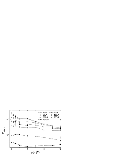
Figure 3 shows the dependence of normalized octave noise power on a magnetic field applied within the film plane parallel to the GB for different values of the bias current . Figure 3 shows two experimental facts. First, the noise power decreases with increasing bias current for all applied fields for A. Second, the noise power decreases with increasing magnetic field for bias current values below 500 A. Whereas for A the noise decreases by more than one order of magnitude by increasing the magnetic field up to 12 T, for A the noise is only weakly dependent on the applied magnetic field.
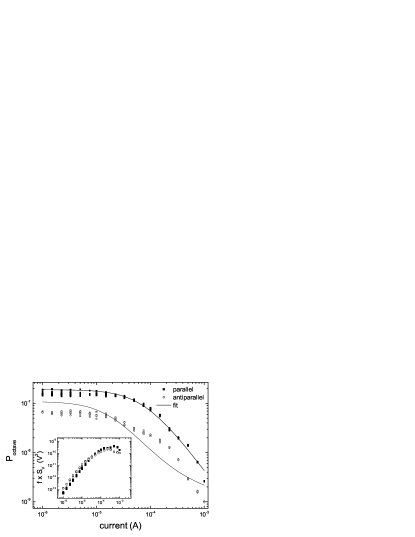
Figure 4 shows the detailed dependence of the normalized noise power on the bias current for both the parallel and antiparallel magnetization direction in the GBJ electrodes at K. It is evident that both for the parallel and antiparallel magnetization orientation there is only a very weak bias current dependence of the normalized noise power for small bias currents followed by a rapid decrease of at large bias current values. As illustrated in the inset of Fig. 4 the noise power shows a nonlinear dependence on the bias current.
III.2 Model considerations
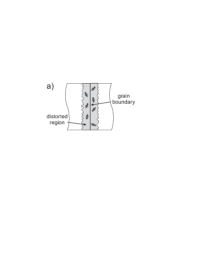
In the following we will argue that both the dc electrical transport and the low frequency noise properties can be consistently understood in a junction model assuming a strongly distorted region at the GB containing a large number of localized states/traps with fluctuating magnetic moments. A sketch of this junction model is shown in Figure 5a.
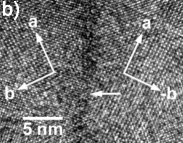
It is well known from the study of GBs in other perovskite materials (e.g. cuprate superconductors Gross94 ; Gross97 ) that strain, structural disorder and oxygen deficiency are important factors having a strong impact on the electrical transport properties. Figure 5b shows a high resolution transmission electron microscopy (HR-TEM) micograph of a symmetrical 36.8∘ [001] tilt GB in a film deposited on a SrTiO3 bicrystal substrate Gross00 . It is obvious that the grain boundary region is clean without any secondary phases and that the lattice distortions are confined to within a few lattice spacings. This is very similar to GBs in the cuprate superconductors, where the boundaries also were found to be clean without any secondary phases and with the lattice distortions to be confined within 1-2 lattice spacings Chisholm91a ; Kabius94a ; Seo95a . However, the grain boundaries in doped manganite epitaxial films are almost as straight as the GB in the underlying SrTiO3 bicrystal substrate. This is in clear contrast to GBs in the cuprate suberconductors that are strongly facetted Kabius94a ; Seo95a . It is very likely that this difference is related to the different growth modes of the cuprate and manganite thin films. Whereas the cuprates show a pronounced island growth with the islands growing across the substrate grain boundary resulting in strong facetting, the manganites show a molecular layer-by-layer growth mode Gross00 . In this growth mode it is expected that the grain boundary in the film follows exactly that of the substrate. We also have preliminary results that the microstructure of GBs in the manganites significantly depends on the deposition technique (e.g. laser-MBE, sputtering), the lattice mismatch between the film and the substrate and post-deposition annealing processes. However, more HR-TEM work is required for a detailed clarification of this issue.
For the cuprate GBs either a description in terms of a space-wise metal insulator transition at the grain boundary or in terms of band bending effects Mannhart96a ; Mannhart98a lead to a description of the GB as composed of an insulating layer at the barrier region which due to strain and structural disorder most likely contains a high density of localized defect states. Because of the structural affinity of the cuprate superconductors and the doped manganites it is very likely that also for these ferromagnetic junctions the transport properties are determined by an insulating tunnel barrier containing a large density of localized states Gross99a . Furthermore, there is already strong evidence for the presence of a significant density of localized states in the barrier from the fact that the current-voltage characteristics of the manganite GBJs can be very well described within the GM model (c.f. fig 1). Further evidence comes from the strong temperature and voltage dependence of the low field tunneling magnetoresistance Hoefener00 . Based on this experimental evidence we recently have proposed that the magnetotransport in manganite GBJs is determined by multi-step inelastic tunneling via magnetic impurity states within a disordered insulating GB barrier Klein99a ; Gross99a ; Hoefener00 .
Based on the model assumption of a large number of localized states within an insulating GB barrier there are two possible mechanisms which may be responsible for the observed low frequency voltage fluctuations. Firstly, the localized defect states are capable of trapping and releasing charge carriers. This charge carrier trapping and release processes lead to local variations of the barrier height and, thus, to fluctuations of the tunneling conductance. Furthermore, the magnetic field dependence of the noise (c.f. below) suggests that the charge traps are associated with a magnetic moment with a fluctuating orientation. Then, both the trapping and release of the charge carriers and, hence, the charge transport between the highly spin polarized electrodes depend on the local magnetic moment of the charge traps. Since the trapping and releases process depends on the relative orientation of the magnetic moment of the trap and the electrode magnetization, fluctuations of the direction of the magnetic moments of the charge traps strongly influence the local barrier transparency. A second mechanism giving rise to low frequency noise is related to coupling between the localized magnetic moments of the localized states and the spin of the tunneling electrons. Within the simplest approximation this coupling gives rise to an additional potential energy , where is the coupling constant and the angle between the localized moment and the electron spin. This additional energy, which is fluctuating with fluctuating orientation of the localized magnetic moments can be viewed as a fluctuation of the local barrier height.
Within the model of local barrier height fluctuations the dependence of the normalized voltage noise power on the bias current can be described within a small signal analysis based on the GM model. Doing so, we assume that the voltage fluctuations are caused by fluctuations of both the elastic and inelastic current contributions due to temporal variations of the local barrier height. Considering fluctuations of the elastic and inelastic and term, Eq. (3) gives for the small signal voltage fluctuation
where roughly corresponds to the total tunneling conductance. For independent fluctuations , and , the normalized voltage noise
| (5) |
is determined by the normalized fluctuations , and of the GM coefficients.
Analyzing Eqs (III.2) and (5) we can conclude the following: At low bias current (junction voltage) the elastic tunneling current is dominating and we can neglect the and terms and furthermore can use the approximation . Hence, for low bias current we expect , that is, a normalized noise power independent of the bias current (junction voltage). With increasing bias current (junction voltage) the inelastic tunneling contribution no longer can be neglected. This results in an increase of with increasing voltage and, hence, in an overall decrease of the of , even if the noise contributions of the inelastic channels increase with increasing voltage. As shown in Fig. 4 this behavior expected from our model consideration is in good qualitativ agreement with the measured data.
We even can go further and fit the data by Eq. (5). The solid lines in Fig. 4 are fits of Eq. (5) to the experimental data taking into account only fluctuations of the elastic and the first inelastic term. That is, and have been used as fit parameters, the term has been neglected to keep the number of fitting parameters minimum. We note that the GM coefficients and entering are obtained by fitting the current-voltage characteristics by the GM model prediction and therefore are fixed parameters in the fit of the noise data. Figure 4 shows that the small signal noise analysis based on the GM model is in good agreement with the experimental data for parallel magnetization alignment in the junction electrodes. The values for the normalized fluctuations in the elastic channel obtained from the numerical fits can be compared to the noise data of GBJs in cuprate superconductors, since , where are the normalized junction resistance fluctuations Marx97 . The normalized fluctuations nicely follow the scaling discussed in Ref. Marx97 for the cuprate superconductors. This scaling behavior has been discussed in terms of a constant density of trapping centers in the cuprate GBJs. Therefore the noise data of the manganite GBJs give further evidence of the close similarity to cuprate GBJs and suggest a similiar density of the noise centers in both junction types. Furthermore, and are found to depend only weakly on temperature in the investigated temperatur range below 80 K..
For the antiparallel magnetization orientation in the junction electrodes the modeling of the noise data by a small signal noise analysis based on the GM model is less convincing. However, Fig. 4 shows that a similar overall dependence of the normalized noise power on the bias current is observed for the antiparallel magnetization orientation. This is expected if we suppose that we can use the simple Jullière model Julliere75a to describe the ferromagnetic tunnel junction. Within this model the tunneling current is given by the tunneling matrix element and the density of states of the two spin directions at the Fermi level in the junction electrodes. Going from the parallel to the antiparallel configuration the tunneling matrix element stays the same. However, for a material with finite spin polarization the density of states for the spin-up and spin-down electrons is changed. Since in the elastic tunneling process the spin direction is conserved, a reduction of and is expected going from the parallel to the antiparallel magnetization orientation. It has been shown recently Hoefener00 that in the inelastic tunneling processes the spin direction does not seem to be conserved in manganite GBJs. Therefore, no reduction of and as well as is expected going from the parallel to the antiparallel magnetization orientation. Then, according to Eq. (5) we expect a slightly reduced value of and a similar functional dependence on the bias current (junction voltage). This is in qualitative agreement with the experimental data. We note, however, that the Jullière model certainly is too simple to describe the junction behavior in full detail. In particular, the assumption of a voltage independent density of states for the two spin directions may be an insufficient approximation. Recently, it has been shown that band structure effects give rise to voltage-dependent currents that conserve spin Cabrera02 . Summarizing our discussion we can conclude that our simple model based on a insulating tunneling barrier containing a high density of localized defect states already describes (at least for the parallel magnetization orientation) the measured noise data in a sufficient way. In order to get an even better agreement more sophisticated models have to be taken into consideration.
We now discuss the dependence of or, equivalently, on temperature. As shown by Figure 2, we observe an increase of with decreasing temperature. This is expected within our model due to the increase of the spin polarization in the junction electrodes with decreasing temperature Hoefener00 . In this case the fluctuating orientation of the localized magnetic moments within the GB barrier result in increasing fluctuations of the local barrier height. Whereas for a random orientation of the electron spin (zero spin polarization) a change of the direction of the local magnetic moments does not change anything and hence does not influence the tunneling probability, for a full orientation of the electron spins (100% spin polarization) each orientation of the localized magnetic moment corresponds to a different potential energy and hence a different local barrier height. That is with increasing spin polarization the fluctuations of the orientation of the localized moments results in increasing fluctuations of the local barrier height. We note that judging from the evaluation of the IVCs within the GM model the average barrier transparency is almost independent of temperature.
We next discuss the dependence of on the applied magnetic field. Applying a magnetic field was found to continuously decrease the junction noise up to 12 T for bias currents A as shown in Fig. 3. This can be explained within the proposed model in a straightforward way. The applied magnetic field tends to align the localized magnetic moments of the charge traps in the barrier region and thus reduces the fluctuations of the potential energy and, hence, the fluctuations of the local barrier height. We note, however, that in order to explain the magnetic field dependence of the noise power up to the largest applied field of 12 T (see Fig. 3) the fluctuating magnetic moments associated with the localized states cannot be considered as free moments but rather as (weakly) interacting moments forming a spin glass like state. It is well known that the physics of the doped manganites is determined by a competition of ferromagnetic double exchange and antiferromagnetic superexchange between neighboring Mn ions, which sensitively depends on doping as well as structural disorder and bond angles. Of course, for bulk the ferromagnetic double exchange is dominating. However, for the structurally distorted GB region there is certainly a strongly suppressed double exchange resulting in locally ferromagnetic and antiferromagnetic exchange Ziese98 . Because of this distorted nature of the GB it is plausible to assume that there is an arrangement of interacting magnetic moments strongly resembling a spin glass in the GB barrier.
We finally note that a spin polarized bias current of about 100 A corresponding to a current density of about A/cm2 flowing across the GB may result in a nonvanishing orientation of the localized magnetic moments. That is, in this scenario the spin polarized current is expected to have the same effect as an applied magnetic field, namely to reduce the low frequency noise. A reduction of the noise with increasing bias current has indeed been observed (see Fig. 4) but attributed above within the GM model to an increase of the inelastic tunneling current with increasing bias current (junction voltage). Since the functional form of the bias current dependence of the noise fits well to the GM model based explanation, we conclude that the orientation effect of the spin polarized current, although present, is small.

At low temperature ( K) we observed additional Lorentzian contributions to the low frequency noise as illustrated in Fig. 6. In contrast to the experiments in Refs. Mathieu01 ; Ingvarsson99 ; Ingvarsson00 these Lorentzians displayed various characteristic properties that are in obvious contradiction to the assumption of domain wall motion. First, we observe an evolution of the Lorentzians in time both at zero magnetic field (Fig. 6a) and at an applied magnetic field of T (Fig. 6b). Second, as shown in Fig. 6c) some Lorentzian components were found to be completely unaffected by applying a magnetic field as large as several hundred mT. Because of this ambiguous dependence on both time and magnetic field we suppose that the Lorentzians are due to an ensemble of interacting localized magnetic moments. The interaction between the moments leads to simultaneous switching of their direction between a discrete number of orientations. Random switching of the magnetization of such an ensemble between two distinct directions thus defines a two level system giving rise to random telegraph noise with a Lorentzian power spectrum. Furthermore, the independence of the Lorentzian contribution on the magnetic field shown in Fig. 6 also provides clear evidence against domain fluctuations in the junction electrodes as the origin of GBJ noise.

To further clarify the magnetic properties of the barrier region we have investigated the magnetic field dependence of the junction resistance down to 2 K and up to 16 T. Recently, in Refs. Klein99a ; Gross99a the distorted barrier has been modeled as a paramagnetic (PM) region even below the Curie temperature of the doped manganite, since the ferromagnetic double exchange is suppressed in the distorted GB layer. Since according to theoretical predictions Furukawa97 the paramagnetic insulator to ferromagnetic metal transition in the junction electrodes is expected to result in a large shift of the chemical potential, it has been argued that considerable band bending effects occur at the GB interface below . These band bending effects lead to a depletion of the paramagnetic GB layer. The width of this depletion layer is a function of the magnetization difference of the FM electrodes and the PM barrier with Klein99a ; Gross99a ; Furukawa97 . At low temperature and fields above the coercive field the magnetization of the ferromagnetic electrodes can be assumed constant and we have . The magnetization of the PM layer is determined by the Brillouin function, which is a function of . Then, we expect and, hence, . Then, the junction resistance is expected to follow . This is clearly not observed experimentally as shown in Fig. 7, where the two curves recorded at different temperatures do not coincide when plotted versus . Furthermore, for the Brillouin function can be approximated by . In this case is expected. Such behavior has indeed been reported Klein99a an also is shown in Fig. 7). However, for a paramagnetic GB layer at very low temperature and very high fields the behavior should be no longer valid, since the Brillouin function no longer can be approximated by . In contrast, the magnetization of the paramagnetic GB barrier is expected to saturate resulting in a saturation of the junction resistance. As shown by Fig. 7 this is clearly not observed in our experiments. Summarizing we can conclude that the absence of a scaling of the measured curves and of any saturation of the junction resistance at very high magnetic fields even at 2.3 K provides further evidence that the barrier region rather resembles a spin glass than a paramagnetic material in agreement with the the above conclusions drawn from the analysis of the noise data.
We also would briefly like to compare our noise data to that already available in literature. Recently, Mathieu et al. Mathieu01 investigated the noise of GB junctions in thin films. In these experiments the low frequency noise was found to show the same dependence on an applied magnetic field as the dc resistance. Therefore, the authors suggested that the measured low field noise is of magnetic origin related to domain fluctuations and domain wall motion in a multi-domain state neighboring the GB region. They further argued that the origin of the observed additional Lorentzian components in the low frequency noise are caused by thermally activated domain wall motion in this domain configuration.
Our noise data do not support this picture of a fluctuating magnetic state in the junction electrodes adjacent to the GB. The accurate description of both the IVCs and the noise data within the GM model strongly supports a tunneling-like mechanism for the charge transport and gives strong evidence that the low frequency noise in the manganite GB junctions is caused by the trapping and release of charge carriers in localized defect states within the GB barrier. Further support for the tunnel junction model stems from the dependencies Philipp00 . Here, for our GBJs an ideal two-level resistance switching with sharp transition from the low to the high resistance state is observed with the magnetic field applied parallel to the GB barrier resembling the rectangular shaped characteristics observed in TMR devices based on transition metals Jansen00 . Such dependencies would not be expected in the presence of a multi-domain state in the junction electrodes. Furthermore, the normalized octave noise of Fig. 3 shows a strong magnetic field dependence up to applied fields of 12 T especially at low bias currents. Again, this in contradiction to a multi-domain state, for which domain fluctuations are expected to be strongly suppressed at fields above about 1 T where the domains are fully aligned.
IV Summary
In summary, we performed a detailed analysis of the low frequency -noise in individual bicrystal grain boundary junctions formed in epitaxial films as a function of temperature, bias current, and applied magnetic field. Our noise data show that the low frequency noise in these junctions showing nearly ideal two-level resistance switching is due to localized sites with fluctuating magnetic moments in a strongly distorted barrier region. This is in full agreement with the description of the electrical transport properties of the GBJs by elastic and inelastic tunneling via localized defects states within an insulating grain boundary barrier. Low frequency noise due to domain fluctuations in the junction electrodes is found to play no significant role in the investigated samples. Additional Lorentzian contributions to the noise showing up at low temperature most likely are caused by clusters of interacting magnetic moments. The analysis of the electrical transport properties and the noise up to high magnetic fields suggests that the grain boundary barrier is rather a spin glass than a paramagnetic layer.
V Acknowledgment
The authors want to thank C. Höfener and J. Klein for valuable discussions. This work has been supported by the BMBF.
References
- (1) M. B. Salamon and M. Jaime, Rev. Mod. Phys. 73, 583 (2001).
- (2) F. Guinea, Phys. Solid State 35, 728 (1993).
- (3) H. Y. Hwang, S.-W. Cheong, N. P. Ong, and B. Barlogg, Phys. Rev. Lett. 77, 2041 (1996).
- (4) A. Gupta, G. Q. Gong, G. Xiao, P. R. Duncombe, P. Lecoeur, P. Trouilloud, Y. Y. Wang, V. P. Dravid, and J. Z. Sun, Phys. Rev. B 54, R15629 (1996).
- (5) N. D. Mathur, G. Burnell, S. P. Isaac, T. J. Jackson, B.-S. Teo, J. L. MacManus-Driscoll, L. F. Cohen, J. E. Evetts, and M. G. Blamire, Nature 387, 266 (1997).
- (6) K. Steenbeck, T. Eick, K. Kirsch, K. O’Donnell, and E. Steinbeiß, Appl. Phys. Lett. 71, 968 (1997).
- (7) J. Klein, C. Höfener, S. Uhlenbruck, L. Alff, B. Büchner, and R. Gross, Europhys. Lett. 47, 371 (1999).
- (8) R. Gross, L. Alff, B. Büchner, B. H. Freitag, C. Höfener, J. Klein, Y. Lu, W. Mader, J. B. Philipp, M. S. R. Rao, P. Reutler, S. Ritter, et al., J. Magn. Magn. Mater. 211, 150 (2000).
- (9) C. Höfener, J. B. Philipp, J. Klein, L. Alff, A. Marx, B. Büchener, and R. Gross, Europhys. Lett. 50, 681 (2000).
- (10) M. Ziese, Phys. Rev. B 60, R738 (1999).
- (11) J. B. Philipp, C. Höfener, S. Thienhaus, J. Klein, L. Alff, and R. Gross, Phys. Rev. B 62, 9248 (2000).
- (12) R. Gross, J. Klein, B. Wiedenhorst, C. Höfener, U. Schoop, J. B. Philipp, M. Schonecke, F. Herbstritt, L. Alff, Y. Lu, A. Marx, S. Schymon, et al., in Superconducting and Related Oxides: Physics and Nanoengineering IV, edited by D. Pavuna and I. Bosovic (2000), vol. 4058 of SPIE Conf. Proc., pp. 278–294.
- (13) B. Wiedenhorst, L. Alff, C. Recher, J. Klein, R. Gross, T. Walther, , and W. Mader, J. Magn. and Magn. Mat. 211, 16 (2000).
- (14) J. E. Evetts, M. G. Blamire, N. D. Mathur, S. P. Isaac, B.-S. Teo, L. F. Cohem, and J. L. MacManus-Driscoll, Trans. R. Soc. Lond. A 356, 1593 (1998).
- (15) J. M. D. Coey, A. E. Berkowitz, L. Balcells, F. F. Putris, and A. Barry, Phys. Rev. Lett. 80, 3815 (1998).
- (16) F. Guinea, Phys. Rev. B 58, 9212 (1998).
- (17) J. Zhang and R. M. White, J. Appl. Phys. 83, 6512 (1998).
- (18) A. Marx, U. Fath, W. Ludwig, R. Gross, and T. Amrein, Phys. Rev. B 51, 6735 (1995).
- (19) A. Marx, L. Alff, and R. Gross, Appl. Supercond. 6, 621 (1999).
- (20) T. Kemen, A. Marx, L. Alff, D. Kölle, and R. Gross, IEEE Trans. Appl. Supercond. 9, 3982 (1999).
- (21) G. B. Alers, A. P. Ramirez, and S. Jin, Appl. Phys. Lett. 68, 3644 (1996).
- (22) A. Lisauskas, S. I. Khartsev, and A. M. Grishin, J. Low Temp. Phys. 117, 1647 (1999).
- (23) H. T. Hardner, M. B. Weissman, M. Jaime, R. E. Treece, P. C. Dorsey, J. S. Horwitz, and D. B. Chrisey, J. Appl. Phys. 81, 272 (1997).
- (24) M. Rajeswari, A. Goyal, A. K. Raychaudhuri, M. C. Robson, G. C. Xiong, C. Kwon, R. Ramesh, R. L. Greene, T. Venkatesan, and S. Lakeou, Appl. Phys. Lett. 69, 851 (1996).
- (25) M. Rajeswari, R. Shreekala, A. Goyal, S. E. Lofland, S. M. Bhagat, K. Ghosh, R. P. Sharma, R. L. Greene, R. Ramesh, T. Venkatesan, and T. Boettcher, Appl. Phys. Lett. 73, 2672 (1998).
- (26) V. Podzorov, M. Uehara, M. E. Gershenson, T. Y. Koo, and S.-W. Cheong, Phys. Rev. B 61, 3784 (2000).
- (27) A. Anane, B. Raquet, S. von Molnár, L. Pinsard-Godart, and A. Revcolevschi, J. Appl. Phys. 87, 5025 (2000).
- (28) P. Reutler, A. Bensaid, F. Herbstritt, C. Höfener, A. Marx, and R. Gross, Phys. Rev. B 62, 11619 (2000).
- (29) A. Palanisami, R. D. Merithew, M. B. Weissman, and J. N. Eckstein, Phys. Rev. B 64, 132406 (2001).
- (30) B. Raquet, A. Anane, S. Wirth, P. Xiong, and S. von Molnár, Phys. Rev. Lett. 84, 4485 (2000).
- (31) R. D. Merithew, M. B. Weissman, F. M. Hess, P. Spradling, E. R. Nowak, J. O´Donnell, J. N. Eckstein, Y. Tokura, and Y. Tomioka, Phys. Rev. Lett. 84, 3442 (2000).
- (32) F. M. Hess, R. D. Merithew, M. B. Weissman, Y. Tokura, and Y. Tomioka, Phys. Rev. B 63, 180408 (2001).
- (33) R. Mathieu, P. Svedlindh, R. Gunnarson, and Z. G. Ivanov, Phys. Rev. B 63, 132407 (2001).
- (34) L. I. Glazman and K. A. Matveev, Sov. Phys. JETP 67, 1276 (1988).
- (35) R. Gross, in Interfaces in Superconducting Systems, edited by S. L. Shinde and D. Rudman (Springer, New York, 1994), pp. 176–209.
- (36) R. Gross, L. Alff, A. Beck, O. M. Froehlich, D. Koelle, and A. Marx, IEEE Trans. Appl. Supercond. 7, 2929 (1997).
- (37) M. F. Chisholm and S. J. Pennycook, Nature 351, 47 (1991).
- (38) B. Kabius, J. W. Seo, T. Amrein, U. Dahne, A. Scholen, M. Siegel, K. Urban, and L. Schultz, Physica C 231, 123 (1994).
- (39) J. W. Seo, B. Kabius, U. Dahne, A. Scholen, and K. Urban, Physica C 1995, 25 (245).
- (40) J. Mannhart, Supercond. Sci. Techn. 9, 49 (1996).
- (41) J. Mannhart and H. Hilgenkamp, Mater. Sci. and Eng. B 56, 77 (1998).
- (42) A. Marx and R. Gross, Appl. Phys. Lett. 70, 120 (1997).
- (43) M. Jullière, Phys. Lett. A 54, 225 (1975).
- (44) G. G. Cabrera and N. Garcia, Appl. Phys. Lett. 80, 1782 (2002).
- (45) M. Ziese, C. Srinitiwarawong, and C. Shearwood, J. Phys.: Condens. Matter 10, L569 (1998).
- (46) S. Ingvarsson, G. Xiao, R. A. Wanner, P. Trouilloud, Y. Lu, W. J. Gallagher, A. Marley, K. P. Roche, and S. S. Parkin, Appl. Phys. Lett. 85, 5270 (1999).
- (47) S. Ingvarsson, G. Xiao, S. S. Parkin, W. J. Gallagher, G. Grinstein, and R. H. Koch, Phys. Rev. Lett. 85, 3289 (2000).
- (48) N. Furukawa, J. Phys. Soc. Jpn. 66, 2523 (1997).
- (49) R. Jansen and J. S. Moodera, Phys. Rev. B 61(13), 9047 (2000).