Temperature dependent deviations from ideal quantization of plateau conductances in GaAs quantum point contacts
Abstract
We present detailed experimental studies of the temperature dependence of the plateau conductance of GaAs quantum point contacts in the temperature range from 0.3 K to 10 K. Due to a strong lateral confinement produced by a shallow-etching technique we are able to observe the following unexpected feature: a linear temperature dependence of the measured mid-plateau conductance. We discuss an interpretation in terms of a temperature dependent, intrinsic series resistance, due to non-ballistic effects in the 2D-1D transition region. These results have been reproduced in several samples from different GaAs/GaAlAs-heterostructures and observed in different experimental set-ups.
1 Introduction
More than a decade after the first observation of quantized conductance, the quantum point contact (QPC) remains a central research topic in mesoscopic physics. QPCs are often employed as basic components in mesoscopic experiments, and more recently they are playing a central role in studies of spin-related physics such as spin filtering [1], quantum entanglement [2], the Kondo effect [3], and single-photon generation [4]. These applications necessitate a detailed understanding of the QPC, and this is the motivation for our work.
In this paper we present experimental observations of a novel temperature effect in GaAs QPCs: a linear temperature dependence of the measured mid-plateau conductance. As in previous work [5] our new experiments rely on a shallow-etch technique in the fabrication of the QPC, which yields particularly strong lateral confinement. This enables studies of the temperature dependence of the quantized QPC conductance up to 10 K.
2 Sample fabrication
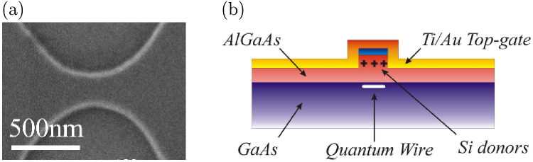
The QPCs were fabricated on 2-dimensional electron gases (2DEGs) defined in modulation doped GaAs/GaAlAs heterostructures. Typical 2DEG mobilities and densities were 70-100 m2/Vs and 21015 m-2, respectively. The narrow QPC constrictions were defined by shallow wet etching as described in Ref. [5]. The phenomena discussed here were observed in three different experimental set-ups and on several samples. We present data from one particular sample, shown in Fig. 1a. The electron density in the shallow etched QPC-constriction (approximately 200 nm wide and 200 nm long) is controlled by a 10 m wide Ti/Au topgate electrode, with an applied voltage denoted , covering that region. The samples have an energy spacing of the two first transverse subbands of 5-10 meV. The samples are situated on a 20 m wide and 100 m long mesa, with several ohmic contacts.
3 Measurements
The sample was mounted in a pumped 3He cryostat, enabling measurements in the temperature range from 0.3 to 10 K. The differential conductance, was measured in a 2-point voltage controlled setup, using a standard lock-in technique at 117 Hz. Here is the source-drain voltage bias and the corresponding current.
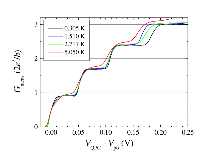
In Fig. 2 we show raw data plots of the gate-characteristics, i.e. the measured conductance, , versus gate voltage, , taken at different temperatures. The pinch-off voltage, , is defined as . For the raw data, the conductance plateaus do not coincide with the expected integer quantization. This is, in part, due to an inevitable series resistance.
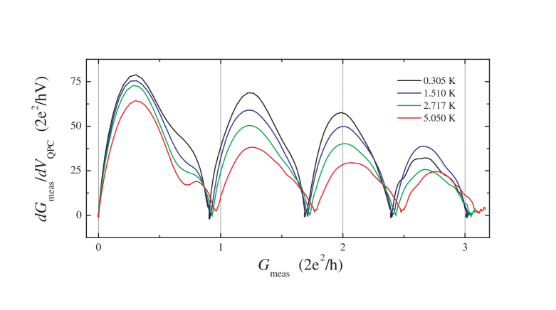
We want to study the plateau conductance, which we define by the conductance value at the point of minimal slope of the gate characteristics. To extract these values, we plot the transconductance, , versus conductance, , as shown in Fig. 3. We note that on this plot the sharp minima, identifying the plateau conductance on the four plateaus, exhibit a remarkable increase with temperature. This temperature dependence is the central issue of our work.
4 Data analysis
In the data analysis we use the plateau conductance values to extract information about the series resistance. However, the observed temperature dependence of the plateau conductances complicates this analysis. In general, the measured resistance, , can be written as a combination of the resistance of the QPC, , and the series resistance, :
| (1) |
A crucial point is to relate the plateau conductance of the ’th plateau to the conductance quantum, . As seen in Fig. 2 and Fig. 3, the plateaus are well defined, which can justify the most simple assumption,
| (2) |
In this case, which is analyzed in Sec. 4.1, the observed temperature dependence of the plateau conductances is attributed solely to the series resistance.
The temperature dependence could also be interpreted in terms of a temperature dependent coefficient, , in front of the conductance quantum
| (3) |
This assumption is analyzed in Sec. 4.2.
4.1 Temperature and gate voltage dependent and constant coefficient
We begin with the most simple assumption, namely Eq. (2) stating that the QPC conductance is given by times the conductance quantum. This assumption is justified by the high quality of the observed conductance plateaus. In terms of Eq. (3) this corresponds to fixing the coefficient , so the only free parameter in Eq. (1) is the series resistance .
For each mid-plateau conductance extracted from Fig. 3, it is now possible to calculate a value of . For a given plateau at a given temperature we assign to the value of displaced by as in Fig. 2. Thus we obtain a temperature and gate voltage dependent series resistance shown in Fig. 4. The series resistance is seen to depend strongly on temperature and gate voltage.
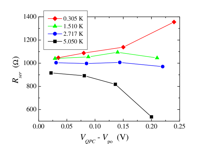
We keep in mind that the measured conductance include approximately 10020 m of 2DEG, in addition to the QPC constriction. So the question naturally arises if the series resistance in Fig. 4 could be a bulk 2DEG resistance. For temperatures smaller than the maximum temperature of 10 K used here, the resistance of the unpatterned 2DEG is basically constant. The strong temperature dependence of seen in Fig. 4 (a change of more than a factor of at the last plateau), makes it very implausible that the series resistance is solely due to the resistance of the 2DEG.
The same conclusion can be drawn from the gate voltage dependence. The gate controlling the electron density in the QPC also covers approximately 1020 m of the 2DEG. Therefore the series resistance of the 2DEG will change with gate voltage by a fraction of the ungated square resistance, 50 . But the resistance of the 2DEG will be monotonically decreasing with increasing gate voltage. This is contradiction with the data points in Fig. 4 for the lowest temperatures.
We conclude that series resistance extracted from the measured conductance plateaus, shows a remarkable dependence on temperature and gate voltage. It cannot be attributed to the resistance of the bulk 2DEG, in which the quantum point contact is situated. We will discuss other interpretations of the extracted series resistance in Sec. 5.
4.2 Temperature dependent resistance and coefficient

We now allow in Eq. (3) to depend on temperature, and assume to be independent of gate voltage but varying with temperature. We plot the resistance value of the ’th conductance plateau , as function of in Fig. 5. With Eq. (1) and (3) this allows us to extract and , shown in Figs. 6a and 6b, respectively. The series resistance basically remains constant as function of temperature. However, increases linearly as temperature is raised from to K.
A temperature dependent plateau conductance of quantum wires has earlier been reported, e.g., in Ref. [6], and interpreted in the context of Luttinger liquid physics combined with disorder in the wires. Here a similar interpretation is not possible. The Luttinger liquid theory applies for extended 1D systems, whereas our system only has a length of 200 nm, which is a few Fermi wavelengths and similar to the width. Additionally, the effect of such electron-electron correlations should be a suppression of the conductance below the quantized value. Here we observe a conductance plateau that at one temperature is clearly below the quantized value and at another clearly above. This effect is larger than the error bar on the calibration of the resistance measurement setup. We note that a temperature dependent plateau conductance has also been reported for a different quantum wire system [7]. Here the conductance was only reduced below the quantized value (), a result that could be interpreted in terms of scattering across a 2D-1D interface [8, 9].
We conclude that the temperature dependence of the height of the conductance plateaus, can be described by a temperature dependent overall rescaling of the conductance, and a temperature and gate voltage independent series resistance.


5 Discussion
We have presented measurements of quantized conductance in a shallow-etched GaAs QPC in the temperature range from 0.3 K to 10 K. The four well-defined conductance steps show on close inspection a temperature dependent deviation from the expected quantization value. The deviation cannot be accounted for by describing our system as a simple series connection of a 2DEG and an ideal quantum point contact. We have observed this effect in several different devices, with both 2-point and 4-point measurement schemes.
We can assign correct values to the measured conductance plateaus by allowing an overall conductance rescaling factor to vary (a few percent) with temperature. The small length of our device and the fact that we can measure greater than unity depending on temperature, rules out Luttinger liquid corrections as the cause of our findings. We can alternative describe the deviations from the quantized conductance values by an effective series resistance , which depends strongly on gate voltage and temperature. We underline that the parameter dependence of is incompatible with that of a pure bulk 2DEG resistance.
The above discussion has rejected intrinsic 1D or 2D effects as the origin of the observed deviations from conductance quantization. This suggests that non-ballistic effects in the 1D-2D contact region are the cause instead. The high quality of the conductance pleateaus makes it implausible that reflection takes place in the QPC itself. Reflections in the contact region can of course only decrease the plateau conductance below its quantized value. The non-trivial temperature and gate voltage dependence of the resulting effective series resistance (Fig. 4), which results from this interpretation, points to an intricate effective potential landscape in the contact region, which deserves further experimental and theoretical investigation. We remark that the nature of the 1D-2D contact region is very different from that of the quantum wires in Refs. [7, 9], so in our case is not possible to take over straightforwardly the interpretations presented in Refs. [8, 9].
Acknowledgements
We thank C.B. Sørensen for growing the semiconductor structures, and P.E. Lindelof for hosting the experiments. This work was partly supported by the Danish Technical Research Council (grant no. 9701490) and by the Danish Natural Science Research Council (grants no. 9502937, 9600548 and 9601677). The III-V materials used in this investigation were made at the III-V NANOLAB, operated jointly by the Microelectronics Centre, Technical University of Denmark, and the Niels Bohr Institute, University of Copenhagen.
References
References
- [1] K.J. Thomas et al., Phys. Rev. Lett. 77, 135 (1996)
- [2] R.C. Liu et al., Nature 391, 263 (1998)
- [3] S.M. Cronenwett et al., Phys. Rev. Lett. 88, 226805 (2002)
- [4] EU-project SAW-PHOTON, http://ntserv.fys.ku.dk/sawphoton/
- [5] A. Kristensen et al., Phys. Rev. B 62, 10950 (2000)
- [6] S. Tarucha et al., Solid State Comm. 94, 413 (1995)
- [7] A. Yacoby et al., Phys. Rev. Lett. 77, 4612 (2000)
- [8] A. Yu. Alekseev and V. V. Cheianov, Phys. Rev. B 57, R6834 (1998)
- [9] R. de Picciotto et al., Phys. Rev. Lett. 85, 1730 (2000)