Phase diagram as a function of temperature and magnetic field for magnetic semiconductors.
Abstract
Using an extension of the Nagaev model of phase separation (E. L. Nagaev, and A. I. Podel’shchikov, Sov. Phys. JETP, 71 (1990) 1108), we calculate the phase diagram for degenerate antiferromagnetic semiconductors in the plane for different current carrier densities. Both, wide-band semiconductors and “double-exchange” materials, are investigated.
pacs:
75.90.+wI Introduction
Degenerate antiferromagnetic semiconductors are obtained by strongly doping antiferromagnetic semiconductors (e.g., europium chalcogenides or lanthanium manganites). Over a concentration range of doping impurities, the ground state of these compounds will be a mixture of antiferromagnetic (AF) and ferromagnetic (FM) phases Nagaev (1983, 1972); Kashin and Nagaev (1974). Starting from a pure compound and doping, we find that the ground state at is AF and non-conducting up to some conduction electron concentration driven by impurities, , from which the homogeneous state turns out to be unstable against phase separation. The ground state becomes then inhomogeneous with a simply connected AF phase and a multiply connected FM phase. The exact geometry of the multiply connected phase is of fractal nature. On increasing doping, a geometric transition takes place in which the topology of the sample changes due to percolation of the FM phase. Now, the ground state corresponds to a multiply connected AF phase and a simply connected FM one. The doping concentration at which this transition occurs is denoted by . At this point an important change in the conductivity is expected, the material becomes a conductor. On a further increase of doping, a certain concentration, , exits at which this phase-separated state starts to be unstable and the sample becomes again homogeneous but now FM. The physical reason for having a phase-separated state in an antiferromagnetic semiconductor at is the dependence of the energy of the charge carriers that appear on doping on the magnetic order of the lattice. The charge carrier energy is lower if they move in a FM region. Therefore, by interaction with the spin system in the lattice, they are able to change its magnetic order, creating FM micro-regions and become trapped in them. In a degenerate magnetic semiconductor this is a cooperative phenomenon: a number of electrons are self-trapped in the same FM micro-region diminishing the energy per electron necessary to create it. When the carrier concentration is high enough, the phase-separated state turns out to be stable. For the free energy has different expressions for the AF and the FM parts. Because of this, a change in the temperature or the magnetic field produces a variation of the relative volume of the AF and FM parts. Therefore, a temperature- or magnetic field-induced percolation can occur, resulting in a complicated phase diagram.
In this article, we calculate the phase diagram in the plane for magnetic semiconductors within the doping range . The phase diagram is expected to be divided into three different stability regions, those corresponding to: insulating phase-separated state, conductive phase-separated state and homogeneous state. Our calculations are based in a variational principle for the free energy of the system developed by Nagaev and Podel’shchikov in the reference Nagaev and Podelsh’chikov (1990) that generalizes the approach of the references Nagaev (1983, 1972); Kashin and Nagaev (1974) to the case of finite temperature.
II Calculation of the free energy
In this section, we briefly review the variational method used. More detailed calculations can be found in references Nagaev (1983, 1972); Kashin and Nagaev (1974); Nagaev and Podelsh’chikov (1990). The microscopic description of the sample is provided by the Hamiltonian of the generalized Vonsovsky s-d model. The main parameters in this model are , the carriers band-width, the exchange energy between conduction electrons and magnetic ions (s-d exchange energy), and the exchange energy between magnetic ions (d-d exchange energy). is the exchange integral between first-nearest neighbors magnetic ions. The smallest parameter is the d-d exchange energy. We differentiate two possibilities depending on the relative value of and . In the case , we have a wide-band semiconductor (e.g. ). In the opposite case , we talk about a “double-exchange” material (e.g. lanthanium manganites). For the sake of definiteness the sign of is assumed to be positive.
The free energy is expresed as a function of two variational paramaters: the ratio of the volumes of the AF and FM phases, , and , the radius of the spheres which form the multiply-connected phase. All of the electrons are assumed to be found in the FM part of the phase-separated state González et al. (2002). Although this is not strictly true at , it is a good approximation because the number of electrons in the AF part is proportional to , where if or if , and in both cases we have . The trial free energy is given by the expression:
| (1) |
where is the standard bulk kinetic energy of the conduction electrons, is the surface electron energy, i.e. the correction to that appears due to the quantization of the electron motion in regions of finite dimensions Balian and Bloch (1970). In view of the degeneracy of the electron gas, the contribution of the thermal excitations to its free energy can be neglected. is the electrostatic energy due to the inhomogenous electronic density and is the magnetic free energy calculated in the mean field approximation. Due to the absence of conduction electrons on the AF part of the phase-separated state, this trial free energy is valid for both and .
The expressions for these quantities are:
| (2) |
| (3) |
where and if the FM part is multiply connected, or if it is simply connected. The Coulomb energy per unit cell is found by separation of the crystal into Wigner cells. This method provides a good approximation to the electrostatic energy for small volumes of the alien phase, but it supposes to admit that the crystal is isotropic and homogeneous regarding the spatial distribution of these spheres. So we cannot describe the fractal nature of the boundary that separes both phases.
The free energy of the magnetic system is calculated using the mean field approximation. It is assumed that in the FM part conduction electrons are completely polarized. Then:
| (4) |
where:
| (5) |
and the values verify the following equations:
| (6) |
where is the Brillouin function. Moreover, we have defined as the mean field created by the conduction electrons on the localized d-spin system. The preceding energies where obtained taking into account that in the case of small fields, , the localized d-spins system is in a non-collinear AF (NCAF) state, being the mean d-spin value in each of the sub-lattices. In the case of high fields, , the sample goes to a non-saturated FM (NSFM) state, being the mean value of the localized d-spin per site Nagaev (1983).
III Results.
The stationary state of the system is determined from the condition that the total free energy of the system, equation (1), be a minimum with respect to the variational parameters and . The parameter only appears in the surface and Coulomb energies. Minimizing the sum with respect to for fixed leads to the following expression:
| (7) |
where the following definitions are used:
| (8) |
After substitution of equation (7) in equation (1) minimization with respect to is carried out numerically.
For three different phases are expected: insulating phase-separated, conducting phase-separated and homogeneous states. We calculate the regions of absolute stability of each phase in the plane for different conduction electron concentrations in the sample. The boundary lines between phases are calculated numerically. Below we present these diagrams for different concentrations, all below , for both wide-band Nagaev and Podelsh’chikov (1990) and “double-exchange” materials.
Our results indicate that for both kinds of materials, all of the phase transitions between homogeneous and phase-separated states are first-order. Preliminary calculations including the possibility of spin waves confirm this result Nagaev (2000). The transition between insulator and conductive phase-separated states is found close to second-order. The jump in the parameter at the transition is about at , growing with the transition temperature. This small jump in the parameter does not permit elucidating whether in a real sample the transition is of first- or second-order. We have to stress that the boundary between the separate states is of a fractal nature, and our approximation, that considers it as homogeneous and isotropically distributed spheres, does not work near the transition point. In any case, due to the smallness of the jump in our approximation provides accurate values of and at the transition point.
III.1
Phase diagrams for wide-band semiconductors are shown in figures (3), (3) and (3) for conduction electron concentrations equal to , respectively. The areas 1, 2, 3 denote regions of absolute stability for the homogeneous state, the conductive phase-separated state and the insulating phase-separated state, respectively. The parameters that characterize these materials are chosen to be the same as in reference Nagaev and Podelsh’chikov (1990) (they correspond to rare-earth compounds like europium chalcogenides): , eV (implying K, and the field at which both sublattices collapse is kOe), eV, , cm-3, and the electron effective mass is equal to free electron mass, this implies eV. The value obtained for cm-3. The value for , at which the conducting phase-separated state becomes unstable at , is cm-3.

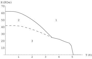
We see that at low carrier concentrations only a transition from the insulating phase-separated state to the homogeneous state is possible (see figure (3)). The physical explanation of the diagram (3) is the following. At fixed , the effect of the increase of magnetic field and temperature is to decrease the value of with respect to its value at . In the range of concentrations we are working, , the state of the sample at is an insulating phase-separated state (). Regarding to the behavior of at with , as . Following equations (4), the d-spins of the magnetic ions in the FM part of the phase-separated state experience a magnetic field which is the sum of the external field, , and an additional field created by conduction electrons, . If we set the external field equal to zero, is large enough to establish the FM order in the multiply-connected part, i.e. . But as we increase external field, the value of decreases very quickly and it is reached a point in which . On further increase of , the magnetic field cannot maintain the multiply-connected part in a FM (NSFM) state and a transition to an homogeneous AF (NCAF) state occurs. The transition line can be drawn in a simple approximate way. We start by looking for the value of , , which makes the energy minimal at . For we found . Because this value increases only slightly as we move along the transition line, this can be approximated by the expression .
At for , the carrier concentration is high enough to permit that increasing the external field we remain in the insulating phase-separated state until . Therefore for concentrations , three different phases appear. At low temperatures and low magnetic fields, we have a transition between both of the phase-separated states. This line correspond to the simultaneous percolation of the magnetic order and the conduction electron system. It is almost a second order transition. The values of at both sides of the transition line are and at not varying with , increasing as we move along the line towards higher temperatures, and being the growth smaller, the closer to . To calculate the values of (being the values of at both sides of the transition line), we impose three conditions: the free energy of both phase-separated states must have a minimum and the free energy of both states must be equal. This allows us to calculate varying along the line. Over the same range of temperatures but at higher fields, we find a transition between conductive phase-separated and an homogeneous state. This is a first order transition, similar to the melting of a solid. Again the same effect than in diagram (3) appears once we are in the conductive phase-separated state, the value of must be high enough to maintain the simply-connected in a FM state. If not, a first-order transition to an homogeneous state with a value of approximately constant along the line occurs.
In figure (3), is high enough to permit that increasing the magnetic field we remain in the conducting phase-separated state until , so this effect is absent. In this case the transition line is determined in the same way as in the usual melting transition Landau and Lifshits (1988). To calculate the value of , we impose the conditions that the first two derivatives of the free energy of the conductive phase-separated state be equal to zero. At higher temperatures we find the transition line between the insulating phase-separated and homogeneous states, that now corresponds to a NSFM order. It is important to notice that what we denote as phase 1 in the diagrams, corresponds only to homogeneous magnetic states, without distinguishing whether they are of the NCAF or NSFM type. This is the reason why a kink in the transition line appear at K. Really, it corresponds to a tri-critical point between insulating phase-separated, homogeneous NSFM states (at lower temperatures) and homogeneous NCAF (at higher temperatures). The transition line between these two is not drawn. The transition line from the kink to the -axis correspond to the magnetic transition of the AF part of the insulating phase-separated state to a PM state. With , this tri-critical point tends to the point . Due to the absence of electrons in the AF part of the phase-separated states the whole the sample has the same Néel temperature, as is confirmed by experiment. This part of the line is calculated in the same way that the transition line between conductive phase-separated state and homogeneous states.
The third diagram corresponds to . We find two transition lines. One between both of the phase-separated states, close to second order, as in the preceding discussion. We see that now the tricritical point between conductive phase-separated, insulating phase-separated and homogeneous states is absent. Therefore the percolation with temperature (this is, at ) is also possible. The other line corresponds to the transition between conductive phase-separated and homogeneous states (now, NSFM all along the line). The kink was moved to higher temperatures. We see that the region of absolute stability of the insulating phase-separated state has been reduced, tending to dissappear as goes to .
III.2
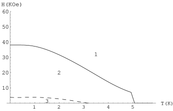
Phase diagrams for “double-exchange” semiconductors are essentially the same. We also present three of them, in figures (6), (6), and (6), corresponding to conduction electron concentrations equal to , respectively. The parameters that characterize “double-exchange” semiconductors are the following (typical for lanthanium manganites, for example) Nagaev (2001a): , eV (that implies K, and the field at which the two sublattices collapse at is MOe), , cm-3, the effective electron mass equal to the free electron mass, that implies eV and eV. With these parameters we obtain cm-3 and cm-3.


The behavior of the “double exchange” compounds is quantitatively different. The scenario discussed above for wide-band case remains valid, but a higher value of implies a very strong magnetic field acting on the FM part of the separate states and also a higher value of . It must be stressed that the values that we obtain for , are far from the true theoretical values. In particular, the values obtained depend on the physical parameters such as , while we are dealing with a geometric transition that cannot depend on these details. This is because we lost the fractal nature of the surface that separes phases to simplify calculations. The quantum nature of the d-spin system forces the true percolation concentration to be , the percolation concentration for the Bethe lattice (see, for example, Efros (1994)), independently of the physical processes involved. So, in both cases treated here, it is necessary to “map” in order to compare with the experimental values. Because we can neglect the terms with in the partition function of the FM part. This makes the FM part temperature-independent, remaining in the same state as at . We see in figures (6) and (6), that the tri-critical point corresponding to the kink at K, is now between conductive phase-separated, homogeneous NSFM (at lower temperatures) and homogeneous NCAF (at higher temperatures), and appears before in temperature than the tri-critical point between conductive phase-separated, insulating phase-separated and homogeneous state (now, NCAF). As we see in figure (6), percolation is possible varying the magnetic field in the same way as above, but percolation in temperature (i.e. at ) is not, contrary to what was seen above. However, this result can be modified beyond a mean field approximation. It must also be stressed that the value of sets the scale of the -axis and its high value makes the transition to the homogeneous states occur to unphysical values of the external field.
A comparison with the experimental results is specially relevant for the case of “double-exchange” compounds. It must be stressed that although all along this article we talk about the charge carriers as being conduction electrons, the model is general enough to deal also with hole-doped compounds. An example of the latter could be the canonical CMR lanthanium manganite La1-xCaxMnO3 with , which is extensively reviewed in the reference Nagaev (2001b). However the present calculation is more interesting for electron-doped compounds, such as Sm1-xCaxMnO3 with , because the region of record negative magnetoresistance fall within the range of doping studied in this work. This compound is studied in the reference Algarabel et al. (2002), where the observed CMR effects are explained as consequence of the metal-insulator transition described here. They also present the phase diagram in the plane for th compound Sm0.15Ca0.85MnO3, which agrees qualitatively and quantitatively with our figure (6).
Acknowledgements.
The authors are deeply indebted to Prof. E. L. Nagaev for his encouragement and help during its realization. Unfortunately, Prof. Nagaev died recently. This article is dedicated to his memory.References
- Nagaev (1983) E. L. Nagaev, Physics of magnetic semiconductors (Mir, Moscow, 1983).
- Nagaev (1972) E. L. Nagaev, Sov. Phys. JETP Lett. 16, 394 (1972).
- Kashin and Nagaev (1974) V. A. Kashin and E. L. Nagaev, Sov. Phys. JETP 39, 1036 (1974).
- Nagaev and Podelsh’chikov (1990) E. L. Nagaev and A. I. Podelsh’chikov, Sov. Phys. JETP 71, 1108 (1990).
- González et al. (2002) I. González, J. Castro, and D. Baldomir, Phys. Lett. A 298, 185 (2002).
- Balian and Bloch (1970) R. Balian and C. Bloch, Ann. Phys. 60, 401 (1970).
- Nagaev (2000) E. L. Nagaev, Phys. Rev. B 62, 5751 (2000).
- Landau and Lifshits (1988) L. D. Landau and I. M. Lifshits, Física Estadística (Statistical Physics) (Reverté, Barcelona, 1988).
- Nagaev (2001a) E. L. Nagaev, Phys. Rev. B 64, 14401 (2001a).
- Efros (1994) A. L. Efros, Geometría y física del desorden (Geometry and Physics of disorder) (URRS, Moscow, 1994).
- Nagaev (2001b) E. L. Nagaev, Phys. Rep. 346, 387 (2001b).
- Algarabel et al. (2002) P. A. Algarabel, J. M. D. Teresa, B. García-Landa, L. Morellon, M. R. Ibarra, C. Ritter, R. Mahendiran, A. Maignan, M. Hervieu, C. Martin, et al., Phys. Rev. B 65, 104437 (2002).