Spectroscopic determination of hole density in the ferromagnetic semiconductor Ga1-xMnxAs
Abstract
The measurement of the hole density in the ferromagnetic semiconductor Ga1-xMnxAs is notoriously difficult using standard transport techniques due to the dominance of the anomalous Hall effect. Here, we report the first spectroscopic measurement of the hole density in four Ga1-xMnxAs samples () at room temperature using Raman scattering intensity analysis of the coupled plasmon-LO-phonon mode and the unscreened LO phonon. The unscreened LO phonon frequency linearly decreases as the Mn concentration increases up to . The hole density determined from the Raman scattering shows a monotonic increase with increasing for , exhibiting a direct correlation to the observed . The optical technique reported here provides an unambiguous means of determining the hole density in this important new class of “spintronic” semiconductor materials.
Accepted for publication in Physical Review B (tentatively scheduled to appear in 15 July 2002 issue)
Current interest in the development of a semiconductor “spintronics” technology wolf01 provides a strong motivation for fundamental studies of diluted magnetic semiconductors (DMS) furdyna88 ; awssam99 ; ohno99 . These are semiconductors that incorporate magnetic ions such as Mn2+ within the crystal lattice. Paramagnetic (and antiferromagnetic) DMS have traditionally been realized by incorporating isovalent transition metal ions into II-VI semiconductors such as CdTe and ZnSe. furdyna88 ; awssam99 The relatively recent discovery of ferromagnetic III-V semiconductor-based DMS with Curie temperatures () as high as 110 K has now raised interesting fundamental issues regarding the origin of ferromagnetism in materials such as Ga1-xMnxAs. dietl00 ; ohno96 ; deboeck96 In these III-V DMS, Mn2+ acts as an acceptor, generating free holes in the valence band. matsukura98 The ferromagnetism in these materials arises from the exchange interaction between these holes and the Mn2+ ions, and it is generally believed that there is a direct correlation between and the hole density . dietl00 ; konig00 However, the unambiguous determination of the hole density in Ga1-xMnxAs by standard magneto-transport techniques (Hall measurement) is difficult because of the anomalous Hall effect. The extraction of the ordinary Hall effect from the measurement, applied at , requires magnetic fields larger than 20 T even at temperatures as low as 50 mK; even under these conditions, the measured Hall data are not completely free from the effect of the negative magnetoresistance, resulting in significant uncertainty in the deduced hole density. In addition, Hall measurements are not applicable to magnetically dilute samples that are insulating. ohno99 Finally, we note that the Curie-Weiss law behavior of the magnetic susceptibility determined by the Hall effect clearly indicates the dominance of the anomalous Hall effect over the ordinary Hall effect even at room temperature. ohno01 Here, we exploit an alternative method (Raman scattering) to determine the hole density in Ga1-xMnxAs epilayers for a wide range of temperatures by correlating the hole density to the coupled plasmon-LO-phonon mode (CPLOM). mooradian66 ; irmer97 Our results show that this spectroscopic technique provides a reliable method for determining the hole density in ferromagnetic semiconductors over a broad range of sample conductivity, ranging from insulating to highly metallic.
For -type GaAs, the coupling between the LO phonon and electron plasmon results in two Raman active coupled plasmon-LO-phonon modes (CPLOM), and . For high electron density, shows a rapid blue-shift with increasing electron concentration, providing an accurate calibration for the electron concentration, whereas remains almost stationary near the GaAs TO frequency. On the other hand, only one CPLOM is observed in -type GaAs due to a strong hole plasmon damping, moving from the LO to the TO frequency with increasing hole concentration. irmer97 In this paper, we report the spectroscopic determination of the carrier concentration of four Ga1-xMnxAs samples () at room temperature using Raman scattering from CPLOM. We find that the unscreened LO (ULO) phonon frequency of Ga1-xMnxAs decreases significantly as the Mn concentration increases up to . This makes the traditional lineshape analysis for a typical p-type GaAs, where the doping does not change the ULO frequency, unsuitable for determining the hole density in Ga1-xMnxAs. By analyzing the relative Raman intensities of the ULO phonon and the CPLOM, however, we were able to determine the carrier concentration up to . The monotonic increase of the hole density with increasing for correlates well with the change of .
Ga1-xMnxAs epilayers with thickness of were grown by molecular beam epitaxy at on a (001) semi-insulating GaAs substrate after the deposition of a buffer structure consisting of a standard GaAs epilayer grown at followed by a low-temperature grown GaAs epilayer. Electron microprobe analysis (EMPA) was used to determine Mn concentrations. Details about the growth conditions and parameters are described elsewhere. potashnik01 Raman scattering measurements were performed at room temperature in a quasi-backscattering geometry on the (001) growth surface of the samples. The line from a Coherent Ar+ laser was used as an excitation light source in order to obtain a very short penetration depth, thus avoiding any Raman scattering from the buffer layers. The scattered photons were dispersed by a SPEX - triple spectrometer and detected with a liquid-nitrogen-cooled charge-coupled-device (CCD) detector. The spectrometer was calibrated using the frequency of the longitudinal optical phonon peak () of a separate GaAs reference sample.
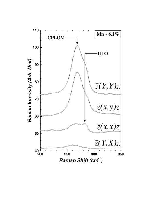
Typical Raman spectra of Ga1-xMnxAs with 6.1 Mn at room temperature in quasi-backscattering geometry with different polarization configurations are displayed in Fig. 1, where is the growth direction and , , , and . According to the Raman selection rule for a zinc-blende crystal, the LO phonon is allowed for and but forbidden for and whereas TO phonon is forbidden for all the scattering configurations employed in Fig. 1. porto The Raman feature near 269 is very strong in and whereas it is extremely weak in and where LO modes are forbidden. This reveals its “LO mode” nature despite its proximity to the GaAs TO frequency. The very weak Raman signal near in configuration is the disorder-induced TO phonon that should exist as a weak background Raman intensity for all the other scattering configurations employed in Fig. 1. Thus, the Raman feature at 269 is a CPLOM in Ga0.94Mn0.06As. We have not observed any Raman signature in the high frequency spectral range up to 1700 that can be attributed to . This indicates that the free carrier is a hole. Apart from the strong CPLOM in , there is an unmistakable shoulder on the high frequency side of the CPLOM. This is due to the ULO in the depletion layer near the surface. It is more distinctly observed in , where the LO mode is forbidden due to Raman selection rules. However, the electric field near the semiconductor surface causes a relaxation of Raman selection rules.
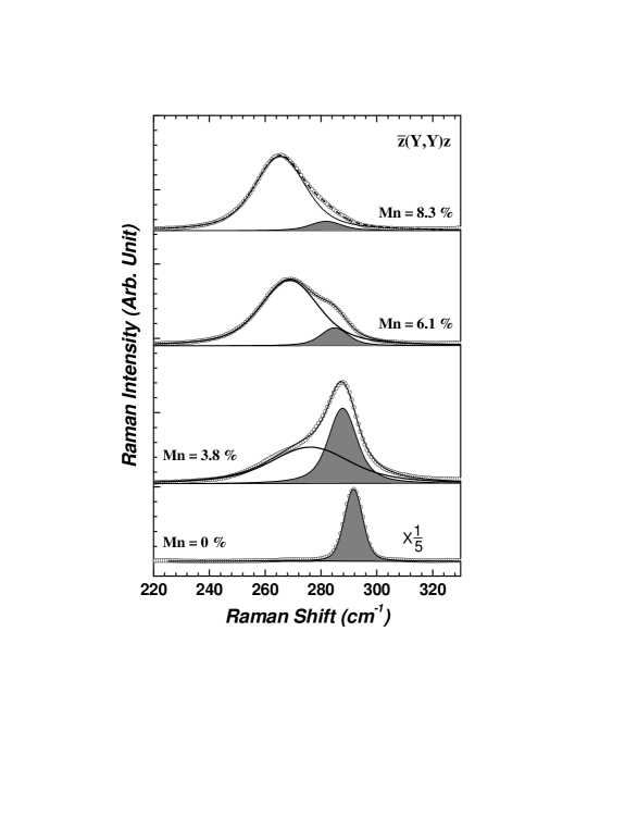
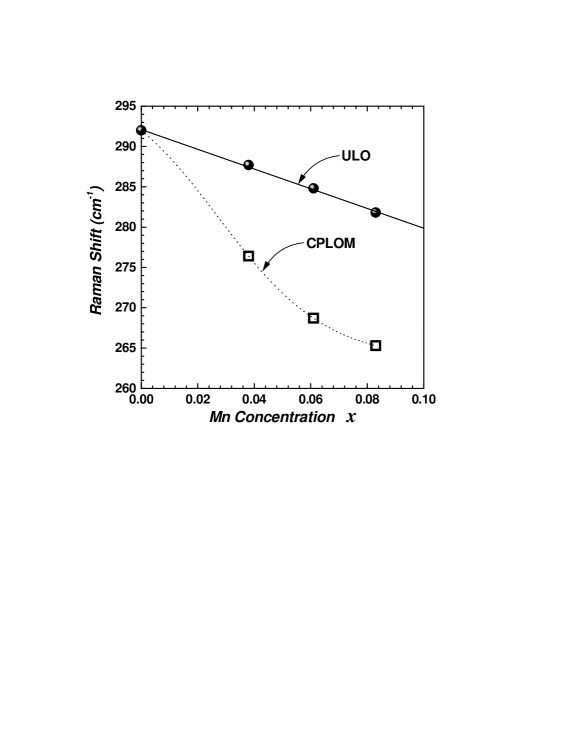
In the configuration, the superimposed Raman features can be decomposed into CPLOM and ULO parts by fitting the the experimental data using two Lorentzian oscillators as shown in Fig. 2, where Raman spectra of Ga1-xMnxAs for , and in scattering configuration are displayed. It should be noted that the Raman spectrum of the reference sample () consists of only one Lorentzian oscillator. The Raman intensity of the ULO (shaded area) rapidly decreases as the Mn concentration increases. The peak positions of the CPLOM and ULO determined from the curve fitting are listed in Table 1 and shown in Fig. 3. The ULO frequency linearly decreases with increasing Mn concentrations up to 8.3%. Since the lattice constant of Ga1-xMnxAs increases with increasing the compressive strain in the GaMnAs layer should induce a blue-shift of the ULO frequency. However, the alloying effect appears to be much stronger than the strain effect in Ga1-xMnxAs, leading to the observed ULO frequency red-shift with increasing .
| Mn concentration (%) | ULO () | CPLOM () | (Å) | () |
|---|---|---|---|---|
| 0 | 291.7 1.0 | |||
| 3.8 0.2 | 287.7 1.0 | 276.4 1.0 | 76 4 | |
| 6.1 0.2 | 284.8 1.0 | 268.7 1.0 | 16 1 | 2.8 |
| 8.3 0.2 | 281.8 1.0 | 265.3 1.0 | 10 0.5 | 7.1 |
Traditionally, lineshape analysis of Raman scattering for the CPLOM has been used to deduce carrier concentrations of -type GaAs irmer97 ; mlayah91 , assuming that the phonon frequencies of the TO and LO phonon do not change with doping. This is valid because conventional dopant concentrations are too small to change most of the physical parameters of GaAs used for the lineshape analysis. However, Mn concentrations in Ga1-xMnxAs samples for are high enough to change the frequency of the ULO as shown in Table 1, making it incorrect to use the GaAs parameters for the lineshape analysis of the CPLOM. Alternatively the -type carrier concentration can be determined by analyzing the relative intensities of ULO and CPLOM. irmer97 Assuming the Raman scattering efficiency from the ULO is similar to that in an undoped crystal, the integrated intensity of the ULO can be written as pinczuk79
| (1) |
where is the integrated intensity in an undoped crystal, is the absorption coefficient, and is the depletion layer thickness. Since the integrated Raman intensity is proportional to the scattering volume, is given by
| (2) |
where is the integrated intensity of the CPLOM and is the relative Raman scattering efficiencies of the ULO and CPLOM in a unit volume. Using Eqs. (1) and (2), can be estimated from the experimental Raman data
| (3) |
where is the ratio of the integrated intensity of the ULO to that of CPLOM in the Raman spectrum. The depletion layer thickness for can be calculated as a function of hole concentration at zero temperature (neglecting transition region)
| (4) |
where is the static dielectric constant and is the surface potential barrier. irmer97 Since the values of and for GaMnAs are not available we used those for GaAs, [Ref. blakemore82 ] and [Ref. borisova72 ]. By comparing for and for in Fig. 2 we have obtained and used this value for the analysis of all . Since the ULO Raman efficiency in principle could be dependent on there is a small uncertainty introduced by using a constant value of . But a close inspection showed that is almost constant for all four samples, making a good approximation. We also used for the excitation wavelength . aspnes83 By equating Eqs. (4) and (3), is given by
| (5) |
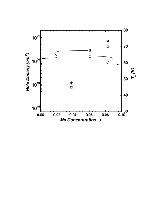
and thus calculated hole concentrations are listed in Table 1, with an uncertainty less than 10%. It is worth mentioning here that any possible uncertainty in and would affect only the scaling factor in Eq. 5. In order to check any possible finite temperature correction in our analysis, we have analyzed the Raman spectrum of the 6.1% sample measured at and obtained the same hole concentration within the error bar as shown in Table 1. The hole concentration monotonically increases up to for the 8.3% sample, showing a good correlation with (Fig. 4). This is different from the results of Matsukura et al. matsukura98 where the hole concentration, measured using Hall effect, and reached its maximum value and , respectively, for and then decreased with increasing Mn concentration for . The difference between the two results can be attributed to differences in detailed growth conditions. However, the fact that the hole concentration, determined by Raman scattering, and show a similar monotonic increase with increasing provides further confidence in our spectroscopically determined values of the hole density in Ga1-xMnxAs.
In conclusion, we have determined the room temperature carrier concentration in Ga1-xMnxAs for , and using Raman intensity analysis of the coupled plasmon-LO-phonon mode and the unscreened LO phonon. This study shows that – unlike standard Hall measurements – Raman scattering provides an unambiguous and reliable method of determining the hole density in Ga1-xMnxAs that can be profitably exploited for gaining a better understanding of the origins of ferromagnetism in ferromagnetic semiconductors.
Work at NREL was supported by the Office of Science (Material Science Division) of the Department of Energy under Contract No. DE-AC36-99GO10337 as well as the NREL DDRD program. Work at PSU was supported by DARPA and ONR under grants N00014-99-1-1093, N00014-99-1-0071 and N00014-99-1-0716. HMC was supported by grant No. 2000-2-30100-009-3 from the Basic Research Program of the Korea Science and Engineering Foundation.
References
- (1) S. A. Wolf, D. D. Awschalom, R. A. Buhrman, J. M. Daughton, S. von Molnar, M. L. Roukes, A. Y. Chtchelkanova, D. M. Treger, Science 294, 1488 (2001).
- (2) Semiconductor and Semimetals, edited by J. K. Furdyna and J. Kossut (Academic, New York, 1988), Vol. 25.
- (3) D. D. Awschalom and N. Samarth, J. Magn. Magn. Mater. 200, 130 (1999) and references therein.
- (4) H. Ohno, J. Magn. Magn. Mater. 200, 110 (1999) and references therein.
- (5) T. Dietl, H. Ohno, F. Matsukura, J. Cibert, D. Ferrand, Science 287, 1019 (2000).
- (6) H. Ohno, A. Shen, F. Matsukura, A. Oiwa, A. Endo, S. Katsumoto, and Y. Iye, Appl. Phys. Lett. 69, 363 (1996).
- (7) J. De Boeck, R. Oesterholt, A. Van Esch, H. Bender, C. Bruynseraede, C. Van Hoof, and G. Borghs, Appl. Phys. Lett. 68, 2744 (1996).
- (8) F. Matsukura, H. Ohno, A. Shen, and Y. Sugawara, Phys. Rev. B 57, R2037 (1998).
- (9) J. König, H. H. Lin, and A. H. MacDonald, Phys. Rev. Lett. 84, 5628 (2000).
- (10) H. Ohno and F. Matsukura, Solid State Comm. 117, 179 (2001).
- (11) A. Mooradian and G. B. Wright, Phys. Rev. Lett. 16, 999 (1966).
- (12) G. Irmer, M. Wenzel, and J. Monecke, Phys. Rev. B 56, 9524 (1997).
- (13) S. J. Potashnik, K. C. Ku, S. H. Chun, J. J. Berry, N. Samarth, and P. Schiffer, Appl. Phys. Lett. 79, 1495 (2001).
- (14) We have used the conventional Porto’s notation , where and are propagation directions of incoming and scattered photon, respectively, and and are directions of polarizer and analyzer for incoming and scattered photon, respectively.
- (15) A. Mlayah, R. Carles, G. Landa, E. Bedel, and A. Muñoz-Yagüe, J. Appl. Phys. 69, 4064 (1991).
- (16) A. Pinczuk, A. A. Ballman, R. E. Nahory, M. A. Pollack, and J. M. Worlock, J. Vac. Sci. Technol., 16, 1168 (1979).
- (17) J. S. Blakemore, Appl. Phys. 53, R123 (1982).
- (18) L. A. Borisova, A. F. Kravcenko, K. N. Kot, and E. M. Skok, Fiz. Tekh. Poluprovodn. 6, 799 (1972) [Sov. Phys. Semicond. 6, 693 (1972)].
- (19) D. E. Aspnes and A. A. Studna, Phys. Rev. B 27, 985 (1983).