Effects of accidental microconstriction on the quantized conductance in long wires
Abstract
-
† Department of Physics and Measurement Technology,
Linköping University, S-581 83 Linköping, Sweden
‡ Kirensky Institute of Physics, 660036, Krasnoyarsk, Russia
§Cavendish Laboratory, Madingley Road,
Cambridge CB3 00HE, United Kingdom
-
Abstract. We have investigated the conductance of long quantum wires formed in heterostructures. Using realistic fluctuation potentials from donor layers we have simulated numerically the conductance of four different kinds of wires. While ideal wires show perfect quantization, potential fluctuations from random donors may give rise to strong conductance oscillations and degradation of the quantization plateaux. Statistically there is always the possibility of having large fluctuations in a sample that may effectively act as a microconstriction. We therefore introduce microconstrictions in the wires by occasional clustering of donors. These microconstrictions are found to restore the quantized plateaux. A similar effect is found for accidental lithographic inaccuracies.
-
† Department of Physics and Measurement Technology,
Linköping University, S-581 83 Linköping, Sweden
‡ Kirensky Institute of Physics, 660036, Krasnoyarsk, Russia
§Cavendish Laboratory, Madingley Road,
Cambridge CB3 00HE, United Kingdom
-
Abstract. We have investigated the conductance of long quantum wires formed in heterostructures. Using realistic fluctuation potentials from donor layers we have simulated numerically the conductance of four different kinds of wires. While ideal wires show perfect quantization, potential fluctuations from random donors may give rise to strong conductance oscillations and degradation of the quantization plateaux. Statistically there is always the possibility of having large fluctuations in a sample that may effectively act as a microconstriction. We therefore introduce microconstrictions in the wires by occasional clustering of donors. These microconstrictions are found to restore the quantized plateaux. A similar effect is found for accidental lithographic inaccuracies.
Introduction
Long quantum wires are important objects from the view of both technology and fundamental physics (see for example [1, 2, 3] and references cited). Theory predicts that conductance through long clean wires is perfectly quantized with much sharper features than usual QPCs. However, the practical manufacturing of perfect, high quality wires is a delicate task. Thus many factors may influence the conductance in real devices and may cause deviations from theoretical predictions. Potential fluctuations from donors, small tolerance to possible inaccuracies in the lithography of gates are some of these factors. There could be two reasons for good quantization of the measured conductance in a long wire: either a superior quality of the wire or effects not connected with quantum properties of the entire wire, like local potential fluctuations from donors or defects. For example, in some samples we have observed quite well defined plateaux that degrade on thermal cycling. Does it mean that the potential landscape is changed in this process in such way that an occasional microconstriction is removed?
In this work we discuss the conductance of long wires in heterostructures. We consider some accidental effects that could produce well shaped quantized plateaux. In particular, we study how donors and lithographical deffects can produce QPC-like substructures and change the shape of the conductance plateaux characteristics.
1 Theoretical model and calculation
Long quantum wires are often fabricated in modulation-doped heterostructure with a patterned metallic top gate, see Fig. 1a.
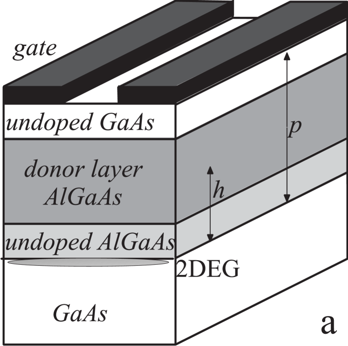
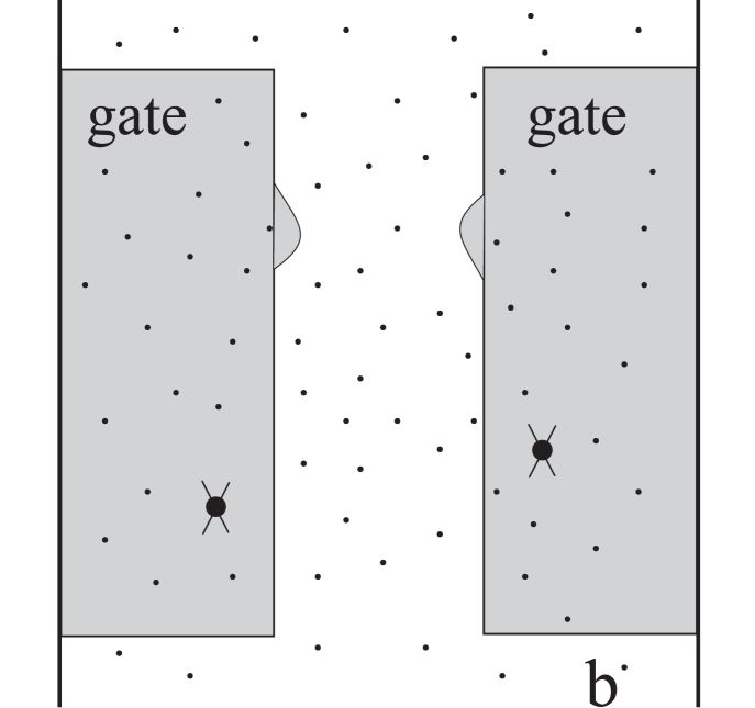
Figure 1: a) Schematic representation of a device simulating a long quantum wire; b) Donors in the doped (dots), points of concentration of donors (crosses), irregularities of the shape the gates. Corresponding confinement potentials are smoothed. A negative voltage applied to the gate relative to the substrate depletes the two-dimensional electron gas (2DEG) under the gated regions and leaves a conducting wire in the split gate region. The actual size of the wire can be varied lithographically by changing the geometry of the gate as well as by varying the applied voltage. The confinement potential formed by the gate is determined by the well known expression [4] :
(1) where is the potential on the gate and the distance between the gate and the 2DEG. To investigate possible effects in real devices we introduce the potential from random donors and mirror charges as described in [5] :
(2) where the summation is over all donor positions in the plane on distance from the 2DEG. Mirror charges are generated by the surface at distance from the 2DEG in Fig. 1a.
To find the electronic configuration and related properties of the system we have solved the Schrödinger equation for electrons of a mass mapped on a square lattice:
(3) The zero-temperature conductance was calculated as according to the Büttiker formula; is the transmission matrix. We use this one electron approach because we believe that brings out the essential physics in the problem.
In the following we consider four variants of long wires:
a) a wire with uniform potential (ideal wire);
b) a wire with a fluctuating potential to mimic a real device.
We also consider two additional cases associated with possible problems of manufacturing long wires. In both cases we assume that there are background potential fluctuations from random donors as in b). Thus we also have
c) a wire with clusters of donors. We simply let more than one donor sit at the same point as shown in Fig. 1b. The clusters represent statistical variations in donor concentration and/or impurities or other imperfections from the growth of the heterostructure;
d) the top gate has deviations from the regular shape as shown in Fig. 1b. As a result an additional QPC microconstriction in the wire is formed.
We have studied wires formed by split gates as in Fig. 1. The lithographic length is and the gap between gates is wide. Typical size of the numerical grid is 70x1000.
2 Results and discussion
The calculated conductance as a function of applied gate voltage is show in Fig. 2. As indicated, the conductance for an ideal wire (dotted line) shows well-shaped sharp stairs. The dashed line on the same figure represents transport through the same long wire with potential fluctuations from random donors.
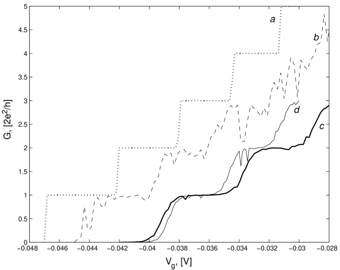
Figure 2: Calculated zero-temperature conductance for long wires. a) ideal wire; b) wire with fluctuated potential; c) microconstriction substructure formed by donor potential; d) microconstriction substructure from irregular gates. In this case the quantization is degraded because of backscattering and interference effects. Depending on the particular realization of random positions of donors the conductance oscillations differ from sample to sample. The situation changes dramatically when we add two donors having larger charge, that represent local concentrations/statistical clusters of donors or other imperfections. This case is shown by the bold solid line. Donors situated on the different sides of the channel may form a QPC-like structure which plays a dominant role in the transport process through the channel. The case when a QPC-like structure is formed by lithographic irregularities in the gates looks similar. However, the main difference between the two cases is the width of the plateaux which is a result of the different mechanisms behind the formation the QPC-like structures. In the case of gate irregularities the potential is more responsive to the applied voltage, it acts like a normal QPC (Fig. 2d.). In contrast, when the narrowing is due to donor concentrations/clusters etc., variation of voltage does not change the structure of local QPC-potential. Instead the voltage only shifts the entire potential landscape. In this case the plateaux are wider indicating less dependence on gate voltage (Fig. 2c).
In conclusion, the microconstrictions in long quantum wires may play a dominant role in transport processes. Good quantization may be observed not only in the case of well manufactured devices but also for imperfect wires with microconstricitions. Experimentally it may be a problem to recognize what kind of situation we have at hand. One possible way is to compare wires with the same geometry. Plateaux for QPC substructures are shifted with gate voltage and have different shapes which may be analyzed by means of a local saddle-point model.
Acknowledgments
This work has been supported by the the Royal Swedish Academy of Sciences (AAS) and the Engineering and Physical Sciences Research Council, UK (ACG). KJT acknowledges support from Royal Society Research Fellowship, UK.
References
- [1] S. Tarucha, T. Honda and T. Saku, Solid State Commun. 94, 413 (1995)
- [2] C.-T. Liang, M. Pepper, M.Y. Simmons, C.G. Smith and D.A. Ritchie, Phys. Rev. B 61, 9952 (2000)
- [3] D.J. Reilly, G.R. Facer, A.S. Dzurak, B.E. Kane, R.G. Clark, P.J. Stiles, R.G. Clark, A.R. Hamilton, J.L. O’Brien, N.E. Lumpkin, L.N. Pfeiffer and K.W. West, Phys. Rev. B 63, R121311 (2001)
- [4] J.H. Davies, Semicond. Sci. Technol. 3, 995 (1988);
- [5] J.H. Davies and J.A. Nixon, Phys. Rev. B 39, 3423 (1989).