Current address: ]Cielo Communications, Inc., 325 Interlocken Parkway, Broomfield, CO 80021.
Superconducting Single-Electron Transistor in a Locally Tunable Electromagnetic Environment: Dissipation and Charge Fluctuations
Abstract
We have developed a novel system consisting of a superconducting single-electron transistor (S-SET) coupled to a two-dimensional electron gas (2DEG), for which the dissipation can be tuned in the immediate vicinity of the S-SET. Within linear response, the S-SET conductance varies nonmonotonically with increasing 2DEG impedance. We find good agreement between our experimental results and a model incorporating electromagnetic fluctuations in both the S-SET leads and the 2DEG, as well as low-frequency switching of the S-SET offset charge.
pacs:
74.50.+r,73.23.Hk,74.40.+kElectrical transport in nanoscale devices is strongly affected by the electromagnetic properties of their environment. This is particularly true for superconducting systems, and has been a topic of considerable interest lately: dissipation can drive a superconductor-insulator quantum phase transition Rimberg et al. (1997); Mason and Kapitulnik (1999); Penttilä et al. (1999), and is also expected to affect the coherence time of qubits such as the charge-based single Cooper pair box Bouchiat et al. (1998); Nakamura et al. (1999); Makhlin et al. (1999). Maintaining quantum coherence in such devices long enough to allow many operations is prerequisite for their use in quantum computation. In this regard, the closely related superconducting single electron transistor (S-SET) is an excellent system for attaining a better understanding of the effects of the electromagnetic environment on quantum coherence.
This approach was followed by the Berkeley group Kycia et al. (2001), who fabricated an S-SET above a two-dimensional electron gas (2DEG) in a GaAs/AlxGa1-xAs heterostructure. Using a back gate to vary the 2DEG sheet resistance they measured changes in the S-SET conductance as the dissipation was varied. Building on earlier theoretical work Devoret et al. (1990); Ingold and Nazarov (1992); Grabert et al. (1998); Dittrich et al. (1998); Ingold and Grabert (1999), Wilhelm, et al. predicted Wilhelm et al. (2001) that within linear response would scale with the ground plane conductance and temperature T as and that the S-SET current at fixed bias voltage would vary nonmonotonically with , while switching from the non-linear to linear regime. These predictions were made within two models: in one the environment was treated as a ground plane, while in the other it was treated as an infinite transmission line provided by the SET leads. While the Berkeley group did observe power law behavior, their measured exponents were not in quantitative agreement with theory. Furthermore, the measured depended on and on , calling the scaling form into question.
In this Letter, we report measurements on samples similar to those studied by the Berkeley group; in our samples, however, we can modify in the immediate vicinity of the S-SET while leaving the 2DEG beneath the leads largely untouched. In contrast to the predictions of Wilhelm, et al. we observe a nonmonotonic dependence of on entirely within the linear regime. We propose a model for the environmental impedance of S-SET/2DEG systems that includes electromagnetic fluctuations in both the 2DEG and leads, while treating the latter as finite transmission lines. We also allow for relatively low-frequency switching of the charge state of the SET islandEiles and Martinis (1994), which can affect the measured current. Within this model, we find good agreement between our calculated and measured results.
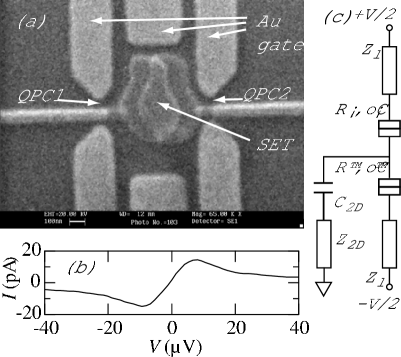
An electron micrograph of a typical sample is shown in Fig. 1(a). We begin with an GaAs/AlxGa1-xAs heterostructure grown on a GaAs substrate using molecular beam epitaxy, consisting of the following layers: of GaAs, of Al0.3Ga0.7As and of GaAs. The Al0.3Ga0.7As is delta-doped with Si from the lower GaAs/Al0.3Ga0.7As interface, at which forms a two-dimensional electron gas (2DEG) with and sheet density . On the sample surface we use electron-beam lithography and shadow evaporation to fabricate an S-SET surrounded by six Au gates Lu et al. (2000). When no gate voltage is applied and the 2DEG is unconfined, the measured - characteristics are linear over several microvolts, as shown in Fig. 1(b). We can also apply a single gate voltage to any combination of Au gates, excluding the 2DEG beneath them. We focus on two geometries: the “pool,” in which all six gates are energized, and the “stripe” in which only the four exterior gates are. In both cases, electrons immediately beneath the SET are coupled to ground by quantum point contacts (QPCs) with conductances (assumed equal) as low as 3 conductance quanta . In the stripe geometry, the electrons can also move vertically through a resistance to a large 2DEG reservoir that is coupled to ground through a capacitance . As illustrated in Fig. 1(c), electromagnetic fluctuations in the environment can couple to the tunneling electrons in two ways: through the leads, which act as transmission lines with impedance for the relevant frequency range Kycia et al. (2001); Wilhelm et al. (2001), and through the capacitance to the 2DEG with impedance , which is related to and (for the stripe) . The model has been studied previously Odintsov et al. (1991); Ingold et al. (1991) without considering particular forms for and .
Measurements were performed on two separate samples (S1 and S2) in a dilution refrigerator in a four-probe voltage biased configuration; the estimated electron temperature was . High frequency noise was excluded using standard techniques. A small capacitance (not shown in Fig. 1(c)) couples the six Au gates to the S-SET. The other sample parameters such as the junction resistances and capacitances , the coupling capacitance and superconducting gap are given elsewhere Lu et al. (2002). The charging energy for sample S1 (S2) is while the Josephson energy averaged for the two junctions is . Here is the superconducting resistance quantum and . We use standard lock-in techniques and voltage biases of 3 and respectively to measure and the conductance across the series combination of the QPCs versus in the pool and stripe geometries. The results for S2 are shown in Fig. 2.
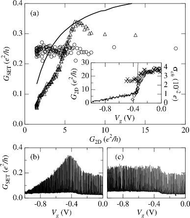
From Fig. 2(b), we see that for the pool rises by nearly a factor of 2 as becomes more negative, before dropping rapidly. Although vs. is nearly identical in both cases, for the stripe rises only by 50% and does not decrease, even for the most negative . In both plots, -periodic Coulomb blockade oscillations are seen as the S-SET offset charge varies. We fit a smoothly varying function to the measured versus (inset, Fig. 2(a)) which we use to plot the maxima of versus in Fig. 2(a). The knee in at corresponds to the appearance of quantized plateaux in the individual QPC conductances.
To understand these results and the - curve in Fig. 1 (b), we begin with the rate of sequential Cooper pair tunneling Averin et al. (1990) through junction , valid for
| (1) |
where is the free energy difference for changing the number of Cooper pairs by 1, , and . Here P(E) is the probability of exchanging energy with the environment and can be expressed in terms of a correlation function via where is the total impedance seen by tunneling electrons.
The general result for within the model of Fig. 1(c) is quite complex Ingold et al. (1991). In our case, however, () dominates at low (high) frequencies and to an excellent approximation
| (2) |
where for junction 1(2) , , and we treat as a resistance. For we begin with the impedance of a finite line where and are the resistance and capacitance per unit length and is the total line length. We are interested in the long-time limit of which is dominated by the low-frequency part of . In that limit, , which we use for in Eq. 2.
A detailed analysis of will be given elsewhere. Here we note that both parts of in Eq. 2 have the same form. For , the corner frequency satisfies and we may use the kernel of Ref. Wilhelm et al., 2001, while for we find that usually satisfies and requires different treatment. Since is linear in , we may calculate and separately for and and find the total as a convolution. For , then, we have where and is the beta function Wilhelm et al. (2001). For , we find that
| (3) |
is valid for , where and . From this we calculate
| (4) |
where , , and is the incomplete gamma function.
To proceed we need an accurate model of . For the - curve to be linear at , must be nonnegligible at frequencies of order . Since then , must dominate for small . We therefore consider the structure of our leads, which vary in width from to . The section has length , contributes only to , and is not considered further. For the remaining sections with 0.4, 1.0, 10 and , and 9, 57, 253 and we use and where is the 2DEG depth and the dielectric constant of GaAs to calculate 29, 16, 1.9 and and 1.1, 2.5, 23 and . These four sections form a cascaded line which determines . The total calculated from Eq. 2 is shown for different values of for the pool geometry in Fig. 3. The cascaded form for is quite complex. For our calculations we take where the are the impedances of the individual sections, a very good approximation to the more exact result, as shown. Note that this model predicts a significant at dominated by () for small (large) . For the stripe, approaches at zero frequency and the much lower stripe resistance at frequencies above where is its capacitance to ground. At high frequencies, then, in the stripe is always dominated by , even for large negative . We have also shown the impedance for alone, and for an infinite line with and chosen to give the correct if the line were finite. The latter two models give a small for small at the relevant frequencies, and cannot explain the linear region in our - characteristics.

Using and above, we numerically convolve the for junction and section to find . We then calculate for different and set up a master equation using the rates in Eq. 1 to calculate the S-SET current and conductance . The results for in the pool geometry are shown as the solid line in Fig. 2(a); we scale to match the maximum measured value at but use no other variable parameters. agrees reasonably well with for although it rises less steeply with . In this regime is broad and inelastic transitions suppress the coherent supercurrent. For , gradually saturates at . For , (i. e., only elastic transitions are likely) and dominates the - characteristic. No nonmonotonic behavior occurs in , in agreement with Wilhelm et al. The drop in for must arise from other physics.

We can model the drop by assuming that the measured and are actually averaged over charge states close to , due to charge motion in the substrate Eiles and Martinis (1994). We expect charge averaging to be most pronounced when the 2DEG is unconfined, and least for small . Assuming a Gaussian distribution of charge states with mean and variance , we calculate the average . We do not know the absolute size of , so we assume for the pool that for . For we find the values of which give for the pool and stripe and plot the results in the inset to Fig. 2(a). In both cases is just below near and drops near . For the stripe, saturates at just above , about half the drop for the pool. The model seems reasonable given the small required to explain the discrepancies with the environmental theory.
We gain further confidence in the model by comparing measured and calculated - characteristics for the pool, as shown in Fig. 4 for S1. For increasing confinement first rises at all voltages, with little or no broadening of the linear region ( and and ). This corresponds to a reduction in with little change in ; inelastic transitions in the leads dominate the energy exchange. Eventually, and is large enough to affect , causing to decrease (especially at low bias) and the linear region to broaden. The level of agreement between the shape and evolution of the measured and calculated curves is surprisingly good, given the uncertainties involved. While the calculated current is much larger than is measured, such discrepancies are common in small tunnel junction systems Eiles and Martinis (1994).
In conclusion, we have measured the effects of dissipation on transport in an S-SET for which the environment can be varied locally. We find good agreement with a model in which fluctuations in the leads and low-frequency switching between charge states dominate for low confinement (large ), while for strong confinement (small ) fluctuations coupled via the capacitance dominate. The model accounts well for the evolution of and the - curves as is varied. We believe a convolved is likely required to interpret the results of the Berkeley group, which may explain the discrepancies between their results and the scaling theory of Wilhelm, et al.
This research was supported at Rice by the NSF under Grant No. DMR-9974365 and by the Robert A. Welch foundation, and at UCSB by the QUEST NSF Science and Technology Center. One of us (A. J. R.) acknowledges support from the Alfred P. Sloan Foundation. We thank A. C. Gossard for providing the 2DEG material.
References
- Rimberg et al. (1997) A. J. Rimberg, T. R. Ho, Ç. Kurdak, J. Clarke, K. L. Campman, and A. C. Gossard, Phys. Rev. Lett. 78, 2632 (1997).
- Mason and Kapitulnik (1999) N. Mason and A. Kapitulnik, Phys. Rev. Lett. 82, 5341 (1999).
- Penttilä et al. (1999) J. S. Penttilä, Ü. Parts, P. J. Hakonen, M. A. Paalanen, and E. B. Sonin, Phys. Rev. Lett. 82, 1004 (1999).
- Nakamura et al. (1999) Y. Nakamura, Yu. A. Pashkin, and J. S. Tsai, Nature 398, 786 (1999).
- Bouchiat et al. (1998) V. Bouchiat, D. Vion, P. Joyez, D. Esteve, and M. H. Devoret, Phys. Scripta T76, 165 (1998).
- Makhlin et al. (1999) Yu. Makhlin, G. Schön, and A. Shnirman, Nature 398, 305 (1999).
- Kycia et al. (2001) J. B. Kycia, J. Chen, R. Therrien, Ç. Kurdak, K. L. Campman, A. C. Gossard, and J. Clarke, Phys. Rev. Lett. 87, 017002 (2001).
- Devoret et al. (1990) M. H. Devoret, D. Esteve, H. Grabert, G.-L. Ingold, H. Pothier, and C. Urbina, Phys. Rev. Lett. 64, 1824 (1990).
- Ingold and Nazarov (1992) G.-L. Ingold and Yu. V. Nazarov, in Single Charge Tunneling, edited by H. Grabert and M. H. Devoret (Plenum, New York, 1992), pp. 21–107.
- Grabert et al. (1998) H. Grabert, G.-L. Ingold, and B. Paul, Europhys. Lett. 44, 360 (1998).
- Dittrich et al. (1998) T. Dittrich, P. Hänggi, G.-L. Ingold, B. Kramer, G. Schön, and W. Zwerger, Quantum Transport and Dissipation (Wiley-VCH, Weinheim, Germany, 1998).
- Ingold and Grabert (1999) G.-L. Ingold and H. Grabert, Phys. Rev. Lett. 83, 3721 (1999).
- Wilhelm et al. (2001) F. K. Wilhelm, G. Schön, and G. T. Zimányi, Phys. Rev. Lett. 87, 136802 (2001).
- Eiles and Martinis (1994) T. M. Eiles and J. M. Martinis, Phys. Rev. B 50, 627 (1994).
- Lu et al. (2000) W. Lu, A. J. Rimberg, K. D. Maranowski, and A. C. Gossard, Appl. Phys. Lett. 77, 2746 (2000).
- Odintsov et al. (1991) A. A. Odintsov, G. Falci, and G. Schön, Phys. Rev. B 44, 13 089 (1991).
- Ingold et al. (1991) G.-L. Ingold, P. Wyrowski, and H. Grabert, Z. Phys. B 85, 443 (1991).
- Lu et al. (2002) W. Lu, K. D. Maranowski, and A. J. Rimberg, Phys. Rev. B 65, 060501 (2002).
- Averin et al. (1990) D. V. Averin, Yu. V. Nazarov, and A. A. Odintsov, Physica B 165&166, 945 (1990).